EP0484167A1 - Laserdiodenmodul mit Glasfaserausgang - Google Patents
Laserdiodenmodul mit Glasfaserausgang Download PDFInfo
- Publication number
- EP0484167A1 EP0484167A1 EP91310099A EP91310099A EP0484167A1 EP 0484167 A1 EP0484167 A1 EP 0484167A1 EP 91310099 A EP91310099 A EP 91310099A EP 91310099 A EP91310099 A EP 91310099A EP 0484167 A1 EP0484167 A1 EP 0484167A1
- Authority
- EP
- European Patent Office
- Prior art keywords
- laser diode
- ferrule
- package
- bellows
- fixed
- Prior art date
- Legal status (The legal status is an assumption and is not a legal conclusion. Google has not performed a legal analysis and makes no representation as to the accuracy of the status listed.)
- Granted
Links
- 239000000835 fiber Substances 0.000 title description 2
- 239000013307 optical fiber Substances 0.000 claims abstract description 14
- 238000007789 sealing Methods 0.000 claims description 3
- 229910052802 copper Inorganic materials 0.000 claims description 2
- 229910052737 gold Inorganic materials 0.000 claims description 2
- 229910052759 nickel Inorganic materials 0.000 claims description 2
- 230000003287 optical effect Effects 0.000 abstract description 15
- 238000006073 displacement reaction Methods 0.000 abstract description 4
- 230000007613 environmental effect Effects 0.000 description 7
- 229910000679 solder Inorganic materials 0.000 description 4
- 238000003466 welding Methods 0.000 description 3
- 230000008602 contraction Effects 0.000 description 2
- 238000005476 soldering Methods 0.000 description 2
- 230000008878 coupling Effects 0.000 description 1
- 238000010168 coupling process Methods 0.000 description 1
- 238000005859 coupling reaction Methods 0.000 description 1
- 239000002184 metal Substances 0.000 description 1
- 229910052751 metal Inorganic materials 0.000 description 1
- 230000002093 peripheral effect Effects 0.000 description 1
- 230000000717 retained effect Effects 0.000 description 1
Images
Classifications
-
- G—PHYSICS
- G02—OPTICS
- G02B—OPTICAL ELEMENTS, SYSTEMS OR APPARATUS
- G02B6/00—Light guides; Structural details of arrangements comprising light guides and other optical elements, e.g. couplings
- G02B6/24—Coupling light guides
- G02B6/42—Coupling light guides with opto-electronic elements
- G02B6/4201—Packages, e.g. shape, construction, internal or external details
- G02B6/4204—Packages, e.g. shape, construction, internal or external details the coupling comprising intermediate optical elements, e.g. lenses, holograms
-
- G—PHYSICS
- G02—OPTICS
- G02B—OPTICAL ELEMENTS, SYSTEMS OR APPARATUS
- G02B6/00—Light guides; Structural details of arrangements comprising light guides and other optical elements, e.g. couplings
- G02B6/24—Coupling light guides
- G02B6/42—Coupling light guides with opto-electronic elements
- G02B6/4201—Packages, e.g. shape, construction, internal or external details
- G02B6/4248—Feed-through connections for the hermetical passage of fibres through a package wall
Definitions
- the present invention relates to a laser diode module, and more specifically to a laser diode module in which the optical axes of a laser diode and an optical fiber pig-tail are each relatively adjusted.
- a laser diode (hereinafter referred to as "LD") module used in optical fiber communication is often marketed in the form of a module provided with an optical fiber pig-tail guiding light output power and is used under an extensive environmental condition ranging from the low to high temperatures.
- LD laser diode
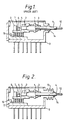
- Fig. 1 illustrates a longitudinal cross section of a conventional LD module.
- a laser diode (LD) chip 5 is adjusted in optical axis relative to a ferrule 4 via a lens 2 and the ferrule 4 is fixed to a base 1 via a slide ring 3 by YAG laser welding.
- An optical fiber 12 is protected at a proximate end by a ferrule 4 which is a metal pipe hermetically surrounding the optical fiber.
- the base 1 is fixed to a pakage 9 by soldering, with a Peltier element 11 interleaved therebetween.
- the ferrule 4 is fixed to the end wall of the package 9 by a solder lib in a manner to be hermetically sealed.
- the LD module Since the LD module is usually used under an extensive environmental condition ranging from -20 °C to + 70°C , within this range, it is required to retain a stable performance.
- the conventional package arranged as above expands about 60 ⁇ m in the axial direction of the fiber within the atmosphere of + 70°C as compared with a case under the normal temperature (25 °C). This displacement causes mechanical movement of the ferrule 4 fixed by a solder 14. When the ferrule 4 receives such a force, the base 1 would be deformed by being pushed by the ferrule, causing a deviation of the optical axes for the LD chip 5 and the ferrule 4. As a result, the optical output power launched into the optical fiber 12 within the ferrule 4 fluctuates 1dB or more.
- an object of the present invention is to eliminate such drawback discussed above and provide a laser diode module which allows a stable optical output power to be achieved even for the fluctuating environmental temperature.
- a laser diode module comprising a package having first and second ends, a laser diode chip accommodated therein and a ferrule provided at the end of an optical fiber fixed to the laser diode chip at a predetermined optical position, the ferrule being supported near the first end of the package at its one end and, at the other end, extending through an aperture provided at the first end of the package, a bellows through which center hole the ferrule extends, and fixed to the package at its one end and fixed to the ferrule at the other end.
- the LD module has a base fixed to the package, and the ferrule is fixed to this base at its one end and is coupled to the package at the other end via the bellows.
- the ferrule may be divided into two portions so that the first portion is fixed to the base and the second portion is coupled to the package via the bellows.
- the package and the ferrule are coupled via the bellows, even under the environmental condition ranging from the low to high temperatures, a stable optical output can be coupled without the optical axes of the laser diode and the optical fiber pig-tail being misaligned.
- Fig. 2 illustrates a longitudinal cross section of a laser diode module according to a preferred embodiment of the present invention.
- a base 1 supports a lens 2 at its one end and one end of a ferrule 4 at the other end via a slide ring 3 fixed to the base 1 by means of an YAG laser welding.
- the base 1 is provided with an extension for supporting a laser diode chip 5, a heat sink 6, a chip carrier 7 for supporting these and a photodiode 8.
- the LD chip 5 is adjusted in optical axis relative to the ferrule 4 via the lens 2.
- the extension of the base 1 is opposed to an L-shaped member 10 of the package 9 at a predetermined interval, and a Peltier element 11 is disposed therebetween.
- the Peltier element 11 is fixed to the base 1 and the package 9 by means of soldering.
- the ferrule 4 at the tip end of the optical fiber pig-tail 12 extends outwardly through the aperture of the package 9.
- One end of the bellows 13 is fixed to the package about its aperture, extending coaxially with the ferrule 4, and its tip end is hermetically sealed to the outer peripheral surface of the ferrule 4 via a solder layer 14.
- the bellows 13 is, for example, an electroplated bellows formed of a multilayer film of Au, Ni and Cu and, in this embodiment, it has three crests and its spring constant assumes 0.1 kg/mm.
- the package 9 is deformed about 60 ⁇ m in the axial direction of the ferrule 4 due to thermal expansion/contraction. This deformation in turn causes a relative displacement corresponding thereto between the bellows 13 fixed to one end of the package and the ferrule supported to the other end of the package. This displacement is absorbed by expansion and contraction of the bellows 13. If the spring constant of the bellows is on the order of 0.1 kg/mm or less, then a mechanical stress is hardly applied to the ferrule 4 and the deformation of the package 9 is absorbed by the bellows 13. In consequence, the optical axes of the LD chip and the ferrule cannot misalign.
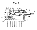
- Fig. 3 illustrates a longitudinal cross section of a second embodiment of the present invention.
- This LD module differs from that of Fig. 2 in that the ferrule 4 is divided into a first and second ferrules 41 and 42, which are both coupled by a bellows 13a.
- the second ferrule 42 constitutes a hermetic sealing portion of the package.
- the bellows 13a may be an electroplated bellows as in foregoing but, in this embodiment, it is a single Ni layer having two crests and its spring constant assumes 0.1 kg/mm.
- the first ferrule 41 is adjusted in optical axis relative to the LD chip 5, and is fixed to the base 1 via the slide ring 3 by YAG laser welding, while the second ferrule 42 is fixed to the package 9 by the solder layer 14, as in the conventional LD module of Fig. 1.
- the deformation wihtin the range of -20°C and + 70°C is absorbed by the bellows 13a which spring constant is small and, as in the first embodiment, a stable coupling can be retained against the fluctuating temperature.
Landscapes
- Physics & Mathematics (AREA)
- General Physics & Mathematics (AREA)
- Optics & Photonics (AREA)
- Optical Couplings Of Light Guides (AREA)
- Semiconductor Lasers (AREA)
Applications Claiming Priority (2)
| Application Number | Priority Date | Filing Date | Title |
|---|---|---|---|
| JP296096/90 | 1990-10-31 | ||
| JP02296096A JP3110039B2 (ja) | 1990-10-31 | 1990-10-31 | 半導体レーザモジュール |
Publications (2)
| Publication Number | Publication Date |
|---|---|
| EP0484167A1 true EP0484167A1 (de) | 1992-05-06 |
| EP0484167B1 EP0484167B1 (de) | 1995-05-17 |
Family
ID=17829078
Family Applications (1)
| Application Number | Title | Priority Date | Filing Date |
|---|---|---|---|
| EP91310099A Expired - Lifetime EP0484167B1 (de) | 1990-10-31 | 1991-10-31 | Laserdiodenmodul mit Glasfaserausgang |
Country Status (4)
| Country | Link |
|---|---|
| US (1) | US5247530A (de) |
| EP (1) | EP0484167B1 (de) |
| JP (1) | JP3110039B2 (de) |
| DE (1) | DE69109806T2 (de) |
Cited By (5)
| Publication number | Priority date | Publication date | Assignee | Title |
|---|---|---|---|---|
| WO1996024873A3 (en) * | 1995-02-10 | 1996-10-17 | Philips Electronics Nv | Optoelectronic device with a coupling between a semiconductor diode laser modulator or amplifier and two optical glass fibres |
| FR2769100A1 (fr) * | 1997-09-30 | 1999-04-02 | Kyocera Corp | Boitier pour dispositif photosemi-conducteur |
| EP1160599A1 (de) * | 2000-05-31 | 2001-12-05 | The Furukawa Electric Co., Ltd. | Halbleiterlaserdiodenmodul |
| WO2002093223A1 (en) * | 2001-05-16 | 2002-11-21 | Motorola Broadband Nürnberg GmbH | Device for holding an optical fiber |
| GB2390911A (en) * | 2002-06-14 | 2004-01-21 | Furukawa Electric Co Ltd | Optic fibre semiconductor module package |
Families Citing this family (22)
| Publication number | Priority date | Publication date | Assignee | Title |
|---|---|---|---|---|
| JPH04107862U (ja) * | 1991-02-28 | 1992-09-17 | 古河電気工業株式会社 | 半導体レーザモジユール |
| JPH05267775A (ja) * | 1992-03-19 | 1993-10-15 | Nec Corp | 半導体レーザ装置 |
| JPH06232504A (ja) * | 1993-01-29 | 1994-08-19 | Canon Inc | レーザ走査装置 |
| BE1006983A3 (nl) * | 1993-04-06 | 1995-02-07 | Koninkl Philips Electronics Nv | Opto-electronische inrichting met een koppeling tussen een opto-electronische component, in het bijzonder een halfgeleiderdiodelaser, en een optische glasvezel en werkwijze ter vervaardiging van een dergelijke inrichting. |
| JP2616671B2 (ja) * | 1993-09-25 | 1997-06-04 | 日本電気株式会社 | 光学モジュール装置 |
| US5717712A (en) * | 1995-09-12 | 1998-02-10 | Lucent Technologies Inc. | Laser communication system with temperature controlled |
| US5821530A (en) * | 1996-01-16 | 1998-10-13 | Wireless Control Systems, Inc | Coadunate emitter/detector for use with fiber optic devices |
| JP3076246B2 (ja) * | 1996-08-13 | 2000-08-14 | 日本電気株式会社 | ペルチェクーラ内蔵半導体レーザモジュール |
| KR100249518B1 (ko) | 1997-11-21 | 2000-03-15 | 이계철 | 열변형을 최소화하기 위한 완충 장치를 갖는 광스위치 모듈 |
| JP3345853B2 (ja) * | 1998-11-13 | 2002-11-18 | 古河電気工業株式会社 | レーザダイオードモジュールおよびその作製方法 |
| US6292615B1 (en) | 1999-03-09 | 2001-09-18 | Uniphase Telecommunications Products, Inc. | Optical fiber feedthrough |
| US6213651B1 (en) | 1999-05-26 | 2001-04-10 | E20 Communications, Inc. | Method and apparatus for vertical board construction of fiber optic transmitters, receivers and transceivers |
| US6901221B1 (en) | 1999-05-27 | 2005-05-31 | Jds Uniphase Corporation | Method and apparatus for improved optical elements for vertical PCB fiber optic modules |
| US6243508B1 (en) | 1999-06-01 | 2001-06-05 | Picolight Incorporated | Electro-opto-mechanical assembly for coupling a light source or receiver to an optical waveguide |
| JP4413417B2 (ja) * | 2000-12-18 | 2010-02-10 | 古河電気工業株式会社 | レーザダイオードモジュール |
| US6912237B2 (en) * | 2001-02-06 | 2005-06-28 | The Furukawa Electric Co., Ltd. | Semiconductor laser module and semiconductor laser device having light feedback function |
| JP2002343982A (ja) * | 2001-05-16 | 2002-11-29 | Mitsubishi Electric Corp | 光モジュール、光送信器及び光受信器 |
| US6538901B1 (en) * | 2002-03-05 | 2003-03-25 | Chen-Hung Hung | Optical transceiver module |
| US20050002613A1 (en) * | 2002-11-25 | 2005-01-06 | Michael Rehberger | LED device |
| DE10258745A1 (de) * | 2002-12-13 | 2004-07-08 | Hentze-Lissotschenko Patentverwaltungs Gmbh & Co.Kg | Halbleiterlaservorrichtung, Halbleiterlaserbaustein für eine derartige Halbleiterlaservorrichtung sowie ein Verfahren zur Herstellung einer derartigen Halbleiterlaservorrichtung |
| GB2477740B (en) * | 2010-02-10 | 2014-06-25 | Oclaro Technology Ltd | Reduced length optoelectronic devices |
| RU2584724C2 (ru) * | 2014-10-10 | 2016-05-20 | Открытое акционерное общество "Ракетно-космический центр "Прогресс" (ОАО "РКЦ "Прогресс") | Волоконно-оптический разъемный активный модуль |
Citations (2)
| Publication number | Priority date | Publication date | Assignee | Title |
|---|---|---|---|---|
| US4192574A (en) * | 1977-04-13 | 1980-03-11 | Thomson-Csf | Sealed enclosing system for coupling an optoelectronic device and an optical fibre |
| EP0259018A1 (de) * | 1986-09-02 | 1988-03-09 | Amp Incorporated | Optoelektronische Verpackungseinheit für einen Halbleiterlaser |
Family Cites Families (2)
| Publication number | Priority date | Publication date | Assignee | Title |
|---|---|---|---|---|
| JPS57100781A (en) * | 1980-12-16 | 1982-06-23 | Fujitsu Ltd | Photo semiconductor device |
| US4865410A (en) * | 1988-01-25 | 1989-09-12 | E. I. Du Pont De Nemours And Company | Decoupled fiber optic feedthrough assembly |
-
1990
- 1990-10-31 JP JP02296096A patent/JP3110039B2/ja not_active Expired - Fee Related
-
1991
- 1991-10-31 US US07/786,089 patent/US5247530A/en not_active Expired - Lifetime
- 1991-10-31 DE DE69109806T patent/DE69109806T2/de not_active Expired - Fee Related
- 1991-10-31 EP EP91310099A patent/EP0484167B1/de not_active Expired - Lifetime
Patent Citations (2)
| Publication number | Priority date | Publication date | Assignee | Title |
|---|---|---|---|---|
| US4192574A (en) * | 1977-04-13 | 1980-03-11 | Thomson-Csf | Sealed enclosing system for coupling an optoelectronic device and an optical fibre |
| EP0259018A1 (de) * | 1986-09-02 | 1988-03-09 | Amp Incorporated | Optoelektronische Verpackungseinheit für einen Halbleiterlaser |
Non-Patent Citations (2)
| Title |
|---|
| PATENT ABSTRACTS OF JAPAN vol. 5, no. 44 (E-50)(716) 24 March 1981 & JP-A-55 166 972 ( MITSUBISHI ) 26 December 1980 * |
| PATENT ABSTRACTS OF JAPAN vol. 6, no. 189 (E-133)(1067) 28 September 1982 & JP-A-57 100 781 ( FUJITSU ) 23 June 1982 * |
Cited By (9)
| Publication number | Priority date | Publication date | Assignee | Title |
|---|---|---|---|---|
| WO1996024873A3 (en) * | 1995-02-10 | 1996-10-17 | Philips Electronics Nv | Optoelectronic device with a coupling between a semiconductor diode laser modulator or amplifier and two optical glass fibres |
| FR2769100A1 (fr) * | 1997-09-30 | 1999-04-02 | Kyocera Corp | Boitier pour dispositif photosemi-conducteur |
| EP1160599A1 (de) * | 2000-05-31 | 2001-12-05 | The Furukawa Electric Co., Ltd. | Halbleiterlaserdiodenmodul |
| US6734517B2 (en) | 2000-05-31 | 2004-05-11 | The Furukawa Electric Co., Ltd. | Semiconductor laser diode module |
| WO2002093223A1 (en) * | 2001-05-16 | 2002-11-21 | Motorola Broadband Nürnberg GmbH | Device for holding an optical fiber |
| GB2390911A (en) * | 2002-06-14 | 2004-01-21 | Furukawa Electric Co Ltd | Optic fibre semiconductor module package |
| US7477810B2 (en) | 2002-06-14 | 2009-01-13 | The Furukawa Electric Co., Ltd. | Optical semiconductor module |
| US7738747B2 (en) | 2002-06-14 | 2010-06-15 | The Furukawa Electric Co., Ltd. | Optical semiconductor module |
| US8000567B2 (en) | 2002-06-14 | 2011-08-16 | The Furukawa Electric Co., Ltd. | Optical semiconductor module |
Also Published As
| Publication number | Publication date |
|---|---|
| US5247530A (en) | 1993-09-21 |
| DE69109806D1 (de) | 1995-06-22 |
| JP3110039B2 (ja) | 2000-11-20 |
| JPH04168406A (ja) | 1992-06-16 |
| DE69109806T2 (de) | 1995-09-21 |
| EP0484167B1 (de) | 1995-05-17 |
Similar Documents
| Publication | Publication Date | Title |
|---|---|---|
| EP0484167A1 (de) | Laserdiodenmodul mit Glasfaserausgang | |
| US5751877A (en) | Semiconductor laser module | |
| US4752109A (en) | Optoelectronics package for a semiconductor laser | |
| US4803689A (en) | Semiconductor laser module | |
| US5661835A (en) | Optical composite module and method of assembling the same | |
| KR100322134B1 (ko) | 광원과 광섬유의 정렬 장치 및 이를 구비하는 광원 모듈 | |
| US6155724A (en) | Light transmitting module for optical communication and light transmitting unit thereof | |
| US20020009106A1 (en) | Semiconductor laser diode module | |
| KR20170012325A (ko) | 광전 디바이스용 탈착형 광학 커넥터 | |
| JPH03102305A (ja) | 傾斜面形オプトエレクトロニクス部品のための多重ファイバ整列形パッケージ | |
| EP0259018B1 (de) | Optoelektronische Verpackungseinheit für einen Halbleiterlaser | |
| AU6602690A (en) | Mounting optical components | |
| EP1168021A3 (de) | Optisches Sendemodul | |
| US5293441A (en) | Optical device capable of reliably fixing a substrate to a package | |
| US20220329041A1 (en) | Laser Engine Supporting Multiple Laser Sources | |
| EP0413182A2 (de) | Mehrfach-Faser-Anschlussgehäuse für optoelektronische Bauteile | |
| US20050232545A1 (en) | Active optical alignment and attachment thereto of a semiconductor optical component with an optical element formed on a planar lightwave circuit | |
| US5959315A (en) | Semiconductor to optical link | |
| JP3429190B2 (ja) | 光半導体装置 | |
| JPH07198973A (ja) | 導波路型光デバイスの気密封止構造 | |
| JP3500558B2 (ja) | 光回路部品の固定構造 | |
| JP3420406B2 (ja) | 光通信用モジュール | |
| EP1271209A1 (de) | Optische Bank für opto-elektronische Vorrichtung | |
| EP1160600A1 (de) | Halbleiterlaserdiodenmodul | |
| JPS61279190A (ja) | 光フアイバ付半導体発光装置 |
Legal Events
| Date | Code | Title | Description |
|---|---|---|---|
| PUAI | Public reference made under article 153(3) epc to a published international application that has entered the european phase |
Free format text: ORIGINAL CODE: 0009012 |
|
| 17P | Request for examination filed |
Effective date: 19911112 |
|
| AK | Designated contracting states |
Kind code of ref document: A1 Designated state(s): DE FR GB |
|
| 17Q | First examination report despatched |
Effective date: 19940209 |
|
| GRAA | (expected) grant |
Free format text: ORIGINAL CODE: 0009210 |
|
| AK | Designated contracting states |
Kind code of ref document: B1 Designated state(s): DE FR GB |
|
| REF | Corresponds to: |
Ref document number: 69109806 Country of ref document: DE Date of ref document: 19950622 |
|
| ET | Fr: translation filed | ||
| PLBE | No opposition filed within time limit |
Free format text: ORIGINAL CODE: 0009261 |
|
| STAA | Information on the status of an ep patent application or granted ep patent |
Free format text: STATUS: NO OPPOSITION FILED WITHIN TIME LIMIT |
|
| 26N | No opposition filed | ||
| REG | Reference to a national code |
Ref country code: GB Ref legal event code: IF02 |
|
| REG | Reference to a national code |
Ref country code: GB Ref legal event code: 732E |
|
| REG | Reference to a national code |
Ref country code: FR Ref legal event code: TP |
|
| REG | Reference to a national code |
Ref country code: GB Ref legal event code: 732E |
|
| REG | Reference to a national code |
Ref country code: FR Ref legal event code: TP |
|
| PGFP | Annual fee paid to national office [announced via postgrant information from national office to epo] |
Ref country code: DE Payment date: 20071025 Year of fee payment: 17 |
|
| PGFP | Annual fee paid to national office [announced via postgrant information from national office to epo] |
Ref country code: FR Payment date: 20071009 Year of fee payment: 17 Ref country code: GB Payment date: 20071031 Year of fee payment: 17 |
|
| GBPC | Gb: european patent ceased through non-payment of renewal fee |
Effective date: 20081031 |
|
| REG | Reference to a national code |
Ref country code: FR Ref legal event code: ST Effective date: 20090630 |
|
| PG25 | Lapsed in a contracting state [announced via postgrant information from national office to epo] |
Ref country code: DE Free format text: LAPSE BECAUSE OF NON-PAYMENT OF DUE FEES Effective date: 20090501 |
|
| PG25 | Lapsed in a contracting state [announced via postgrant information from national office to epo] |
Ref country code: FR Free format text: LAPSE BECAUSE OF NON-PAYMENT OF DUE FEES Effective date: 20081031 |
|
| PG25 | Lapsed in a contracting state [announced via postgrant information from national office to epo] |
Ref country code: GB Free format text: LAPSE BECAUSE OF NON-PAYMENT OF DUE FEES Effective date: 20081031 |