EP0483090B1 - Digitale Hochfrequenzkompensation - Google Patents
Digitale Hochfrequenzkompensation Download PDFInfo
- Publication number
- EP0483090B1 EP0483090B1 EP91850256A EP91850256A EP0483090B1 EP 0483090 B1 EP0483090 B1 EP 0483090B1 EP 91850256 A EP91850256 A EP 91850256A EP 91850256 A EP91850256 A EP 91850256A EP 0483090 B1 EP0483090 B1 EP 0483090B1
- Authority
- EP
- European Patent Office
- Prior art keywords
- frequency
- crystal
- base station
- reference oscillator
- signal
- Prior art date
- Legal status (The legal status is an assumption and is not a legal conclusion. Google has not performed a legal analysis and makes no representation as to the accuracy of the status listed.)
- Expired - Lifetime
Links
Images


Classifications
-
- H—ELECTRICITY
- H03—ELECTRONIC CIRCUITRY
- H03L—AUTOMATIC CONTROL, STARTING, SYNCHRONISATION OR STABILISATION OF GENERATORS OF ELECTRONIC OSCILLATIONS OR PULSES
- H03L1/00—Stabilisation of generator output against variations of physical values, e.g. power supply
- H03L1/02—Stabilisation of generator output against variations of physical values, e.g. power supply against variations of temperature only
- H03L1/022—Stabilisation of generator output against variations of physical values, e.g. power supply against variations of temperature only by indirect stabilisation, i.e. by generating an electrical correction signal which is a function of the temperature
- H03L1/026—Stabilisation of generator output against variations of physical values, e.g. power supply against variations of temperature only by indirect stabilisation, i.e. by generating an electrical correction signal which is a function of the temperature by using a memory for digitally storing correction values
-
- H—ELECTRICITY
- H03—ELECTRONIC CIRCUITRY
- H03J—TUNING RESONANT CIRCUITS; SELECTING RESONANT CIRCUITS
- H03J1/00—Details of adjusting, driving, indicating, or mechanical control arrangements for resonant circuits in general
- H03J1/0008—Details of adjusting, driving, indicating, or mechanical control arrangements for resonant circuits in general using a central processing unit, e.g. a microprocessor
-
- H—ELECTRICITY
- H03—ELECTRONIC CIRCUITRY
- H03J—TUNING RESONANT CIRCUITS; SELECTING RESONANT CIRCUITS
- H03J7/00—Automatic frequency control; Automatic scanning over a band of frequencies
- H03J7/02—Automatic frequency control
- H03J7/04—Automatic frequency control where the frequency control is accomplished by varying the electrical characteristics of a non-mechanically adjustable element or where the nature of the frequency controlling element is not significant
- H03J7/06—Automatic frequency control where the frequency control is accomplished by varying the electrical characteristics of a non-mechanically adjustable element or where the nature of the frequency controlling element is not significant using counters or frequency dividers
Definitions
- the invention relates to radio frequency stabilization and, more particularly, frequency drift compensation in a digital radio system.
- a fundamental concept underlying radio communications systems is that transmission and reception must occur at specific operating frequencies and that such frequencies must be stable over a period of time.
- Most systems achieve frequency stability by including a crystal oscillator which generates a very precise frequency which is then used to produce the various high frequency signals employed in the different components of the radio.
- Crystals are, however, subject to slight variations in their resonant frequency of oscillation due to various environmental conditions and other factors. At resonant frequencies in the megahertz range, even small percentage variations result in sufficiently large changes in operating frequency to affect the operation of the radio.
- a high quality standard reference crystal oscillator may have a frequency stability on the order of ⁇ 10 PPM. Thus, the different factors which cause variations in the frequency of oscillation of a reference crystal must be taken into account in radio design.
- the three principle factors which cause variations in the frequency of oscillation of a crystal are temperature, aging, and the voltage applied to the crystal itself.
- the reference crystal is frequently mounted within an oven which is held at a selected temperature to a high degree of accuracy to reduce variations in the crystal's output frequency due to temperature changes.
- An oven reference crystal oscillator can maintain a frequency stability of ⁇ 0.1 PPM.
- Other more compact radio circuits, such as cellular mobile stations, cannot include temperature stabilizing ovens because of size and power consumption and must rely on various techniques to compensate for frequency variations in the crystal due to temperature.
- radio systems both transmitters and receivers, include a relatively wide information channel and therefore slight variations in the tuning frequencies in the radios can be tolerated and still work properly.
- the oscillator frequencies must be very precise in order to insure that the radio transmitter and receiver remain tuned to the desired channel rather than an adjacent channel at a slightly different frequency.
- each of the radio channels are frequently very narrow, e.g., 12.5 KH z , and this requires good frequency stability in the mobile stations of the system. Further, such systems operate at very high data speeds, e.g., on the order of 8K bits/second.
- a modulation technique such as low pass filtered FSK (modified GMSK) is used which requires a high level of frequency stability in the carrier frequency of the transmitter. For example, frequency stability on the order of ⁇ 1.5 PPM ( ⁇ 1.35 KH z at 900 MH z carrier) is often specified to obtain the desired accuracy in data transmission.
- a digital radio system similar to the type in which the present invention is used is disclosed in U.S. Patent Application Serial No. 560,784, filed 1990-07-31, entitled "A Method of Adopting a Mobile Radio Communications System To Traffic and Performance Requirements" and which is assigned to the assignee of the present invention and hereby incorporated by reference herein.
- One approach to the periodic measurement and adjustment of the operating frequency within the mobile station of a cellular communication system is to receive the carrier signal from the base station and use that signal as a standard against which the local oscillator within the mobile station is compared and adjusted.
- the base station generally includes a frequency standard having an oven temperature stabilized crystal oscillator, its frequency is relatively stable and suitable for use as a standard in frequency stability compensation.
- a signal transmitted to a receiver is used to tune and adjust the frequency of the local oscillator within the receiver.
- frequency stability is obtained in a radio receiver by compensating for variations in temperature and other factors which may affect the frequency of the crystal.
- a radio is initially calibrated during manufacture to include a stored table of voltage compensation values as a function of temperature for the voltage controlled local oscillator so that at a given temperature, a correct value of compensation voltage may be applied to obtain the proper frequency of oscillation.
- a signal is received from a transmitter and processed with the output of the voltage controlled local oscillator so as to generate an error signal if there is any difference between their respective frequencies.
- a correction voltage is produced, stored and used to correct the output of the local oscillator for variations in the frequency of the crystal from that of the transmitter.
- Another aspect of digital packet radio systems which makes it difficult to use a signal transmitted from a base station to measure and frequency stabilize the reference oscillator of the mobile station is that data signals are broadcast in burst mode. That is, the transmissions are all very short bursts of RF energy followed by the absence of RF signals in the spacing between bursts. This means that a mobile must be capable of making frequency measurements of the signal transmitted by the base station very quickly. It must also measure the true mean frequency of the transmitted signal even though the carrier signal is usually modulated with digital data.
- the system of the present invention overcomes these and other disadvantages of the prior art and enables the mobile station of a digital packet radio system to periodically measure the frequency of the signal being transmitted from its base station and use that signal to adjust the output of its own crystal-controlled reference oscillator. This ensures that both the transmitting circuitry and receiving circuitry of the mobile station is properly frequency stabilized for each of the potential variable parameters which could cause the reference frequency oscillator to be operating at less than a very high degree of frequency stability.
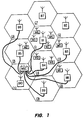
- FIG. 1 there is illustrated a digital cellular radio system including mobile station radios which implement the frequency stabilization system of the present invention.
- FIG. 1 illustrates ten cells C1-C10, each of which includes a base station B1-B10, respectively.
- FIG. 1 also illustrates ten mobile stations M1-M10 which are moveable within a cell and from one cell to another cell within the system.
- a mobile switching center MSC which is connected to all ten of the illustrated base stations (B1-B10) by means of electrical connections such as the cable shown.
- the mobile switching center may also be connected to a fixed public switching telephone network or similar fixed private network (not shown).
- the mobile system illustrated in FIG. 1 comprises at least one duplex radio channel and preferably a plurality of duplex radio channels for communication between the various base stations and the mobiles.
- each base station has its own duplex radio channel (pair of simplex radio channels) or its own allotted time on a duplex radio channel (pair of simplex radio channels) for communication with mobile stations served by that base station.
- two or more base stations may cooperate in certain procedures, e.g., handoff or roaming, it will, for the purpose of explaining the present invention, be sufficient to consider only the communication between one base station, e.g., B1, and one of the mobile stations served by that particular base station, e.g., M3, M4, M6 and M7.
- one base station e.g., B1
- one of the mobile stations served by that particular base station e.g., M3, M4, M6 and M7.
- FIG. 2 illustrates a block diagram of a mobile station within the system of FIG. 1
- FIG. 3 illustrates a block diagram of a base station within FIG. 1, each for possible use in connection with the system of the present invention.
- the base and mobile stations are designed for full duplex digital message communications in time slots of a radio channel that may be shared by plural mobile stations within plural mobile systems of a network.
- a base station normally comprises means for enabling it to simultaneously communicate on more than one radio channel only means for communications on one radio channel is illustrated in FIG. 3.
- Both base and mobile stations comprise a micro-processor control radio receiver. Referring to both FIGS. 2 and 3, the radio transmitter 10 transmits radio signals modulated with digital messages generated by a message generator 11.
- the message generator is connected to a data information source 12, e.g., a keyboard, via a data information buffer 13.
- the information to be transmitted in both the mobile and the base stations is processed by means of a data modulator and a data signal processor.
- the message generator and data information buffer 12 is connected to a data line terminal 14 receiving data from a data network to which the data terminal is connected by circuits such as fixed telephone lines.
- the message decoder 18 is connected to a data information output means 15, e.g., the display, via data information buffer 16.
- the message decoder 18 is instead connected via data information buffer 16 to a data line terminal 17 supplying data to a data network to which the data terminal is connected by circuits such as fixed telephone lines.
- Transmitted information received by the receiver 19 of both the base and the mobile stations is processed by an audio output processor 26 and a data demodulator 27.
- the radio channel on which the radio transmitters and receivers of both the mobile and base stations operate is determined by frequencies supplied from a frequency synthesizer 20 controlled by the micro-processor 21.
- the base and mobile both include means 22 for storing algorithms, codes, rules, formats, data and compensation values.
- the digital packet radio system of the present invention maintains its communications in accordance with a prescribed signaling protocol which includes a logical structure of data controlling the communication between each base station and the mobile stations.
- a prescribed signaling protocol which includes a logical structure of data controlling the communication between each base station and the mobile stations.
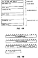
- each burst of transmitted information from the base station to a mobile includes a framehead 31 which is followed by other control information and data, a primary block 32 and additional data blocks 33, each of which includes a parity field 34 for error detection and correction.
- the protocol format of each framehead for each transmitted packet is the same.
- Figure 4B illustrates the arrangement of the data comprising the framehead showing that bits 1-16 comprise the bit synchronization block 34, bits 17-32 comprise the frame synchronization block 35, while bits 33-38, 39-44, and 45-48 comprise the base identity 36, area identity 37, and control flag blocks 38 and bits 49-56 comprise parity bits 39 used in the error correction system of the radio.
- the bit synchronization block 34 always includes the same pattern of ones and zeros which enables an accurate measurement of the transmitted frequency as will be further discussed below.
- the base identity and area identity blocks 36 and 37 together identify the particular base station so that upon receipt, the mobile can ensure that the signal received is from the particular current base station of the mobile prior to measuring the received signal as will be described below.
- the remainder of the frame of digital information transmitted over the radio channel following the framehead is the primary block 32 which includes the mobile station address and other information and a parity field 34. Thereafter, information fields 33, a sequence of blocks of information comprising an information field and a parity field 34, are broadcast until the required information has been transmitted.
- the mobile stations within the system of the present invention operate within an environment in which radio channels are shared within a network between more than one operator and, thus, it is essential that a mobile which is to use a signal transmitted from a base station as its frequency stability standard use only its own base station for such purpose.
- the transmitters of the present system operate in burst mode and, as a result, a mobile station only has a very short time period in which to take measurements of the signal transmitted from a base station.
- the system requires a high degree of frequency stability within both its transmitter and its receiver.
- the mobile stations within the system operate within a frequency stability standard of about ⁇ 1.5 PPM ( ⁇ 1.35 KH z at 900 MH z ). For this reason, there must be a high level of stability within the reference oscillators of the radio circuits. In most cases, such a high level frequency stability is only obtainable through use of oven control crystal oscillators. However, mobile stations cannot, for reasons of both size and cost, obtain frequency stability in this way.
- the method and circuit of the present invention enables a very high degree of reference crystal frequency stability within a mobile unit without temperature control of the reference oscillator.
- the system of the present invention involves three basic components which contribute to frequency stability of the crystal within the reference frequency oscillator: (a) temperature component; (b) aging component; and (c) modulation voltage component.
- the temperature component of crystal frequency stability relates to the fact that the resonant frequency of a crystal changes as a function of the temperature of the crystal.
- the crystal reference oscillator of a mobile station within the system of the present invention is calibrated during manufacture by receiving a reference carrier signal and cycling the radio through the entire range of temperature conditions under which it is intended to operate. At each incremental value of temperature, there is determined the specific value of compensation voltage which is necessary to cause the crystal to operate at the desired frequency at that specific temperature. In this way, a series of voltages are stored in a look-up table, one voltage for each value of temperature, within a memory of the radio to be recalled as a temperature compensation value to be used when the radio is operating at that particular temperature.
- the aging component of the crystal frequency stability relates to the fact that as a crystal ages over time, its resonant frequency changes.
- the system of the present invention compensates for crystal aging by measuring the output frequency of the crystal with the temperature compensation voltage applied and then comparing that output signal to the received standard frequency from the base station. If the frequency of the crystal within the mobile has varied from its desired value, an aging compensation voltage is introduced which causes the crystal to return to the same frequency as that of the base station transmitter which is used as the standard.
- the aging component of crystal frequency voltage compensation simply shifts the temperature compensation curve in one direction or another but does not change the shape of that curve.
- the modulation voltage component of crystal frequency stability relates to the fact that the resonant frequency of the crystal varies as a function of the tuning voltage which is applied to the crystal oscillator. As that modulation voltage changes, it changes the shape of variations in the crystal's output frequency as a function of temperature.
- the temperature compensation values are stored as voltage values in a memory within the radio based upon a calibration routine performed when the radio is manufactured.
- the aging compensation values of the crystal vary as a function of the voltage applied to the reference oscillator.
- the aging compensation value is stored as a value of frequency deviation but before it is applied to correct the crystal, it is converted to a voltage based upon the voltage-to-frequency relationship of that particular reference oscillator.
- a test of change in frequency as a function of voltage for the particular radio circuit is run and that is stored in memory.
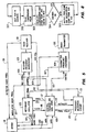
- FIG. 5 there is shown a block diagram of a mobile radio station frequency compensation system constructed in accordance with the teachings of the present invention.
- a radio receiver 101 and a radio transmitter 102 are each connected, respectively, to a receiver frequency synthesizer 103 and a transmitter frequency synthesizer 104, each of which operate in accordance with standard phase locked loop frequency synthesization circuitry.
- Both the receiver frequency synthesizer 103 and the transmitter frequency synthesizer 104 receive a reference frequency from a reference oscillator 105 which includes a reference crystal, the resonant frequency of which is stabilized in accordance with the system of the present invention.
- the reference frequency is connected to the receiver frequency synthesizer 103 via line 106 and to the transmitter frequency synthesizer 104 via line 107.
- the receiver frequency synthesizer 103 and transmitter frequency synthesizer 104 are operated under control of a control, program and data store module 108, which includes a micro-processor and a memory, and is connected to the two synthesizers 103 and 104 by means of control lines 109 and 110, respectively.
- a frequency measuring circuit 111 receives a reference frequency from the reference oscillator 105 via line 112 and a standard reference signal is received from the transmitter of the base station (not shown) by the radio receiver 101 and which is connected to the frequency measuring circuit 111 via line 113.
- the base station transmitter signal is used in the form of a second IF frequency of 450 KH z .
- the control, program and data store module 108 is connected to the frequency measuring circuit 111 to provide an initialization signal on line 114 and to receive a measured frequency value on line 115.
- the module 108 is also connected to the reference oscillator 105 to receive a clock signal, derived from the reference frequency signal, on line 116.
- the module 108 also provides a frequency adjustment signal on line 117 to change the value of the reference frequency being generated by the reference oscillator in accordance with the results of the frequency measuring circuit 111 and its comparison of the reference frequency to the standard signal received from the base station transmitter.
- a modem 118 receives a detected audio frequency from the radio receiver 101 via line 119 and provides a modulated audio frequency signal to the transmitter frequency synthesizer 104 via line 121.
- the modem 118 receives data from the control, program and data store module 108 via line 122 and sends data to the module 108 via line 123.
- the modem also provides a moduled audio frequency signal to the reference oscillator 105 on line 124 and to the transmitter frequency synthesizer 104 on line 121.
- the reference oscillator compensation circuitry of FIG. 5 functions as follows:
- the 450 KH z signal is used to provide a one milli-second gating signal during which time the cycles of the reference frequency on line 112 from the reference oscillator 105 are counted in a counter.
- the number of cycles of this signal counted during the one milli-second time period is used as the value from which is determined the aging compensation value which should applied to crystal within the reference oscillator 105 to provide a stable frequency output.
- the control, program and data store module 108 provides a frequency adjustment signal on line 117 based upon three parameters. First, a stored voltage representing a temperature compensation value for the crystal within the reference oscillator and which is based upon the temperature at which the oscillator is operating. Second, the module 108 supplies an aging component frequency compensation to the crystal within the reference oscillator 105 based upon the comparison between the reference frequency on line 112 and the period of the signal from the base station transmitter on line 113. This is done by using the base station signal on line 113 to provide a pair of gating pulses during which the number of cycles of the reference frequency on line 113 are counted.
- the control module 108 determines whether or not the reference frequency signal on line 112 is within the prescribed frequency range and, if not, adds a voltage component to correct for the aging of the crystal which has occurred and effectively shift the temperature compensation value in order to compensate for the aging of the crystal.
- the control module 108 receives data from the modem 118 on line 123 indicative of the modulation voltage on line 124. This enables the frequency adjustment voltages on line 117 to be varied to account for the modulation voltage component and adjust for the aging of the crystal as a function of the modulation voltage which is applied to the reference oscillator 105.
- the receiver 101 includes a receiving antenna 131, a first mixer 132, a second mixer 133 and a detector 134.
- the receiver's frequency synthesizer 103 includes a conventional receiver local oscillator circuit comprising a phase locked-loop circuit including phase detector 135, a loop filter 136 and a voltage controlled oscillator 137.
- the transmitter 102 includes a transmitting antenna 141 and the transmitter frequency synthesizer 104 includes a relatively standard transmitter local oscillator circuit comprising a phase locked-loop circuit including phase detector 142, a loop filter 143 and a voltage controlled oscillator 144.
- Both the receiver local oscillator 103 and the transmitter local oscillator 104 receive a reference frequency signal from the reference oscillator 105 which includes the reference crystal 146, the frequency stability of which is being compensated in the system of the present invention and a thermally sensitive measuring device 147, such as a thermistor, which produces an output signal on line 152 indicative of the temperature at which the reference oscillator 105 is operating.
- the 12.8 MH z reference frequency output signal of the reference oscillator is connected to the receiver frequency synthesizer 103, the transmitter frequency synthesizer 104 and the second mixer 133 of the receiver 101 through a times 6 frequency multiplier 148.
- the output signal from the thermally sensitive device 147 is coupled to a multiplexing analog-to-digital converter 151 via line 152 while the received signal strength signal (RSSI) is connected from the detector 134 in the receiver 101 to the multiplexing A/D converter on line 153 and data is connected from the detector 134 on line 154.
- the output of the multiplexing A/D converter 151 is connected to a dual-port RAM memory 155 through a bus structure 156 and from there to the control micro-processor 157 through its bus structure 158.
- a signal processor 159 which serves primarily as a modem, is connected to both the double-port RAM 155 and a D/A converter 161 via the bus structure 156.
- a memory 162 is coupled to the micro-processor and other components via the bus structure 158.
- a modulation compensation digital-to-analog converter 163 receives an input from the bus structure 158 and is connected to provide a modulation compensation voltage to the D/A converter 161.
- a digital-to-analog converter 164 is connected to receive an input from the bus structure 158 and provide an output temperature compensation voltage to an operational amplifier 165.
- the output of the operational amplifier 165 provides an oscillator control signal on line 166 to apply the compensation voltage to the reference oscillator 145 and stabilize its output signal.
- a first counter 167 receives a 450 K z IF signal from the detector 134 within the receiver 101 and provides a gating signal over line 168 to a second counter 169.
- the counter 167 provides an interrupt signal on line 171 to the micro-processor 157.
- Both the first and second counters 167 and 169 receive inputs on the micro-processor bus structure 158.
- the reference frequency, 12.8 MH Z from the reference oscillator 105, is connected through a times 3 multiplier circuit 172, a divide by 8 divider circuit 173 and a divide by 4 divider circuit 174 to produce a 4.8 MH z signal to one input of the second counter 169.
- the 4.8 MH z output signal from the divide by 4 divider 174 is connected to the micro-processor 157 as a 4.8 MH z clock signal while the output of the divide by 8 divider circuit 173 is connected to provide a 19.2 MH z clock signal to the signal processor 159.
- the signal processor 159 serves as a modem to generate modulation within the radio transmitter and to receive and detect transmitted data received from the detector 134 via the line 154 and the multiplexing analog converter 151.
- the DP RAM 155 is a double-port RAM memory which is used as temporary storage for communication between the signal processor 159 and the micro-processor 157.
- the micro-processor 157 controls the radio and runs the various algorithms which perform calculations and control functions within the radio.
- the memory 162 includes both ROM and RAM types of memory and stores the various data tables used in frequency compensation in accordance with the system of the present invention.
- the multiplexing A/D converter 151 receives the various analog signals and multiplexes them into the bus structure 156.
- the signals include the receive signal strength indicator (RSSI) signals from detector 134 and audio frequency data on line 154 from detector 134 along with the temperature signal from the thermistor 147 within the reference oscillator 105.
- the multiplexer 151 converts the audio signals to digital and then multiplexes the data from each of the three inputs into the data bus 156 for communication with the DP RAM 155 and the micro-processor 157.
- the digital-to-analog converter 161 is part of the modulation voltage compensation system in the present system.
- a modulation voltage comes in from the signal processor 159 which produces a modulation compensation voltage to the input of the summing amplifier 165.
- the digital-to-analog converter 163 controls the gain through a reference voltage applied on line 170 to the digital-to-analog converter 161.
- the summation amplifier 165 receives signals from both of the digital-to-analog converters 161 and 164 and outputs an oscillator control signal on line 166 to the reference oscillator 105.
- the digital-to-analog converter 164 converts the digital values stored in memory 162 (from the look-up table stored during calibration) into an analog signal and applies that signal as a temperature compensation voltage to the summing amplifier 165.
- the value input to the digital-to-analog converter 164 has also been compensated for aging and gain related variations, just like the modulation voltage compensation discussed above. This value is output by the digital-to-analog converter 164 as a function of the aging compensation value measured in another part of the circuit.
- the first counter of 167 gives a nominal one milli-second output pulse via line 168 to the second counter 169.
- Counter 169 counts the number of cycles of the 4.8 MH z signal which occur during the one milli-second gating pulses received from the first counter. This is then used as a measure of the frequency of the carrier signal received from the base station by the receiver 101. This frequency deviation value from the standard established by the base station transmitter is used to obtain the aging compensation to be applied to the crystal 146 within the oscillator 105.
- the dividers/multipliers 172, 173 and 174 process the reference frequency signal from the reference oscillator 105 to give a 4.8 MH z signal which goes both to the micro-processor 157 as a clock and to the second counter 169 as a representation of the reference frequency signal.
- the signal received from the base station on antenna 131 is combined in the first mixer 132 with the signal from local oscillator 103 to produce a 75.25 MH z signal which is introduced to the second mixer 133 along with a 76.8 MH z signal, obtained from the reference oscillator by a times 6 multiplication circuit 148, to produce an output signal of 450 KH z to the detector 134.
- the 450 KH z IF signal on line 160 is connected to the input of the first counter 167 which counts 900 cycles and provides gating signals with a nominal one milli-second separation between them.
- the output of the reference oscillator 105 is multiplied and divided in circuits 172, 173 and 174 to produce a 4.8 MH z signal as an input to the second counter 169.
- the signal output from the first counter 167 to the second counter 169 on line 168 is a square-wave pulse having a nominal one milli-second period.
- the second counter 169 will count 4,800 pulses from the 4.8 MH z signal during the one milli-second period.
- the value actually counted by the second counter 169 is sent to the microprocessor 157 and the memory 162 via the bus structure 158.
- the micro-processor 157 determines the degree of deviation of the output signal of the reference oscillator 105 and adds an aging compensation voltage correction to the temperature compensation voltage stored in memory 162 and applies that value to the digital-to-analog converter 164.
- a value is received by the digital-to-analog converter 161, which represents the modulation voltage from the signal processor 159, along with a reference value voltage from the digital-to-analog converter 163, which represents a modulation compensation offset voltage, on line 170 to produce an analog output voltage to the summing amplifier 165.
- a composite oscillator control signal 166 is applied to the reference oscillator 103 to maintain the output reference frequency as near to the desire standard frequency value as possible.
- the system measures a frequency value, as described above in connection with FIG. 6, during the approximate one milli-second burst of RF energy transmitted from the base station in the burst mode operation.
- the system makes the frequency measurement only during the time when it is receiving the bit synchronization block portion of the framehead to insure that the received frequency is used as a standard only during the consistent pattern of ones and zeros comprising each bit synchronization block. Since the pattern of data with which the transmitted signal is modulated effects the nominal frequency of the transmitted signal this consistent pattern of transmitted information insures greater accuracy within the measurements.
- the system determines whether or not the bit synchronization block was found within the signal which was measured. If not, the system recycles to 201 to measure again and if so, it moves to 203 to store the measured frequency value in memory.
- the system determines whether the entire framehead of the transmitted burst has been received from the base station. The framehead portion of the transmitted data block contains the base identity block and the area identity block which together identify the particular base station transmitting the information. Once the system determines at 204 that a framehead has been received, it determines at 205 whether a complete frame has been received. The entire frame includes a parity field of data which enables the system to determine whether or not there are any data errors occurring in the transmission.
- the system determines whether there is less than the maximum error in the received data so that the received data can be used to ascertain whether the correct base station has been received. If the data is determined to be of sufficient accuracy at 206, the system determines at 207 whether the signal measured at 201 was from the current base station of the mobile station doing the measuring.
- the system determines whether or not the difference error between the frequency measured at 201 and the reference frequency within the reference oscillator, frequency error X, is less than a maximum allowable error value.
- a maximum allowable error value might typically be on the order of 5 KH z . If the error was greater than the maximum allowable then the system automatically disables the transmitter of the mobile unit at 209 and prevents any additional transmission of signal from it. This prevents transmission of signals by a mobile station which would be out of its assigned frequency channel and cause serious problems within both the radio system and the network.
- the system moves to 210 where it determines whether or not the error was less than the maximum operating error allowable without correction. If not, the transmitter is again disabled at 211 but if so, the transmitter continues to remain enabled at 212. At a nominal carrier frequency of 900 MH z the maximum operating error might typically be on the order of 1.5 KH z . In effect, steps 208 and 210 amount to a double check on the frequency error of the reference oscillator. Any exceedingly gross errors are limited in 208 and more subtle operating errors are accounted for in 210.
- the algorithm run at 213 is to avoid large incremental jumps in aging compensation value but rather include a slow and steady correction of the aging variations over a period of several sequential measurements.
- the previously determined (and currently used) value of aging compensation, Y n remains stored in permanent memory (Y perm ).
- FIG. 8 there is shown a flow chart of the control program of the frequency stabilization compensation of the present system.
- the system waits for a pre-selected number of N seconds and then reads the temperature value of the thermistor contained within the reference oscillator at 302.
- the system calculates the compensation voltage to be applied to the crystal from both the temperature component and the aging component (as well as the modulation voltage component discussed above), as set forth in the flow chart of FIG. 7, and determines the voltage compensation factor to be applied to the crystal.
- the system determines whether or not the carrier of the transmitter of the mobile station is on.
- the system again returns to 301 to wait for X seconds and cycles it again.
- the system moves to 305 at which the output temperature voltage compensation, aging voltage compensation and modulation voltage compensation from the various D/A converters is applied to the reference oscillator to insure that the output signal therefrom is within the desired frequency stability range of the system.
Landscapes
- Engineering & Computer Science (AREA)
- Computer Hardware Design (AREA)
- Microelectronics & Electronic Packaging (AREA)
- Mobile Radio Communication Systems (AREA)
- Oscillators With Electromechanical Resonators (AREA)
- Transmitters (AREA)
Claims (22)
- System zum Erzeugen einer Frequenzkompensationsspannung für einen Kristall-gesteuerten Referenzoszillator in einer mobilen Station eines Paketdaten-Funksystems, umfassend:eine erste Einrichtung (162) zum Speichern einer Folge von Spannungswerten, die jeweils einer Temperaturkompensationsspannung entsprechen, die an den Referenzoszillator bei einer bestimmten Temperatur angelegt werden soll, um ein Referenzfrequenzsignal bei einer bestimmten Frequenz zu erzeugen;eine Einrichtung (147) zum Messen der gegenwärtigen Temperatur des Referenzoszillators;eine Einrichtung (157, 164) zum Wählen der Temperaturkompensationsspannung entsprechend der gemessenen Temperatur von der ersten Speicherungseinrichtung und zum Anlegen der Spannung an den Referenzoszillator;eine Einrichtung (101, 103) zum Empfangen eines Bursts von übertragenen Daten von einer Basisstation;eine Einrichtung (157, 167, 169) zum Vergleichen der Frequenz des von der Basisstation empfangenen Signals mit der Frequenz des Signalausgangs von dem Referenzoszillator zum Erzeugen eines Differenzsignals;eine zweite Einrichtung (162) zum Speichern eines Kristall-Alterungskompensationswerts, der die Differenz zwischen der Frequenz des Referenzoszillator-Ausgangssignals und der Differenz des von der Basisstation empfangenen Signals anzeigt; undgekennzeichnet durcheine Einrichtung (157) zum Bestimmen, ob der Burst von empfangenen übertragenen Daten durch die gegenwärtige Basisstation der mobilen Station gesendet wurde; undeine Einrichtung (157, 164), die auf eine Bestimmung anspricht, daß die Basisstation, von der das Signal empfangen wurde, die gegenwärtige Basisstation der mobilen Station ist, zum Modifizieren der gewählten Temperaturkompensationsspannung gemäß dem Alterungskompensationswert in der zweiten Speicherungseinrichtung und zum Anlegen der modifizierten Spannung an den Referenzoszillator, um die gleiche Frequenz zu erzeugen, wie diejenige, die von der Basisstation empfangen wird.
- System zum Erzeugen einer Frequenzkompensationsspannung für einen Kristall-gesteuerten Referenzoszillator in einer mobilen Station eines Paketdaten-Funksystems nach Anspruch 1, wobei die Frequenzvergleichseinrichtung umfaßt:eine Einrichtung zum Zählen einer vorgewählten Anzahl von Zyklen eines Signals, welches von dem Signal abgeleitet ist, welches von der Basisstation empfangen wird, und zum Erzeugen eines periodischen Schaltsignals;eine Einrichtung zum Zählen der Anzahl von Zyklen eines Signals, welches von dem Referenzoszillatorsignal abgeleitet ist, welches zwischen aufeinanderfolgenden Schaltsignalen auftritt; undeine Einrichtung zum Vergleichen der gezählten Anzahl von Zyklen mit einem Wert, der sich auf die Frequenz bezieht, die von der Basisstation empfangen wird, um den Wert zu bestimmen, der die Differenz anzeigt.
- System zum Erzeugen einer Frequenzkompensationsspannung für einen Kristall-gesteuerten Referenzoszillator in einer mobilen Station eines Paketdaten-Funksystems nach Anspruch 1, ferner umfassend:eine dritte Einrichtung zum Speichern einer Folge von Werten, die die Veränderung einer Frequenz des Kristalloszillators als eine Funktion einer an den Oszillator angelegten Abstimmspannung darstellen;eine Einrichtung zum Messen der an den Kristalloszillator angelegten Abstimmspannung;eine Einrichtung zum Wählen eines Werts von der dritten Speicherungseinrichtung entsprechend der an den Kristalloszillator angelegten gemessen Abstimmspannung;eine Einrichtung zu weiteren Modifizierung der Kristalltemperatur- und Kristallalterungskompensationsspannungen von den ersten und zweiten Speicherungseinrichtungen gemäß dem von der dritten Speicherungseinrichtung gewählten Wert und zum Anlegen der weiter modifizierten Spannung an den Kristall des Referenzoszillators, um die Frequenz zu ermitteln, die von der Basisstation empfangen wird.
- System zum Erzeugen einer Frequenzkompensationsspannung für einen Kristall-gesteuerten Referenzoszillator in einer mobilen Station eines Paketdaten-Funksystems nach Anspruch 1, ferner umfassend:eine Einrichtung zum Bestimmen, wenn ein vollständiger Datenrahmen innerhalb des Bursts von Daten, die von der Basisstation gesendet werden, empfangen worden ist;eine Einrichtung zum Bestimmen, ob die empfangenen Daten mehr als eine vorgewählte Anzahl von Datenfehlern enthalten, bevor die Vergleichseinrichtung betrieben wird.
- System zum Erzeugen einer Frequenzkompensationsspannung für einen Kristall-gesteuerten Referenzoszillator in einer mobilen Station eines Paketdaten-Funksystems nach Anspruch 4, bei dem der Burst von Daten, die von der Basisstation gesendet werden, gemäß einem Protokoll formatiert ist, welches umfaßt:einen Bitsynchronisationsblock mit einer festen Konfiguration von Daten;einen Rahmenanfangsblock mit einem Basisstationsidentitätsblock; undein Paritätsfeld, welches Information für eine Fehlerkorrektur umfaßt.
- System zum Erzeugen einer Frequenzkompensationsspannung für einen Kristall-gesteuerten Referenzoszillator in einer mobilen Station eines Paketdaten-Funksystems nach Anspruch 5, in dem
die Vergleichseinrichtung eine Einrichtung umfaßt, um die Frequenz des Signals zu vergleichen, welches von der Basisstation während dem Abschnitt des Bursts, der den Bitsynchronisationsblock enthält, empfangen wird. - System zum Erzeugen einer Frequenzkompensationsspannung für einen Kristall-gesteuerten Referenzoszillator in einer mobilen Station eines Paketdaten-Funksystems nach Anspruch 5, wobei:
die Einrichtung zum Bestimmen, ob der Burst von empfangenen gesendeten Daten durch die gegenwärtige Basisstation der mobilen Station übertragen wurde, eine Einrichtung umfaßt, um den Basisstationsidentitätsblock innerhalb des Rahmenanfangsblocks des Datenbursts zu erkennen. - System zum Erzeugen einer Frequenzkompensationsspannung für einen Kristall-gesteuerten Referenzoszillator in einer mobilen Station eines Paketdaten-Funksystems nach Anspruch 1, welches ferner umfaßt:eine Einrichtung zum Vergleichen des Kristall-Alterungskompensationswerts, der vorher in der zweiten Speicherungseinrichtung gespeichert wurde, mit dem gegenwärtigen Kristallkompensationswert;eine Einrichtung zum Bestimmen der Differenz zwischen den Kristall-Alterungskompensationswerten; undeine Einrichtung, die auf die einen vorgewählten Wert übersteigende Differenz entspricht, zum Speichern eines neuen Kristall-Alterungskompensationswerts in der zweiten Speicherungseinrichtung.
- System zum Erzeugen einer Frequenzkompensationsspannung für einen Kristall-gesteuerten Referenzoszillator in einer mobilen Station eines Paketdaten-Funksystems nach Anspruch 8, wobei:
die Einrichtung zum Speichern eines neuen Kristall-Alterungskompensationswerts eine Einrichtung umfaßt, um einen Bruchteil der Differenz zwischen den Alterungskompensationswerten zu dem vorher gespeicherten Alterungskompensationswert hinzu zu addieren, um den neuen zu speichernden Kristall-Alterungskompensationswert zu erhalten. - System zum Erzeugen einer Frequenzkompensationsspannung für einen Kristall-gesteuerten Referenzoszillator in einer mobilen Station eines Paketdaten-Funksystems nach Anspruch 1, welches ferner umfaßt:
eine Einrichtung, die auf die einen vorgewählten Wert übersteigende Differenz zwischen der Frequenz des von der Basisstation empfangenen Signals und der Frequenz des von dem Referenzoszillator ausgegebenen Signals anspricht, um den Betrieb des Senders der mobilen Station zu sperren. - System zum Erzeugen einer Frequenzkompensationsspannung für einen Kristall-gesteuerten Referenzoszillator in einer mobilen Station eines Paketdaten-Funksystems nach Anspruch 2, wobei:
das Signal, welches von dem Signal abgeleitet ist, das von der Basisstation empfangen wird, eine Zwischenfrequenz davon ist. - Verfahren zum Erzeugen einer Frequenzkompensationsspannung für einen Kristall-gesteuerten Referenzoszillator in einer mobilen Station eines Paketdaten-Funksystems, umfassend:Speichern einer Folge von Spannungswerten an einer ersten Stelle, die jeweils der Temperaturkompensationsspannung entsprechen, die an den Referenzoszillator bei einer bestimmten Temperatur angelegt werden soll, um ein Referenzfrequenzsignal bei einer bestimmten Frequenz zu erzeugen;Messen der gegenwärtigen Temperatur des Referenzoszillators;Wählen der Temperaturkompensationsspannung entsprechend der gemessenen Temperatur von der ersten Speicherungseinrichtung und Anlegen der Spannung an den Referenzoszillator;Empfangen eines Bursts von gesendeten Daten von einer Basisstation;Vergleichen der Frequenz des von der Basisstation empfangenen Signals mit der Frequenz des von dem Referenzoszillator ausgegebenen Signals und Erzeugen eines Differenzsignals;Speichern an einer zweiten Stelle eines Kristall-Alterungskompensationswerts, der die Differenz zwischen der Frequenz des Referenzoszillatorausganggssignals und der Frequenz des von der Basisstation empfangenen Signals anzeigt; undgekennzeichnet durch die folgenden Schritte:Bestimmen, ob der Burst von empfangenen gesendeten Daten von der gegenwärtigen Basisstation der mobilen Station empfangen wurde; undModifizieren der gewählten Temperaturkompensationsspannung gemäß dem Alterungskompensationswert an der zweiten Speicherungsstelle im Ansprechen auf eine Bestimmung, daß die Basisstation, von der das Signal empfangen wurde, die gegenwärtige Basisstation der mobilen Einrichtung war und Anlegen der modifizierten Spannung an den Referenzoszillator, um die gleiche Frequenz wie diejenige zu erzeugen, die von der Basisstation empfangen wurde.
- Verfahren zum Erzeugen einer Frequenzkompensationsspannung für einen Kristall-gesteuerten Referenzoszillator in einer mobilen Station eines Paketdaten-Funksystems nach Anspruch 11, wobei der Frequenzvergleichsschritt umfaßt:Zählen einer vorgewählten Anzahl von Zyklen eines Signals, welches von dem Signal abgeleitet ist, das von der Basisstation empfangen wird und Erzeugen eines periodischen Schaltsignals;Zählen der Anzahl von Zyklen eines Signals, welches von dem Referenzoszillatorsignal abgeleitet ist, das zwischen aufeinanderfolgenden Schaltsignalen auftritt; undVergleichen der gezählten Anzahl von Zyklen mit einem Wert, der sich auf die Frequenz bezieht, die von der Basisstation empfangen wird, um den Wert zu bestimmen, der die Differenz anzeigt.
- Verfahren zum Erzeugen einer Frequenzkompensationsspannung für einen Kristall-gesteuerten Referenzoszillator in einer mobilen Station eines Paketdaten-Funksystems nach Anspruch 12, welches ferner die folgenden Schritte umfaßt:Speichern einer Folge von Werten an einer dritten Stelle, die die Veränderung einer Frequenz des Kristalloszillators als eine Funktion einer an den Oszillator angelegten Abstimmspannung darstellen;Messen der an den Kristalloszillator angelegten Abstimmspannung;Wählen eines Werts von der dritten Speicherungsstelle entsprechend der gemessenen Abstimmspannung, die an den Kristalloszillator angelegt ist;weiteres Modifizieren der Kristalltemperatur- und Kristall-Alterungskompensationsspannungen von den ersten und zweiten Speicherungsstellen entsprechend dem Wert, der von der dritten Speicherungsstelle gewählt wird, und Anlegen der weiter modifizierten Spannung an den Referenzoszillator, um die von der Basisstation empfangene Frequenz zu erhalten.
- Verfahren zum Erzeugen einer Frequenzkompensationsspannung für einen Kristall-gesteuerten Referenzoszillator in einer mobilen Station eines Paketdaten-Funksystems nach Anspruch 12, ferner umfassend die folgenden Schritte:Bestimmen, wenn ein vollständiger Datenrahmen innerhalb des Bursts von Daten, der von der Basisstation übertragen wird, empfangen worden ist;Bestimmen, ob die empfangenen Daten mehr als eine vorgewählte Anzahl von Datenfehlern enthalten, vor dem Vergleichsschritt.
- Verfahren zum Erzeugen einer Frequenzkompensationsspannung für einen Kristall-gesteuerten Referenzoszillator in einer mobilen Station eines Paketdaten-Funksystems nach Anspruch 15, wobei der Burst von Daten, der durch die Basisstation übertragen wird, gemäß einem Protokoll formatiert ist, welches umfaßt:einen Bitsynchronisationsblock mit einer festen Konfiguration von Daten;einen Rahmenanfangsblock mit einem Basisstationsidentitätsblock; undein Paritätsfeld, welches Information für eine Fehlerkorrektur umfaßt.
- Verfahren zum Erzeugen einer Frequenzkompensationsspannung für einen Kristall-gesteuerten Referenzoszillator in einer mobilen Station eines Paketdaten-Funksystems nach Anspruch 16, wobei der Vergleichsschritt umfaßt:
Vergleichen der Frequenz des Signals, welches von der Basisstation während des Abschnitts des Bursts, der den Bitsynchronisationsblock enthält, empfangen wird. - Verfahren zum Erzeugen einer Frequenzkompensationsspannung für einen Kristall-gesteuerten Referenzoszillator in einer mobilen Station eines Paketdaten-Funksystems nach Anspruch 16, wobei:
der Schritt zum Bestimmen, ob der Burst von empfangenen übertragenen Daten von der gegenwärtigen Basisstation der mobilen Station übertragen wurde, eine Erkennung des Basisstationsidentitätsblocks in dem Rahmenanfangsblock des Datenbursts umfaßt. - Verfahren zum Erzeugen einer Frequenzkompensationsspannung für einen Kristall-gesteuerten Referenzoszillator in einer mobilen Station eines Paketdaten-Funksystems nach Anspruch 12, ferner umfassend die folgenden Schritte:Vergleichen des Kristall-Alterungskompensationswerts, der vorher an der zweiten Speicherungsstelle gespeichert wurde, mit dem gegenwärtigen Kristallkompensationswert;Bestimmen der Differenz zwischen den Kristall-Alterungskompensationswerten; undSpeichern eines neuen Kristall-Alterungskompensationswerts an der zweiten Speicherungsstelle im Ansprechen auf die einen vorgewählten Wert übersteigende Differenz.
- Verfahren zum Erzeugen einer Frequenzkompensationsspannung für einen Kristall-gesteuerten Referenzoszillator in einer mobilen Station eines Paketdaten-Funksystems nach Anspruch 19, wobei:der Schritt des Speicherns eines neuen Kristall-Alterungskompensationswerts umfaßt:Addieren eines Bruchteils der Differenz zwischen den Alterungskompensationswerten zu dem vorher gespeicherten Alterungskompensationswert, um den neuen Kristall-Alterungskompensationswert zu ermitteln, der gespeichert werden soll.
- Verfahren zum Erzeugen einer Frequenzkompensationsspannung für einen Kristall-gesteuerten Referenzoszillator in einer mobilen Station eines Paketdaten-Funksystems nach Anspruch 12, ferner umfassend den folgenden Schritt:
Sperren des Betriebs des Senders der mobilen Station im Ansprechen auf die Tatsache, daß die Differenz zwischen der Frequenz des von der Basisstation empfangenen Signals und der Frequenz des von dem Referenzoszillator ausgegebenen Signals einen vorgegebenen Wert übersteigt. - Verfahren zum Erzeugen einer Frequenzkompensationsspannung für einen Kristall-gesteuerten Referenzoszillator in einer mobilen Station eines Paketdaten-Funksystems nach Anspruch 13, wobei:
das Signal, welches von dem Signal abgeleitet ist, welches von der Basisstation empfangen wird, eine Zwischenfrequenz davon ist.
Applications Claiming Priority (2)
| Application Number | Priority Date | Filing Date | Title |
|---|---|---|---|
| US07/604,141 US5113416A (en) | 1990-10-26 | 1990-10-26 | Digital radio frequency compensation |
| US604141 | 1996-02-20 |
Publications (2)
| Publication Number | Publication Date |
|---|---|
| EP0483090A1 EP0483090A1 (de) | 1992-04-29 |
| EP0483090B1 true EP0483090B1 (de) | 1996-03-27 |
Family
ID=24418339
Family Applications (1)
| Application Number | Title | Priority Date | Filing Date |
|---|---|---|---|
| EP91850256A Expired - Lifetime EP0483090B1 (de) | 1990-10-26 | 1991-10-18 | Digitale Hochfrequenzkompensation |
Country Status (8)
| Country | Link |
|---|---|
| US (1) | US5113416A (de) |
| EP (1) | EP0483090B1 (de) |
| AU (1) | AU635693B2 (de) |
| CA (1) | CA2054237C (de) |
| DE (1) | DE69118311T2 (de) |
| ES (1) | ES2087988T3 (de) |
| FI (1) | FI105618B (de) |
| HK (1) | HK132296A (de) |
Families Citing this family (56)
| Publication number | Priority date | Publication date | Assignee | Title |
|---|---|---|---|---|
| JPH0422225A (ja) * | 1990-05-17 | 1992-01-27 | Sony Corp | 通信方式 |
| GB2254971B (en) * | 1991-03-07 | 1994-12-21 | Ericsson Telefon Ab L M | Mobile radio communications stations |
| US5287388A (en) * | 1991-06-25 | 1994-02-15 | Kabushiki Kaisha Toshiba | Frequency offset removal method and apparatus |
| US5289504A (en) * | 1991-06-28 | 1994-02-22 | Wilson Timothy J | Signal decoding method using both signal and channel state information |
| JP3381870B2 (ja) * | 1992-11-30 | 2003-03-04 | ヒューレット・パッカード・カンパニー | 移動コンピュータ・ネットワーク・アダプタ |
| US5542095A (en) * | 1993-08-24 | 1996-07-30 | Pacific Communication Sciences | Frequency Reference Compensation |
| US5742908A (en) * | 1994-09-14 | 1998-04-21 | Ericsson Inc. | Frequency error correction in a satellite-mobile communications system |
| US5734966A (en) * | 1995-01-20 | 1998-03-31 | Diablo Research Corporation | Wireless communication system for adapting to frequency drift |
| US5659884A (en) * | 1995-02-10 | 1997-08-19 | Matsushita Communication Industrial Corp. Of America | System with automatic compensation for aging and temperature of a crystal oscillator |
| JP3186500B2 (ja) * | 1995-03-29 | 2001-07-11 | 三菱電機株式会社 | 無線装置及び無線装置の調整方法 |
| US5832043A (en) * | 1995-04-03 | 1998-11-03 | Motorola, Inc. | System and method for maintaining continuous phase during up/down conversion of near-zero hertz intermediate frequencies |
| US5552749A (en) * | 1995-06-26 | 1996-09-03 | Motorola, Inc. | Method for automatically compensating for accuracy degradation of a reference oscillator |
| EP0797304B1 (de) * | 1996-03-20 | 2003-06-04 | Philips Intellectual Property & Standards GmbH | Verbesserungen an oder in Beziehung zu Radioempfängern |
| US5740525A (en) * | 1996-05-10 | 1998-04-14 | Motorola, Inc. | Method and apparatus for temperature compensation of a reference oscillator in a communication device |
| DE19634740A1 (de) * | 1996-08-28 | 1998-03-05 | Sel Alcatel Ag | Funkfeststation mit abstimmbarem Oszillator und Verfahren zum Abstimmen des Oszillators |
| US5881374A (en) * | 1997-01-31 | 1999-03-09 | Telefonaktiebolaget L M Ericsson (Publ) | Circuitry and method for detecting frequency deviation caused by aging of an oscillator |
| US5838741A (en) * | 1997-02-10 | 1998-11-17 | Motorola, Inc. | Communication device and method for reducing effects of noise introduction by synchronizing data transfer to a received signal |
| CN1146111C (zh) | 1997-06-19 | 2004-04-14 | 皇家菲利浦电子有限公司 | 数字通信设备 |
| US6292066B1 (en) * | 1997-07-11 | 2001-09-18 | Matsushita Electric Industrial Co., Ltd. | Function generator, crystal oscillation device and method of adjusting crystal oscillation device |
| FR2793641B1 (fr) * | 1999-05-10 | 2001-08-10 | Cit Alcatel | Telephone mobile muni d'un circuit de demodulation avec oscillateur local ameliore |
| US6603958B1 (en) * | 2000-02-09 | 2003-08-05 | Nortel Networks Limited | Method and apparatus for a carrier frequency control in a wireless communication system |
| GB2360404B (en) | 2000-03-17 | 2004-03-10 | Ericsson Telefon Ab L M | Electronic circuit |
| US6928275B1 (en) * | 2000-05-08 | 2005-08-09 | Qualcomm Incorporated | Method and apparatus for compensating local oscillator frequency error |
| US6522871B1 (en) * | 2000-05-09 | 2003-02-18 | Qualcomm, Incorporated | Method and apparatus for compensating local oscillator frequency error through environmental control |
| US6933788B2 (en) | 2001-05-16 | 2005-08-23 | Kyocera Wireless Corp. | Reference oscillator |
| US7228118B2 (en) * | 2002-06-27 | 2007-06-05 | Agere Systems Inc. | Method of calibrating PLL frequency synthesizers to precise frequencies with low tolerance crystals in their master reference oscillators |
| KR101044845B1 (ko) * | 2002-11-21 | 2011-06-28 | 소니 에릭슨 모빌 커뮤니케이션즈 에이비 | 발진기 주파수 제어 장치 및 방법 |
| US7236745B2 (en) * | 2003-03-05 | 2007-06-26 | Harris Stratex Networks Operating Corporation | Transceiver power detection architecture |
| US7228114B2 (en) * | 2003-05-21 | 2007-06-05 | Harris Stratex Networks Operating Corporation | Wide dynamic range power detection scheme |
| GB2412037B (en) * | 2004-03-10 | 2006-12-06 | Nec Technologies | Apparatus for deriving the frequency offset due to aging of a crystal oscillator |
| GB0412260D0 (en) | 2004-06-02 | 2004-07-07 | Ubisense Ltd | Tag frequency control |
| US7164285B1 (en) | 2005-08-12 | 2007-01-16 | Stratex Networks, Inc. | Directional power detection by quadrature sampling |
| KR101458493B1 (ko) * | 2008-06-30 | 2014-11-10 | 삼성전자주식회사 | 주파수 대역 교환 기지국 |
| US8736388B2 (en) | 2009-12-23 | 2014-05-27 | Sand 9, Inc. | Oscillators having arbitrary frequencies and related systems and methods |
| US8604888B2 (en) * | 2009-12-23 | 2013-12-10 | Sand 9, Inc. | Oscillators having arbitrary frequencies and related systems and methods |
| US8704604B2 (en) * | 2009-12-23 | 2014-04-22 | Sand 9, Inc. | Oscillators having arbitrary frequencies and related systems and methods |
| US9576046B2 (en) | 2011-11-16 | 2017-02-21 | Ptc Inc. | Methods for integrating semantic search, query, and analysis across heterogeneous data types and devices thereof |
| US8909641B2 (en) | 2011-11-16 | 2014-12-09 | Ptc Inc. | Method for analyzing time series activity streams and devices thereof |
| US9098312B2 (en) | 2011-11-16 | 2015-08-04 | Ptc Inc. | Methods for dynamically generating an application interface for a modeled entity and devices thereof |
| EP2741442A1 (de) | 2012-12-07 | 2014-06-11 | Dialog Semiconductor B.V. | Automatische Taktkalibrierung einer ferngesteuerten Einheit unter Verwendung von Phasenverschiebung |
| WO2014145084A1 (en) | 2013-03-15 | 2014-09-18 | Ptc Inc. | Methods for managing applications using semantic modeling and tagging and devices thereof |
| FR3005761B1 (fr) * | 2013-05-15 | 2015-06-05 | Sagemcom Broadband Sas | Dispositif et procede de recalage d'une frequence d'oscillation d'un oscillateur vctcxo |
| US9647886B2 (en) | 2014-02-17 | 2017-05-09 | Haier Us Appliance Solutions, Inc. | Update appliance communication settings to compensate for temperature fluctuations |
| US10313410B2 (en) | 2014-03-21 | 2019-06-04 | Ptc Inc. | Systems and methods using binary dynamic rest messages |
| US9350791B2 (en) | 2014-03-21 | 2016-05-24 | Ptc Inc. | System and method of injecting states into message routing in a distributed computing environment |
| US10338896B2 (en) | 2014-03-21 | 2019-07-02 | Ptc Inc. | Systems and methods for developing and using real-time data applications |
| US9462085B2 (en) | 2014-03-21 | 2016-10-04 | Ptc Inc. | Chunk-based communication of binary dynamic rest messages |
| US9467533B2 (en) | 2014-03-21 | 2016-10-11 | Ptc Inc. | System and method for developing real-time web-service objects |
| US9560170B2 (en) | 2014-03-21 | 2017-01-31 | Ptc Inc. | System and method of abstracting communication protocol using self-describing messages |
| US10025942B2 (en) | 2014-03-21 | 2018-07-17 | Ptc Inc. | System and method of establishing permission for multi-tenancy storage using organization matrices |
| US9350812B2 (en) | 2014-03-21 | 2016-05-24 | Ptc Inc. | System and method of message routing using name-based identifier in a distributed computing environment |
| US9762637B2 (en) | 2014-03-21 | 2017-09-12 | Ptc Inc. | System and method of using binary dynamic rest messages |
| US9961058B2 (en) | 2014-03-21 | 2018-05-01 | Ptc Inc. | System and method of message routing via connection servers in a distributed computing environment |
| US9548744B2 (en) | 2014-08-18 | 2017-01-17 | Qualcomm Incorporated | Compensating for hysteretic characteristics of crystal oscillators |
| JP6564675B2 (ja) * | 2015-10-19 | 2019-08-21 | 株式会社オーディオテクニカ | ワイヤレス受信機 |
| US11031938B2 (en) * | 2019-10-25 | 2021-06-08 | Cisco Technology, Inc. | Radio frequency synchronization in low-power and lossy networks |
Family Cites Families (10)
| Publication number | Priority date | Publication date | Assignee | Title |
|---|---|---|---|---|
| US3550006A (en) * | 1968-01-17 | 1970-12-22 | S & C Electric Co | Temperature control for crystal oscillator and modulation circuit of a radio transmitter |
| US3662269A (en) * | 1969-04-28 | 1972-05-09 | Us Navy | Remote drift rate compensator for frequency standards |
| IT7923479A0 (it) * | 1979-06-12 | 1979-06-12 | Sits Soc It Telecom Siemens | Disposizione circuitale atta a compensare le variazioni di frequenza, in funzione delle variazioni di temperatura, di un oscillatore a quarzo. |
| FR2524228A1 (fr) * | 1982-03-26 | 1983-09-30 | Thomson Csf | Systeme de telecommunications par satellite |
| US4817197A (en) * | 1986-07-18 | 1989-03-28 | Nippon Telegraph And Telephone Corporation | Mobile communication apparatus |
| DE3629588A1 (de) * | 1986-08-30 | 1988-03-03 | Franz Dipl Ing Leitl | Kristalloszillator-kompensationsschaltung |
| FR2621187A1 (fr) * | 1987-09-29 | 1989-03-31 | Cepe | Oscillateur piezoelectrique compense en temperature |
| JPH07105756B2 (ja) * | 1988-06-29 | 1995-11-13 | 松下電器産業株式会社 | 移動通信方法 |
| EP0482020A4 (en) * | 1989-06-22 | 1992-09-30 | Advanced Systems Research Pty. Ltd. | Self-calibrating temperature-compensated frequency source |
| FR2667742B1 (fr) * | 1990-10-05 | 1993-07-09 | Cte Electro Piezo Electricite | Oscillateur a cristal compense en temperature. |
-
1990
- 1990-10-26 US US07/604,141 patent/US5113416A/en not_active Expired - Lifetime
-
1991
- 1991-10-18 ES ES91850256T patent/ES2087988T3/es not_active Expired - Lifetime
- 1991-10-18 EP EP91850256A patent/EP0483090B1/de not_active Expired - Lifetime
- 1991-10-18 DE DE69118311T patent/DE69118311T2/de not_active Expired - Lifetime
- 1991-10-25 AU AU86753/91A patent/AU635693B2/en not_active Expired
- 1991-10-25 FI FI915045A patent/FI105618B/fi not_active IP Right Cessation
- 1991-10-25 CA CA002054237A patent/CA2054237C/en not_active Expired - Lifetime
-
1996
- 1996-07-18 HK HK132296A patent/HK132296A/en not_active IP Right Cessation
Also Published As
| Publication number | Publication date |
|---|---|
| DE69118311D1 (de) | 1996-05-02 |
| CA2054237A1 (en) | 1992-04-27 |
| HK132296A (en) | 1996-07-26 |
| US5113416A (en) | 1992-05-12 |
| ES2087988T3 (es) | 1996-08-01 |
| AU635693B2 (en) | 1993-03-25 |
| AU8675391A (en) | 1992-04-30 |
| CA2054237C (en) | 2000-01-18 |
| EP0483090A1 (de) | 1992-04-29 |
| FI105618B (fi) | 2000-09-15 |
| FI915045A7 (fi) | 1992-04-27 |
| DE69118311T2 (de) | 1996-11-07 |
| FI915045A0 (fi) | 1991-10-25 |
Similar Documents
| Publication | Publication Date | Title |
|---|---|---|
| EP0483090B1 (de) | Digitale Hochfrequenzkompensation | |
| CA2095216C (en) | Receiver with automatic frequency control | |
| US5115515A (en) | Method and apparatus for radio communication with improved automatic frequency control | |
| EP1000461B1 (de) | Systeme und verfahren zur automatischen frequenzhubeinstellung und -steuerung in rundfunksendern | |
| US5245610A (en) | Digital radio mobile frequency supervision | |
| US6441690B1 (en) | Phase-locked loop frequency synthesizer | |
| WO2000028665A1 (en) | Frequency tuning for radio transceivers | |
| JP2948479B2 (ja) | 移動無線機 | |
| US5542095A (en) | Frequency Reference Compensation | |
| EP0565362B1 (de) | Frequenzabstimmung mit Frequenzsynthesierer | |
| US5577074A (en) | Combined clock recovery/frequency stabilization loop | |
| US5900751A (en) | Automatic frequency control circuit with simplified circuit constitution | |
| JPH0748670B2 (ja) | 周波数安定化機能を有する移動無線機 | |
| JPS6326037A (ja) | 移動無線機 | |
| US11489656B2 (en) | Wireless station and method of correcting frequency error | |
| GB2455717A (en) | Frequency synthesis in a wireless basestation | |
| JP2733089B2 (ja) | 周波数誤差検出回路 | |
| HUP0001815A2 (hu) | Demodulátor áramkörrel rendelkező mobil telefonkészülék | |
| JPH06326740A (ja) | 移動無線機 | |
| JPH0691422B2 (ja) | 周波数測定機能を有する受信装置 | |
| JPH1093432A (ja) | 周波数シンセサイザ | |
| JPH0846544A (ja) | 移動無線装置 | |
| JPH0370218A (ja) | 受信波基準校正形周波数シンセサイザ | |
| JPS63281527A (ja) | 周波数安定化機能を有する移動無線機 | |
| HK1033393A (en) | Frequency synthesizer comprising a phase loop |
Legal Events
| Date | Code | Title | Description |
|---|---|---|---|
| PUAI | Public reference made under article 153(3) epc to a published international application that has entered the european phase |
Free format text: ORIGINAL CODE: 0009012 |
|
| AK | Designated contracting states |
Kind code of ref document: A1 Designated state(s): DE ES FR GB IT |
|
| 17P | Request for examination filed |
Effective date: 19920924 |
|
| RAP1 | Party data changed (applicant data changed or rights of an application transferred) |
Owner name: ERICSSON GE MOBILE COMMUNICATIONS INC. |
|
| RAP1 | Party data changed (applicant data changed or rights of an application transferred) |
Owner name: ERICSSON INC. |
|
| 17Q | First examination report despatched |
Effective date: 19950608 |
|
| GRAA | (expected) grant |
Free format text: ORIGINAL CODE: 0009210 |
|
| AK | Designated contracting states |
Kind code of ref document: B1 Designated state(s): DE ES FR GB IT |
|
| REF | Corresponds to: |
Ref document number: 69118311 Country of ref document: DE Date of ref document: 19960502 |
|
| ET | Fr: translation filed | ||
| ITF | It: translation for a ep patent filed | ||
| REG | Reference to a national code |
Ref country code: ES Ref legal event code: BA2A Ref document number: 2087988 Country of ref document: ES Kind code of ref document: T3 |
|
| REG | Reference to a national code |
Ref country code: ES Ref legal event code: FG2A Ref document number: 2087988 Country of ref document: ES Kind code of ref document: T3 |
|
| PLBE | No opposition filed within time limit |
Free format text: ORIGINAL CODE: 0009261 |
|
| STAA | Information on the status of an ep patent application or granted ep patent |
Free format text: STATUS: NO OPPOSITION FILED WITHIN TIME LIMIT |
|
| 26N | No opposition filed | ||
| REG | Reference to a national code |
Ref country code: GB Ref legal event code: IF02 |
|
| PGFP | Annual fee paid to national office [announced via postgrant information from national office to epo] |
Ref country code: FR Payment date: 20101105 Year of fee payment: 20 |
|
| PGFP | Annual fee paid to national office [announced via postgrant information from national office to epo] |
Ref country code: DE Payment date: 20101027 Year of fee payment: 20 |
|
| PGFP | Annual fee paid to national office [announced via postgrant information from national office to epo] |
Ref country code: IT Payment date: 20101027 Year of fee payment: 20 Ref country code: GB Payment date: 20101025 Year of fee payment: 20 |
|
| PGFP | Annual fee paid to national office [announced via postgrant information from national office to epo] |
Ref country code: ES Payment date: 20101026 Year of fee payment: 20 |
|
| REG | Reference to a national code |
Ref country code: DE Ref legal event code: R071 Ref document number: 69118311 Country of ref document: DE |
|
| REG | Reference to a national code |
Ref country code: DE Ref legal event code: R071 Ref document number: 69118311 Country of ref document: DE |
|
| REG | Reference to a national code |
Ref country code: GB Ref legal event code: PE20 Expiry date: 20111017 |
|
| PG25 | Lapsed in a contracting state [announced via postgrant information from national office to epo] |
Ref country code: GB Free format text: LAPSE BECAUSE OF EXPIRATION OF PROTECTION Effective date: 20111017 |
|
| PG25 | Lapsed in a contracting state [announced via postgrant information from national office to epo] |
Ref country code: DE Free format text: LAPSE BECAUSE OF EXPIRATION OF PROTECTION Effective date: 20111019 |
|
| REG | Reference to a national code |
Ref country code: ES Ref legal event code: FD2A Effective date: 20130718 |
|
| PG25 | Lapsed in a contracting state [announced via postgrant information from national office to epo] |
Ref country code: ES Free format text: LAPSE BECAUSE OF EXPIRATION OF PROTECTION Effective date: 20111019 |