EP0480814B1 - Dispositif supraconducteur avec un canal ultra-mince forme en matériau supraconducteur d'oxyde et procédé pour sa fabrication - Google Patents
Dispositif supraconducteur avec un canal ultra-mince forme en matériau supraconducteur d'oxyde et procédé pour sa fabrication Download PDFInfo
- Publication number
- EP0480814B1 EP0480814B1 EP91402677A EP91402677A EP0480814B1 EP 0480814 B1 EP0480814 B1 EP 0480814B1 EP 91402677 A EP91402677 A EP 91402677A EP 91402677 A EP91402677 A EP 91402677A EP 0480814 B1 EP0480814 B1 EP 0480814B1
- Authority
- EP
- European Patent Office
- Prior art keywords
- superconductor
- thin film
- oxide superconductor
- region
- axis oriented
- Prior art date
- Legal status (The legal status is an assumption and is not a legal conclusion. Google has not performed a legal analysis and makes no representation as to the accuracy of the status listed.)
- Expired - Lifetime
Links
Images

Classifications
-
- H—ELECTRICITY
- H10—SEMICONDUCTOR DEVICES; ELECTRIC SOLID-STATE DEVICES NOT OTHERWISE PROVIDED FOR
- H10N—ELECTRIC SOLID-STATE DEVICES NOT OTHERWISE PROVIDED FOR
- H10N60/00—Superconducting devices
- H10N60/20—Permanent superconducting devices
- H10N60/205—Permanent superconducting devices having three or more electrodes, e.g. transistor-like structures
- H10N60/207—Field effect devices
-
- Y—GENERAL TAGGING OF NEW TECHNOLOGICAL DEVELOPMENTS; GENERAL TAGGING OF CROSS-SECTIONAL TECHNOLOGIES SPANNING OVER SEVERAL SECTIONS OF THE IPC; TECHNICAL SUBJECTS COVERED BY FORMER USPC CROSS-REFERENCE ART COLLECTIONS [XRACs] AND DIGESTS
- Y10—TECHNICAL SUBJECTS COVERED BY FORMER USPC
- Y10S—TECHNICAL SUBJECTS COVERED BY FORMER USPC CROSS-REFERENCE ART COLLECTIONS [XRACs] AND DIGESTS
- Y10S505/00—Superconductor technology: apparatus, material, process
- Y10S505/70—High TC, above 30 k, superconducting device, article, or structured stock
- Y10S505/701—Coated or thin film device, i.e. active or passive
- Y10S505/702—Josephson junction present
-
- Y—GENERAL TAGGING OF NEW TECHNOLOGICAL DEVELOPMENTS; GENERAL TAGGING OF CROSS-SECTIONAL TECHNOLOGIES SPANNING OVER SEVERAL SECTIONS OF THE IPC; TECHNICAL SUBJECTS COVERED BY FORMER USPC CROSS-REFERENCE ART COLLECTIONS [XRACs] AND DIGESTS
- Y10—TECHNICAL SUBJECTS COVERED BY FORMER USPC
- Y10S—TECHNICAL SUBJECTS COVERED BY FORMER USPC CROSS-REFERENCE ART COLLECTIONS [XRACs] AND DIGESTS
- Y10S505/00—Superconductor technology: apparatus, material, process
- Y10S505/70—High TC, above 30 k, superconducting device, article, or structured stock
- Y10S505/701—Coated or thin film device, i.e. active or passive
- Y10S505/703—Microelectronic device with superconducting conduction line
-
- Y—GENERAL TAGGING OF NEW TECHNOLOGICAL DEVELOPMENTS; GENERAL TAGGING OF CROSS-SECTIONAL TECHNOLOGIES SPANNING OVER SEVERAL SECTIONS OF THE IPC; TECHNICAL SUBJECTS COVERED BY FORMER USPC CROSS-REFERENCE ART COLLECTIONS [XRACs] AND DIGESTS
- Y10—TECHNICAL SUBJECTS COVERED BY FORMER USPC
- Y10S—TECHNICAL SUBJECTS COVERED BY FORMER USPC CROSS-REFERENCE ART COLLECTIONS [XRACs] AND DIGESTS
- Y10S505/00—Superconductor technology: apparatus, material, process
- Y10S505/725—Process of making or treating high tc, above 30 k, superconducting shaped material, article, or device
- Y10S505/729—Growing single crystal, e.g. epitaxy, bulk
Definitions
- the present invention relates to a superconducting device and a method for manufacturing the same, and more specifically to a superconducting device including an extremely thin superconducting channel formed of oxide superconductor material, and a method for manufacturing the same.
- Typical three-terminal which utilize a superconductor include a so called superconducting-base transistor and a so called super-FET (field effect transistor).
- the superconducting-base transistor includes an emitter of a superconductor or a normal conductor, a tunnel barrier of an insulator, a base of a superconductor, a semiconductor isolator and a collector of a normal conductor, stacked in the named order.
- This superconducting-base transistor operates at a high speed with a low power consumption, by utilizing high speed electrons passing through the tunnel barrier.
- the super-FET includes a semiconductor layer, and a superconductor source electrode and a superconductor drain electrode which are formed closely to each other on the semiconductor layer.
- a portion of the semiconductor layer between the superconductor source electrode and the superconductor drain electrode has a greatly recessed or undercut rear surface so as to have a reduced thickness.
- a gate electrode is formed through a gate insulating layer on the recessed or undercut rear surface of the portion of the semiconductor layer between the superconductor source electrode and the superconductor drain electrode.
- a superconducting current flows through the semiconductor layer portion between the superconductor source electrode and the superconductor drain electrode due to a superconducting proximity effect, and is controlled by an applied gate voltage.
- This super-FET also operates at a high speed with a low power consumption.
- Both of the above mentioned superconducting-base transistor and the super-FET have a portion in which a semiconductor layer and a superconducting layer are stacked to each other.
- the superconductor source electrode and the superconductor drain electrode have to be located close to each other at a distance which is not greater than a few times the coherence length of the superconductor materials of the superconductor source electrode and the superconductor drain electrode.
- a distance between the superconductor source electrode and the superconductor drain electrode has to be not greater than a few ten nanometers.
- it is very difficult to conduct a fine processing such as a fine pattern etching so as to ensure the very short separation distance. Because of this, in the prior art, it has been impossible to manufacture the super-FET composed of the oxide superconductor material.
- the conventional three-terminal superconducting device having the superconducting channel shows a modulation operation.
- the conventional three-terminal superconducting device having the superconducting channel could not realize a complete ON/OFF operation, because a carrier density is too high.
- an oxide superconductor material has a low carrier density, it is expect to form a three-terminal superconducting device which has a superconducting channel and which can realize the complete ON/OFF operation, by forming the superconducting channel of the oxide superconductor material.
- a thickness of the superconducting channel has to be made on the order of five nanometers.
- Another object of the present invention is to provide a superconducting device including a superconducting region constituted of an extremely thin oxide superconductor film, which can be manufactured by using existing established processing techniques with a good repeatability.
- Still another object of the present invention is to provide an FET type superconducting device including a superconducting channel composed of an extremely thin oxide superconductor film, and a method for manufacturing the same with a good repeatability by using existing established processing techniques.
- the above and other objects of the present invention are achieved in accordance with the present invention as claimed in the by superconducting device and a method of manufacting the same, said device comprising a substrate, a superconducting channel constituted of an oxide superconductor thin film formed on the substrate, a superconductor source electrode and a superconductor drain electrode formed at opposite ends of the superconducting channel, so that a superconducting current can flow through the superconducting channel between the source electrode and the drain electrode, and a gate electrode located through an insulating layer on the superconducting channel so as to control the superconducting current flowing through the superconducting channel, the oxide superconductor thin film of the superconducting channel being formed of (001) c -axis oriented oxide superconductor crystal, and the oxide superconductor thin film of the superconductor source electrode and the superconductor drain electrode being formed of a (100) a -axis oriented oxide superconductor crystal, the superconducting
- the source electrode should be understood to include not only an electrode corresponding to the electrode which is called a "source electrode” in the field of a semiconductor MOSFET, but also a source region which is formed adjacent to and continuous to the superconducting channel and on which the source electrode is formed
- the drain electrode should be understood to include not only an electrode corresponding to the electrode which is called a “drain electrode” in the field of the semiconductor MOSFET, but also a drain region which is formed adjacent to and continuous to the superconducting channel and on which the drain electrode is formed.
- the superconducting device in accordance with the present invention is characterized in that the oxide superconductor thin film of the superconducting channel is formed of a c -axis oriented oxide superconductor crystal, and the oxide superconductor thin film of the superconductor source electrode and the superconductor drain electrode is formed of an a-axis oriented oxide superconductor crystal.
- the superconducting device in accordance with the present invention is constructed so that a main current flows through the superconducting channel and is controlled by the gate voltage. Therefore, differently from the conventional super-FET in which a superconducting current flows through the semiconductor channel due to the superconducting proximity effect, the limitation in the fine processing techniques required for manufacturing the super-FET can be relaxed.
- the oxide superconductor has large crystalline inhomogeneity.
- the critical current density is larger in directions perpendicular to the c -axis, than in a direction parallel to the c -axis. Therefore, if a superconductor source electrode and a superconductor drain electrode have been formed of c -axis oriented oxide superconductor thin films, it has been difficult to cause a superconducting current to uniformly flow through an extremely thin superconducting channel of an oxide superconductor.
- the superconductor source electrode and the superconductor drain electrode are formed of an a -axis oriented superconductor thin film
- the main current is allowed to flow within the superconductor source electrode and the superconductor drain electrode in a direction perpendicular to the substrate.
- the superconducting channel is formed of a c -axis oriented oxide superconductor thin film
- the main current is allowed to flow within the superconducting channel in a direction parallel to the substrate. Therefore, in each of the superconductor source electrode, the superconductor drain electrode and the superconducting channel, the main current is caused to flow in a direction having a large critical current density of the oxide superconductor crystal.
- the c -axis oriented oxide superconductor thin film superconducting channel can be easily formed by maintaining the susbtrate at a temperature of about 700°C when the oxide superconductor thin film is deposited.
- the a-axis oriented oxide superconductor thin film superconductor source electrode and superconductor drain electrode can be easily formed by maintaining the substrate at a temperature of not greater than about 650°C when the oxide superconductor thin film is deposited.
- the oxide superconductor thin film can be deposited by a sputtering such as an off-axis sputtering, a reactive evaporation, an MBE (molecular beam epitaxy), a vacuum evaporation, a CVD (chemical vapor deposition), etc.
- a sputtering such as an off-axis sputtering, a reactive evaporation, an MBE (molecular beam epitaxy), a vacuum evaporation, a CVD (chemical vapor deposition), etc.
- the oxide superconductor thin film is formed of a material selected from the group consisting of a Y-Ba-Cu-O type compound oxide superconductor material, a Bi-Sr-Ca-Cu-O type compound oxide superconductor material, and a Tl-Ba-Ca-Cu-O type compound oxide superconductor material.
- the substrate, on which the oxide superconductor thin film is deposited can be formed of an insulating substrate, preferably an oxide single crystalline substrate such as MgO, SrTiO3, and CdNdAlO4. These substrate materials are very effective in forming or growing a crystalline film having a high orientation property.
- the superconducting device can be formed on a semiconductor substrate if an appropriate buffer layer is deposited thereon.
- the buffer layer on the semiconductor substrate can be formed of a double-layer coating formed of a MgAl2O4 layer and a BaTiO3 layer if a silicon substrate is used.
- a thickness of the superconducting channel is preferred to be not greater than five nanometers in the direction of an electric field created by the voltage applied to the gate electrode.
- the superconducting channel is formed of an extremely thin portion of the c -axis oriented oxide superconductor film formed on a projecting insulating region formed on a principal surface of the substrate.
- the thickness of an oxide superconductor thin film portion on the projecting insulating region is the same as that of the other portion of the deposited oxide superconductor thin film. Therefore, a surface of the oxide superconductor thin film deposited on a whole surface of the substrate is planarized so that the extremely thin portion of the c -axis oriented oxide superconductor thin film is left or formed on only the projecting insulating region.
- a superconductor source electrode and a superconductor drain electrode of an a -axis oriented oxide superconductor thin film are previously formed on a planar principal surface of a substrate separately from each other, and thereafter, an extremely thin c -axis oriented oxide superconductor thin film is deposited on the substrate between the superconductor source electrode and the superconductor drain electrode so that a superconducting channel is formed between the superconductor source electrode and the superconductor drain electrode.
- the extremely thin c -axis oriented oxide superconductor thin film has a thickness on the order of for example five nanometers.
- This extremely thin oxide superconductor film can be formed in a conventional process by precisely controlling the growth speed and the growth time of the thin film.
- a sputtering can be preferably used.
- the oxide superconductor crystal has a multi-layer structure in which respective constituent elements are stacked in a layered structure, it is possible to stack a desired number of unit cells of oxide superconductor, by using a MBE (molecular beam epitaxy).
- the extremely thin oxide superconductor film can be formed by maintaining the substrate temperature at about 700°C when the oxide superconductor thin film is deposited.
- a gate electrode is formed through a gate insulator on a portion of the c -axis oriented oxide superconductor thin film between the superconductor source electrode and the superconductor drain electrode, and if necessary, a source electrode and a drain electrode of a normal conductor material may be formed on the superconductor source electrode and the superconductor drain electrode, respectively.
- the superconductor source electrode and the superconductor drain electrode are formed as follows: First, a crystal disturbing layer is deposited on a selected position of the principal surface of the substrate corresponding to a position where an oxide superconductor thin film for the superconducting channel is to be formed in future.
- this crystal disturbing layer is formed of SiO2 and has a thickness of about 200 to 300 nanometers.
- an a-axis oriented oxide superconductor thin film is uniformly deposited on the principal surface of the substrate so as to cover the crystal disturbing layer.
- This a -axis oriented oxide superconductor thin film has a thickness substantially equal to that of the crystal disturbing layer, and can be formed by preferably the off-axis sputtering maintaining the substrate temperature at about 650°C or less.
- a portion of the a -axis oriented oxide superconductor thin film deposited on the crystal disturbing layer becomes non-superconductive, because crystallizability is disturbed.
- the non-superconductor oxide thin film deposited on the crystal disturbing layer and the crystal disturbing layer itself are selectively removed, so that the superconductor source electrode and the superconductor drain electrode are formed separately from each other.
- a substrate 5 is prepared as shown in Figure 1A.
- This substrate 5 is formed of for example, an insulating substrate such as a MgO (100) substrate, a SrTiO3 (100) substrate or others, or a semiconductor substrate such as a silicon (100) substrate having a principal surface coated with insulating films.
- an insulating substrate such as a MgO (100) substrate, a SrTiO3 (100) substrate or others
- a semiconductor substrate such as a silicon (100) substrate having a principal surface coated with insulating films.
- the semiconductor substrate after a projection mentioned hereinafter is formed on the principal surface, the insulating films are formed on the principal surface.
- a photoresist mask 8 is formed on a portion of the principal surface of the substrate 5 corresponding to a projection forming position, and the principal surface of the substrate 5 is selectively etched or recessed by a dry etching process such as an Ar ion etching, so that a projection 50 is formed on the principal surface of the substrate 5. Thereafter, the photoresist mask 8 is removed.
- a crystalline direction is important, and therefore, the process is modified.
- a photoresist mask 8 is formed so as to ensure that a gate length direction (a channel current direction) is in parallel to a Si(100) plane and perpendicular to a Si(110) plane.
- the silicon substrate partially masked with the photoresist 8 is etched with an etching liquid such as KOH or APW, so that a projection 50 is formed. Thereafter the photoresist mask 8 is removed, and the principal surface having the projection 50 is continuously coated with MgAl2O4 by a CVD process and with BaTiO3 by a sputtering process.
- a c -axis orientated oxide superconductor thin film 1 is deposited on the principal surface of the substrate 5, by for example an off-axis sputtering, a reactive evaporation, an MBE (molecular beam epitaxy), a CVD, etc.
- the oxide superconductor material is preferably formed of, for example, a Y-Ba-Cu-O type compound oxide superconductor material, a Bi-Sr-Ca-Cu-O type compound oxide superconductor material, and a Tl-Ba-Ca-Cu-O type compound oxide superconductor material.
- the oxide superconductor thin film 1 has a thickness of not greater than five nanometers in a portion on the projection 50. For realizing the thickness of not greater than five nanometers, since the oxide superconductor thin film 1 as deposited has a uniform thickness anywhere, it is necessary to firstly deposit a photoresist layer (not shown) on the oxide superconductor thin film 1 in such a manner that the deposited photoresist layer has a plat upper surface, and then, to etch back and planarize the deposited photoresist layer and an upper surface of the deposited oxide superconductor thin film so as to form an extremely thin oxide superconductor film portion on the projection 50.
- a photoresist layer not shown
- an insulating layer 16 is deposited on the oxide superconductor thin film 1.
- the insulating layer 16 has a thickness sufficient to prevent a tunnel current, for example, a thickness of not less than 10 nanometers.
- the insulating layer 16 is preferably formed of an insulating material such as MgO, which does not form a large density of energy levels between the superconductor thin film 1 and the insulating layer 16.
- a normal conductor layer 17 for a gate electrode is deposited on the insulating layer 16.
- the normal conductor layer 17 is preferably formed of a refractory metal such as Ti, W, etc., or Au, or a silicide thereof. It is preferred that the insulating layer 16 and the normal conductor layer 17 are continuously deposited on the superconductor thin film 1 without being taken out of a deposition chamber, in order to reduce the density of energy levels at a boundary, to prevent contamination, and to reduce a mechanical stress.
- a refractory mask 9 for a gate electrode patterning is formed on the normal conductor layer 17 at a position where a gate electrode is to be formed in future and which is therefore positioned above the projection 50.
- the insulating layer 16 and the normal conductor layer 17 which are not covered by the refractory mask 9 are etched by the reactive ion etching or the Ar-ion milling so as to form an gate electrode 4 and a gate insulator 6, as shown in Figure 1F.
- the refractory mask 9 is formed of a refractory metal such as Mo, and can be deposited by a vacuum evaporation process.
- the gate insulator 6 is side-etched in comparison with the gate electrode 4 so that the length of the gate insulator 6 is shorter than that of the gate electrode 4. A portion of the oxide superconductor thin film 1 above the projection 50 and underneath the gate electrode 4 forms a superconducting channel 10.
- portions 12 and 13 of the oxide superconductor thin film 1 at both sides of the superconducting channel 10 are etched or recessed so that an upper surface of the portions 12 and 13 becomes lower than that of the superconducting channel 10 by a depth of not less than ten nanometers, as shown in Figure 1G.
- an a-axis oriented thin film of the same oxide superconductor as that of the oxide superconductor thin film 1 is deposited so as to form a source electrode 2 and a drain electrode 3 on the recessed portions 12 and 13 of the oxide superconductor thin film 1, respectively.
- the source electrode 2 and the drain electrode 3 have a thickness of about 200 nanometers, and can be formed by any deposition process such as an off-axis sputtering, a reactive evaporation, an MBE, a CVD, etc.
- a film 19 of the a-axis orientated oxide superconductor thin film is deposited on the refractory mask 9 as shown in Figure 1H.
- the refractory mask 9 is formed of Mo, an oxide superconductor thin film deposited on the refractory mask 9 is sublimed in the process of the deposition of the a-axis oriented oxide superconductor electrodes 2 and 3. Thereafter, the refractory mask 9 is removed.
- the superconducting device is completed as shown in Figure 1J.
- the mask 9 can be also formed of an insulating film in place of the refractory metal. In this case, the mask 9 can be left on the gate electrode, since it does not give any influence on the gate characteristics.
- the super-FET shown in Figure 1J includes the oxide superconductor thin film 1 formed on the principal surface of the substrate 5 having the projection 50.
- the oxide superconductor thin film 1 is formed of the c -axis oriented oxide superconductor thin film and has a substantially planarized upper surface.
- the portion of the oxide superconducting thin film 1 on the projection 50 is thinner than the other portion of the oxide superconducting thin film 1, and forms a superconducting channel 10 of not greater than five nanometers.
- the oxide superconductor thin film 1 is recessed by the depth of about ten nanometers, and the source electrode 2 and the drain electrode 3 formed of the a-axis oriented oxide superconducting thin film are located at the two recessed portions of the oxide superconducting thin film 1, respectively.
- the gate electrode 4 is located on the superconducting channel 10 through the gate insulator 6.
- the above mentioned super-FET is manufactured in accordance with the above mentioned process, since a superconducting current can be flowed uniformly through the superconducting channel, the performance of the super-FET can be increased. Furthermore, the limitation in the fine processing technique required for manufacturing the super-FET is relaxed. In addition, since the substantially planarized upper surface is obtained, it become easy to form conductor wirings in a later process. Accordingly, it is easy to manufacture the super-FET with good repeatability, and the manufactured super-FET has a stable performance.
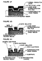
- the substrate 5 is prepared as shown in Figure 2A.
- this substrate 5 is formed of for example, an insulating substrate such as a MgO (100) substrate, a SrTiO3 (100) substrate or others, or a semiconductor substrate such as a silicon (100) substrate having a principal surface coated with insulating films.
- the principal surface of the substrate is continuously coated with MgAl2O4 by the CVD process and with BaTiO3 by the sputtering process.
- a SiO2 layer 15 having a thickness of not less than 200 nanometers is formed on a central portion of the principal surface of the substrate 5 corresponding to a superconducting channel forming position.
- an a -axis orientated oxide superconductor thin film 15 also having a thickness of not less than 200 nanometers is deposited on the principal surface of the substrate 5, by for example an off-axis sputtering.
- the oxide superconductor material is preferably formed of, for example, a Y-Ba-Cu-O type compound oxide superconductor material, a Bi-Sr-Ca-Cu-O type compound oxide superconductor material, and a Tl-Ba-Ca-Cu-O type compound oxide superconductor material.
- a portion 52 of the a-axis orientated oxide superconductor thin film 15 deposited on the SiO2 layer 51 becomes a non-superconductor layer because crystallizability in the portion 52 deposited on the SiO2 layer 51 is disturbed or destroyed.
- the non-superconductor layer 52 and the SiO2 layer 51 are removed by a dry etching process such as the Ar-ion etching, as shown in Figure 2D, so that a superconductor source region (electrode) 12 and a superconductor drain region (electrode) 13 formed of the a-axis oriented oxide superconductor thin film are left or formed because of the etching speed difference due to difference in crystallizability between the a-axis orientated oxide superconductor thin film 15 and the non-superconductor layer 52
- a c -axis oriented oxide superconductor thin film 11 which has a thickness of not greater than five nanometers and which is formed of the same superconductor material as that of the a-axis oriented oxide superconductor thin film 15, is deposited on the principal surface of the substrate 5, the superconductor source region 12 and the superconductor drain region 13, by for example an off-axis sputtering, a reactive evaporation, the MBE, the CVD, etc.
- an insulating layer 16 is deposited on the oxide superconductor thin film 11, and a normal conductor layer 17 for a gate electrode is deposited on the insulating layer 16.
- the insulating layer 16 has a thickness sufficient to prevent a tunnel current, for example, a thickness of not less than 10 nanometers.
- the insulating layer 16 is preferably formed of an insulating material such as Si3N4 or MgO, which does not form a large density of energy levels between the superconductor thin film 11 and the insulating layer 16.
- the normal conductor layer 17 is deposited by any deposition process, for example, the vacuum evaporation, to have a thickness of about 200 nanometer.
- the normal conductor layer 17 is preferably formed of a refractory metal such as Ti, W, etc., or Au, or a silicide thereof. It is preferred that the insulating layer 16 and the normal conductor layer 17 are continuously deposited on the superconductor thin film 11 without being taken out of a deposition chamber, in order to reduce a mechanical stress.
- the insulating layer 16 and the normal conductor layer 17 are selectively etched by the reactive ion etching and the Ar-ion milling so as to form an gate electrode 4 and a gate insulator 6, as shown in Figure 2G.
- the gate insulator 6 is side-etched in comparison with the gate electrode 4 so that the length of the gate insulator 6 is shorter than that of the gate electrode 4.
- the c -axis oriented oxide superconducting thin film 11 on the superconducting source region 12 and the superconductor drain region 13 are removed, and then, a source electrode 2 and a drain electrode 3 formed of the same material as that of the gate electrode 4 are deposited on the superconducting source region 12 and the superconducting drain region 13, respectively, as shown in Figure 2G.
- the super-FET shown in Figure 2H includes the extremely thin c -axis oriented oxide superconductor film 11 formed on the principal surface of the substrate 5, and the superconducting source region 12 and the superconducting drain region 13 formed of the a-axis oriented oxide superconductor thin film.
- the superconducting channel 10 is formed of the extremely thin c -axis oriented oxide superconductor film having the thickness of about five nanometers.
- the superconductor source region 12 and the superconductor drain region 13 are formed of the a-axis oriented oxide superconductor thin film having the thickness of about 200 nanometers.
- the gate electrode 4 is located on the superconducting channel 10 through the gate insulator 6.
- the source electrode 2 and the drain electrode 3 are formed on the superconductor source region 12 and he superconductor drain region 13.
- a main current flows through the superconducting channel and is controlled by the gate voltage. Therefore, differently from the conventional super-FET in which a superconducting current flows through the semiconductor channel due to the superconducting proximity effect, the limitation in the fine processing techniques required for manufacturing the super-FET can be relaxed. In addition, since it is not necessary to stack the superconductor and the semiconductor, high performance superconducting device can be realized by using an oxide superconductor. Therefore, the application of the superconduction technology to the electronic devices can be promoted.
Claims (17)
- Dispositif supraconducteur comprenant un substrat (5) , un canal supraconducteur (10) constitué d'un film mince de supraconducteur d'oxyde formé sur une surface principale plane dudit substrat , d'une électrode de source supraconductrice (2) et d'une électrode de drain supraconductrice (3) formées au niveau des extrémités opposées du canal supraconducteur, de sorte qu'un courant supraconducteur puisse circuler dans ledit canal supraconducteur entre ladite électrode de source supraconductrice et ladite électrode de drain supraconductrice , et d'une électrode de grille (4) placé par l'intermédiaire d'une couche isolante (6) sur le canal supraconducteur de façon à commander le courant supraconducteur circulant dans le canal supraconducteur, ledit film mince de supraconducteur d'oxyde dudit canal supraconducteur (10) étant constitué d'une couche cristalline (1) de supraconducteur d'oxyde orienté selon l'axe c s'étendant sur ladite surface principale dudit substrat et sur une zone isolante en saillie (50) formée sur ladite surface principale, et ledit film mince de supraconducteur d'oxyde de ladite électrode de source supraconductrice (2) et de ladite électrode de drain supraconductrice (3) étant formé d'une couche de film mince de cristal supraconducteur d'oxyde orienté selon l'axe a et étant placé sur ledit film mince (1) de supraconducteur d'oxyde orienté selon l'axe c au niveau des deux côtés de ladite zone isolante en saillie (50), ledit canal supraconducteur étant en continuité avec ladite électrode de source supraconductrice et ladite électrode de drain supraconductrice.
- Dispositif supraconducteur selon la revendication 1 dans lequel ledit film mince de supraconducteur d'oxyde de ladite électrode de source supraconductrice et de ladite électrode de drain supraconductrice est constitué du même matériau que celui dudit film mince de supraconducteur d'oxyde dudit canal supraconducteur.
- Dispositif supraconducteur selon la revendication 1 dans lequel ledit film mince de supraconducteur d'oxyde orienté selon l'axe c est évidé superficiellement au niveau des deux côtés de ladite zone isolante en saillie et ladite électrode de source supraconductrice et ladite électrode de drain supraconductrice sont placées sur les zones superficiellement évidées dudit film mince de supraconducteur d 'oxyde orienté selon l'axe c au niveau des deux côtés de ladite zone isolante formant saillie.
- Dispositif supraconducteur selon la revendication 3 dans lequel lesdites parties superficiellement évidées dudit film mince de supraconducteur d'oxyde orienté selon l'axe c formées au niveau des deux côtés de ladite zone isolante en saillie présentent une épaisseur qui n'est pas inférieure à dix nanomètres.
- Dispositif supraconducteur selon la revendication 1 dans lequel le film mince de supraconducteur d'oxyde est formé d'un matériau sélectionné dans le groupe constitué d'un matériau de supraconducteur d'oxyde composé de type Y-Ba-Cu-O, d'un matériau de supraconducteur d'oxyde composé de type Bi-Sr-Ca-Cu-O et d'un matériau de supraconducteur d'oxyde composé de type Tl-Ba-Ca-Cu-O.
- Dispositif supraconducteur comprenant un substrat (5) , un canal supraconducteur (10) constitué d'un film mince de supraconducteur d'oxyde formé sur une surface principale plane dudit substrat , une zone de source supraconductrice (12) et une zone de drain supraconductrice (13) formées aux extrémités opposées du canal supraconducteur , de sorte qu'un courant supraconducteur peut circuler dans ledit canal supraconducteur entre ladite zone de source supraconductrice et ladite zone de drain supraconductrice, et une électrode de grille (4) placée par l'intermédiaire d'une couche isolante (6) sur le canal supraconducteur de façon à commander le courant supraconducteur circulant dans le canal supraconducteur , ledit film mince de supraconducteur d'oxyde dudit canal supraconducteur étant formé d'une couche cristalline (11) de supraconducteur d'oxyde orienté selon l'axe c et ledit film mince de supraconducteur d'oxyde de ladite zone de source supraconductrice et de ladite zone de drain supraconductrice étant formé d'un cristal de supraconducteur d'oxyde orienté selon l'axe a , ledit canal supraconducteur étant en continuité avec ladite zone de source supraconductrice et ladite zone de drain supraconductrice, dans lequel ladite zone de source supraconductrice et ladite zone de drain supraconductrice sont placées sur ladite surface principale plane dudit substrat à distance l'une de l'autre, et ledit film mince de supraconducteur d ' oxyde orienté selon l'axe c dudit canal supraconducteur est formé sur ladite surface principale plane dudit substrat pour s'étendre sur ladite zone de source supraconductrice et sur ladite zone de drain supraconductrice.
- Dispositif supraconducteur selon la revendication 6 dans lequel ladite électrode de grille (4) est formée d'un matériau conducteur normal placé sur ledit canal supraconducteur et une électrode de source et une électrode de drain constituées d'un matériau conducteur normal sont formées, respectivement, sur ladite zone supraconductrice et ladite zone de drain supraconductrice
- Dispositif supraconducteur selon la revendication 6 dans lequel le film mince de supraconducteur d'oxyde est formé d'un matériau sélectionné dans le groupe constitué d'un matériau supraconducteur d 'oxyde composé de type Y-Ba-Cu-O, d'un matériau supraconducteur d'oxyde composé de type Bi-Sr-Ca-Cu-O et d'un matériau supraconducteur d'oxyde composé de type Tl-Ba-Ca-Cu-O.
- Disposiif supraconducteur selon la revendication 6 dans lequel le substrat est formé d'un matériau sélectionné dans le groupe constitué d'un substrat de MgO (100) , d'un substrat de SrTiO₃ (100) et d'un substrat de CdNdAlO₄ (001) , et d'un substrat semiconducteur.
- Dispositif supraconducteur selon la revendication 6 dans lequel le substrat est formé d'un substrat de silicium et une surface principale du substrat de silicium est recouverte de couches de matériau isolant qui sont constituées d'une couche de MgAl₂O₄ et d'une couche de BaTiO₃.
- Procédé de fabrication d'un dispositif supraconducteur, comprenant les étapes consistant à préparer un substrat (5) comportant une zone isolante en saillie (50) formée sur une surface principale de ce substrat, à former un film mince (1) de supraconducteur d'oxyde orienté selon l'axe c sur la surface principale du substrat incluant la partie en saillie de sorte qu'une épaisseur du film mince de supraconducteur d'oxyde déposé sur ladite zone isolante en saillie est plus mince que celle du film mince de supraconducteur d'oxyde déposé sur le substrat autre que ladite zone isolante en saillie, à fournir une électrode de grille (4) à travers un isolateur de grille (6) sur une partie dudit film mince de supracondcuteur d'oxyde orienté selon l'axe c déposé sur ladite zone isolante en saillie , à évider superficiellement ledit film mince de supraconducteur d'oxyde orienté selon l'axe c au niveau des deux côtés de ladite zone isolante en saillie, et à former une électrode de source supraconductrice (2) et une électrode de drain supraconductrice (3) constituées d'un film mince de supraconducteur d'oxyde orienté selon l'axe a sur les parties évidées superficiellement , dudit film mince de supraconducteur d'oxyde orienté selon l'axe c au niveau des deux côtés de ladite zone isolante en saillie .
- Procédé selon la revendication 11 dans lequel ledit film mince de supraconducteur d 'oxyde orienté selon l'axe c est formé de façon que l'épaisseur du film mince de supraconducteur d'oxyde sur ladite zone isolante en saillie n'est pas supérieure à cinq nanomètres et lesdites parties superficiellement évidées dudit film mince de supraconducteur d'oxyde orienté selon l'axe c sont réalisées en gravant ledit film mince de supraconducteur d'oxyde orienté selon l'axe c au niveau des deux côtés de ladite zone isolante en saillie sur une profondeur qui n'est pas inférieure à dix nanomètres.
- Procédé selon la revendication 11 dans lequel lesdites zones superficiellement évidées dudit film mince de supraconducteur d'oxyde orienté selon l'axe c sont réalisées en formant un masque de métal réfractaire sur ladite électrode de grille et en gravant ledit film mince de supraconducteur d'oxyde orienté selon l'axe c en utilisant ledit masque de métal réfractaire comme masque , et ladite électrode de source supraconductrice et ladite électrode de drain supraconductrice constituées dudit film mince de supraconducteur d'oxyde orienté selon l'axe a sont formées sur les zones superficiellement évidées dudit film mince de supraconducteur d'oxyde orienté selon l'axe c au niveau des deux côtés de ladite zone isolante en saillie en déposant un film mince de supraconducteur d'oxyde orienté selon l'axe a en utilisant ledit masque de métal réfractaire comme un masque.
- Procédé de fabrication d'un dispositif supraconducteur, comprenant les étapes consistant à préparer un substrat (5) présentant une surface principale plane, à former une zone de source supraconductrice (12) et une zone de drain supraconductrice (13) constituées d'un film mince de supraconducteur d'oxyde orienté selon l'axe a sur ladite surface principale planaire dudit substrat à distance l'une de l'autre, à former sur ladite surface principale dudit substrat un film mince (11) de supraconducteur d'oxyde orienté selon l'axe c qui est plus mince que ledit film mince de supraconducteur d'oxyde orienté selon l'axe a, de sorte qu'un canal supraconducteur (10) est formé entre ladite zone de source supraconductrice et ladite zone de drain supraconductrice, à fournir une électrode de grille (4) à travers un isolateur de grille (6) sur ledit film mince de supraconducteur d'oxyde orienté selon l'axe c entre ladite zone de source supraconductrice et ladite zone de drain supraconductrice, à éliminer une partie dudit film mince de supraconducteur d'oxyde orienté selon l'axe c sur chacune desdites zones de source supraconductrice et de drain supraconductrice , et à constituer une électrode de source (2) et une électrode de drain (3) d'un matériau conducteur normal sur une partie exposée de ladite zone de source supraconductrice et de ladite zone de drain supraconductrice, respectivement.
- Procédé selon la revendication 14 dans lequel ladite zone de source supraconductrice (12) et ladite zone de drain supraconductrice (13) sont formées en déposant une couche perturbant le cristal sur un endroit sélectionné de ladite surface principale dudit substrat , à déposer de façon uniforme un film mince de supraconducteur d'oxyde orienté selon l'axe a sur ladite surface principale dudit substrat de façon à recouvrir ladite couche perturbant le cristal, de sorte qu'une partie du film mince de supraconducteur d'oxyde orienté selon l'axe a déposé sur ladite couche perturbant le cristal devient non supraconductrice , et à éliminer sélectivement une zone non supraconductrice dudit film mince de supraconducteur d'oxyde orienté selon l'axe a déposé sur ladite couche perturbant le cristal et ladite couche perturbant le cristal , de façon que deux parties du film mince de supraconducteur d'oxyde orienté selon l'axe a soient formées à distance l'une de l'autre afin de réaliser ladite zone de source supraconductrice et ladite zone de drain supraconductrice.
- Procédé selon la revendication 15 dans lequel ladite couche perturbant le cristal est constituée de SiO₂.
- Procédé selon la revendication 16 dans lequel ladite partie non supraconductrice dudit film mince de supraconducteur d 'oxyde orienté selon l'axe a déposé sur ladite couche de SiO₂ et ladite couche de SiO₂ sont sélectivement éliminées par un procédé de gravure sèche en utilisant la différence de vitesse de gravure due à la différence d'aptitude à cristalliser entre ledit film mince de supraconducteur d'oxyde orienté selon l'axe a et ladite partie non supraconductrice.
Applications Claiming Priority (4)
| Application Number | Priority Date | Filing Date | Title |
|---|---|---|---|
| JP2270070A JP2641975B2 (ja) | 1990-10-08 | 1990-10-08 | 超電導素子および作製方法 |
| JP270070/90 | 1990-10-08 | ||
| JP2287830A JP2641976B2 (ja) | 1990-10-25 | 1990-10-25 | 超電導素子および作製方法 |
| JP287830/90 | 1990-10-25 |
Publications (3)
| Publication Number | Publication Date |
|---|---|
| EP0480814A2 EP0480814A2 (fr) | 1992-04-15 |
| EP0480814A3 EP0480814A3 (en) | 1992-08-05 |
| EP0480814B1 true EP0480814B1 (fr) | 1996-04-24 |
Family
ID=26549051
Family Applications (1)
| Application Number | Title | Priority Date | Filing Date |
|---|---|---|---|
| EP91402677A Expired - Lifetime EP0480814B1 (fr) | 1990-10-08 | 1991-10-08 | Dispositif supraconducteur avec un canal ultra-mince forme en matériau supraconducteur d'oxyde et procédé pour sa fabrication |
Country Status (4)
| Country | Link |
|---|---|
| US (2) | US5236896A (fr) |
| EP (1) | EP0480814B1 (fr) |
| CA (1) | CA2052970C (fr) |
| DE (1) | DE69119022T2 (fr) |
Families Citing this family (31)
| Publication number | Priority date | Publication date | Assignee | Title |
|---|---|---|---|---|
| CA2051778C (fr) * | 1990-09-19 | 1997-05-06 | Takao Nakamura | Methode de fabrication d'un dispositif supraconducteur a couche d'oxyde supraconducteur d'epaisseur reduite, et dispositif supraconducteur ainsi fabrique |
| DE69115209T2 (de) * | 1990-09-28 | 1996-08-08 | Sumitomo Electric Industries | Verfahren zur Herstellung eines Supraleitungsbauelements mit reduzierter Dicke der supraleitenden Oxidschicht und dadurch hergestelltes Supraleitungsbauelement. |
| DE69124072T2 (de) * | 1990-10-31 | 1997-08-07 | Sumitomo Electric Industries | Supraleitende Schaltung und Verfahren zu ihrer Herstellung |
| CA2054795C (fr) * | 1990-11-01 | 1996-08-06 | Hiroshi Inada | Dispositif a canal fait d'une couche d'oxyde supraconducteur extremement mince et sa methode de fabrication |
| US5134117A (en) * | 1991-01-22 | 1992-07-28 | Biomagnetic Technologies, Inc. | High tc microbridge superconductor device utilizing stepped edge-to-edge sns junction |
| EP0591312B1 (fr) * | 1991-06-24 | 1997-08-06 | Forschungszentrum Jülich Gmbh | Pistes conductrices structurees et leur procede de fabrication |
| EP0534854B1 (fr) * | 1991-09-24 | 1997-12-03 | Sumitomo Electric Industries, Ltd. | Couche mince supraconducteur de matériau supraconducteur en oxyde, trajet supraconducteur du courant et dispositif supraconducteur utilisant la couche mince supraconducteur |
| JP2773487B2 (ja) * | 1991-10-15 | 1998-07-09 | 日本電気株式会社 | トンネルトランジスタ |
| WO1993010565A1 (fr) * | 1991-11-13 | 1993-05-27 | Seiko Epson Corporation | Element supraconducteur |
| CA2084174C (fr) * | 1991-11-30 | 1997-07-29 | Takao Nakamura | Dispositif a superconduction comportant un canal superconducteur tres mince compose d'un materiau superconducteur oxyde et methode de fabrication |
| DE69218388T2 (de) * | 1991-12-10 | 1997-10-23 | Sumitomo Electric Industries | Supraleitendes Bauelement mit extrem dünnem Kanal aus supraleitendem Oxyd und sein Herstellungsverfahren |
| CA2085172C (fr) * | 1991-12-12 | 1996-07-23 | Takao Nakamura | Dispositif supraconducteur a canal d'oxyde supraconducteur extremement mince et methode de fabrication de ce dispositif |
| JPH05251776A (ja) * | 1991-12-13 | 1993-09-28 | Sumitomo Electric Ind Ltd | 超電導素子およびその作製方法 |
| US5552374A (en) * | 1992-04-09 | 1996-09-03 | Sumitomo Electric Industries, Ltd. | Oxide superconducting a transistor in crank-shaped configuration |
| JP2822773B2 (ja) * | 1992-04-28 | 1998-11-11 | 住友電気工業株式会社 | 超電導インタフェース回路 |
| CA2099640A1 (fr) * | 1992-06-24 | 1993-12-25 | Michitomo Iiyama | Dispositif supraconducteur ayant une voie supraconductrice formee d'oxyde supraconducteur et methode de fabrication connexe |
| US5828079A (en) * | 1992-06-29 | 1998-10-27 | Matsushita Electric Industrial Co., Ltd. | Field-effect type superconducting device including bi-base oxide compound containing copper |
| EP1544926A3 (fr) * | 1992-07-28 | 2005-07-20 | Nippon Telegraph And Telephone Corporation | Dispositif supraconducteur à couches minces comprenant des interconnexions à multicouches en oxide supraconducteur et son procédé de fabrication |
| JPH0745880A (ja) * | 1993-07-29 | 1995-02-14 | Sumitomo Electric Ind Ltd | 絶縁体薄膜と酸化物超電導薄膜との積層膜 |
| KR0148596B1 (ko) * | 1994-11-28 | 1998-10-15 | 양승택 | 결정 입계 채널을 갖는 초전도 전계효과 소자와 그 제조방법 |
| JPH08227743A (ja) * | 1995-02-20 | 1996-09-03 | Sumitomo Electric Ind Ltd | 酸化物超電導体用金属電極 |
| KR100194621B1 (ko) * | 1995-12-21 | 1999-07-01 | 정선종 | 고온초전도 전계효과 소자 및 그 제조방법 |
| US5994276A (en) | 1997-09-08 | 1999-11-30 | Mcmaster University | Composite high Tc superconductor film |
| US6660598B2 (en) * | 2002-02-26 | 2003-12-09 | International Business Machines Corporation | Method of forming a fully-depleted SOI ( silicon-on-insulator) MOSFET having a thinned channel region |
| JP2005056754A (ja) * | 2003-08-06 | 2005-03-03 | Sumitomo Electric Ind Ltd | 超電導線材およびその製造方法 |
| US7553704B2 (en) * | 2005-06-28 | 2009-06-30 | Freescale Semiconductor, Inc. | Antifuse element and method of manufacture |
| US20070254402A1 (en) * | 2006-04-27 | 2007-11-01 | Robert Rotzoll | Structure and fabrication of self-aligned high-performance organic fets |
| US9993364B2 (en) | 2013-09-26 | 2018-06-12 | 3 West C, Llc | Ostomy bag |
| US10238529B2 (en) | 2013-09-26 | 2019-03-26 | 3 West C. LLC | Ostomy bag |
| US11298257B2 (en) | 2017-03-22 | 2022-04-12 | 3 West C, Llc. | Ostomy apparatuses and related methods |
| DE102020112143B4 (de) | 2020-05-05 | 2022-03-17 | Lts Lohmann Therapie-Systeme Ag | Nicotin - Corona |
Citations (1)
| Publication number | Priority date | Publication date | Assignee | Title |
|---|---|---|---|---|
| EP0478465A1 (fr) * | 1990-09-28 | 1992-04-01 | Sumitomo Electric Industries, Ltd. | Procédé de fabrication d'un dispositif supraconducteur ayant une couche d'oxyde supraconductrice à épaisseur réduite et dispositif à supraconducteur fabriqué ainsi |
Family Cites Families (10)
| Publication number | Priority date | Publication date | Assignee | Title |
|---|---|---|---|---|
| US4751563A (en) * | 1984-11-05 | 1988-06-14 | International Business Machines, Corp. | Microminiaturized electrical interconnection device and its method of fabrication |
| EP0276746B1 (fr) * | 1987-01-30 | 1994-07-13 | Hitachi, Ltd. | Dispositif supraconducteur |
| KR910002311B1 (ko) * | 1987-02-27 | 1991-04-11 | 가부시기가이샤 히다찌세이사꾸쇼 | 초전도 디바이스 |
| US5212150A (en) * | 1987-05-06 | 1993-05-18 | Semiconductor Energy Laboratory Co., Ltd. | Oxide superconducting lead for interconnecting device component with a semiconductor substrate via at least one buffer layer |
| US5183800A (en) * | 1987-07-15 | 1993-02-02 | Sharp Kabushiki Kaisha | Interconnection method for semiconductor device comprising a high-temperature superconductive material |
| EP0324044B1 (fr) * | 1988-01-15 | 1992-11-25 | International Business Machines Corporation | Dispositif à effet de champ à canal supraconducteur |
| US4878094A (en) * | 1988-03-30 | 1989-10-31 | Minko Balkanski | Self-powered electronic component and manufacturing method therefor |
| JP2862137B2 (ja) * | 1988-08-11 | 1999-02-24 | 古河電気工業株式会社 | 超電導トランジスタ |
| US5135908A (en) * | 1989-08-07 | 1992-08-04 | The Trustees Of Columbia University In The City Of New York | Method of patterning superconducting films |
| JP2913785B2 (ja) * | 1990-07-12 | 1999-06-28 | 富士通株式会社 | 半導体装置の製造方法 |
-
1991
- 1991-10-08 EP EP91402677A patent/EP0480814B1/fr not_active Expired - Lifetime
- 1991-10-08 DE DE69119022T patent/DE69119022T2/de not_active Expired - Fee Related
- 1991-10-08 US US07/771,986 patent/US5236896A/en not_active Expired - Fee Related
- 1991-10-08 CA CA002052970A patent/CA2052970C/fr not_active Expired - Fee Related
-
1993
- 1993-04-28 US US08/053,401 patent/US5322526A/en not_active Expired - Fee Related
Patent Citations (1)
| Publication number | Priority date | Publication date | Assignee | Title |
|---|---|---|---|---|
| EP0478465A1 (fr) * | 1990-09-28 | 1992-04-01 | Sumitomo Electric Industries, Ltd. | Procédé de fabrication d'un dispositif supraconducteur ayant une couche d'oxyde supraconductrice à épaisseur réduite et dispositif à supraconducteur fabriqué ainsi |
Also Published As
| Publication number | Publication date |
|---|---|
| EP0480814A2 (fr) | 1992-04-15 |
| CA2052970C (fr) | 1996-07-02 |
| US5236896A (en) | 1993-08-17 |
| DE69119022T2 (de) | 1996-10-31 |
| DE69119022D1 (de) | 1996-05-30 |
| EP0480814A3 (en) | 1992-08-05 |
| CA2052970A1 (fr) | 1992-04-09 |
| US5322526A (en) | 1994-06-21 |
Similar Documents
| Publication | Publication Date | Title |
|---|---|---|
| EP0480814B1 (fr) | Dispositif supraconducteur avec un canal ultra-mince forme en matériau supraconducteur d'oxyde et procédé pour sa fabrication | |
| US5407903A (en) | Superconducting device having a reduced thickness of oxide superconducting layer | |
| US5416072A (en) | Superconducting device having an thin superconducting channel formed of oxide superconducting material | |
| US5717222A (en) | Superconducting device having an extremely thin superconducting channel formed of oxide superconductor material and method for manufacturing the same | |
| US5547923A (en) | Method for manufacturing superconducting device having a reduced thickness of oxide superconducting layer | |
| EP0475838B1 (fr) | Dispositif supraconducteur avec un film supraconducteur de épaisseur réduite et methode pour sa fabrication | |
| EP0484232B2 (fr) | Dispositif supraconducteur ayant un canal supraconducteur extrêmement court en matériau supraconducteur d'oxyde et méthode pour sa fabrication | |
| EP0477063B1 (fr) | Dispositif à supraconducteur ayant une couche d'oxyde supraconductrice à épaisseur réduite et procédé pour sa fabrication | |
| US5714767A (en) | Method for manufacturing superconducting device having a reduced thickness of oxide superconducting layer and superconducting device manufactured thereby | |
| US5447907A (en) | Superconducting device with c-axis channel and a-axis source and drain having a continuous crystal structure | |
| EP0533519B1 (fr) | Dispositif supraconducteur ayant un canal extrêmement mince, formé en matériau supraconducteur d'oxyde et méthode pour sa fabrication | |
| EP0478463B1 (fr) | Dispositif à supraconducteur avec un canal supraconducteur extrêmement mince formé d'un matériau d'oxyde supraconducteur | |
| CA2186840C (fr) | Dispositif a effet de champ a canal supraconducteur et methode de fabrication de ce dispositif | |
| JP2641966B2 (ja) | 超電導素子および作製方法 | |
| JP2641976B2 (ja) | 超電導素子および作製方法 | |
| CA2243654A1 (fr) | Dispositif supraconducteur a effet de champ comportant un canal supraconducteur et methode de fabrication de ce dispositif |
Legal Events
| Date | Code | Title | Description |
|---|---|---|---|
| PUAI | Public reference made under article 153(3) epc to a published international application that has entered the european phase |
Free format text: ORIGINAL CODE: 0009012 |
|
| AK | Designated contracting states |
Kind code of ref document: A2 Designated state(s): DE FR GB |
|
| PUAL | Search report despatched |
Free format text: ORIGINAL CODE: 0009013 |
|
| AK | Designated contracting states |
Kind code of ref document: A3 Designated state(s): DE FR GB |
|
| 17P | Request for examination filed |
Effective date: 19920811 |
|
| 17Q | First examination report despatched |
Effective date: 19940708 |
|
| GRAA | (expected) grant |
Free format text: ORIGINAL CODE: 0009210 |
|
| AK | Designated contracting states |
Kind code of ref document: B1 Designated state(s): DE FR GB |
|
| REF | Corresponds to: |
Ref document number: 69119022 Country of ref document: DE Date of ref document: 19960530 |
|
| ET | Fr: translation filed | ||
| PLBE | No opposition filed within time limit |
Free format text: ORIGINAL CODE: 0009261 |
|
| STAA | Information on the status of an ep patent application or granted ep patent |
Free format text: STATUS: NO OPPOSITION FILED WITHIN TIME LIMIT |
|
| 26N | No opposition filed | ||
| PGFP | Annual fee paid to national office [announced via postgrant information from national office to epo] |
Ref country code: GB Payment date: 19981009 Year of fee payment: 8 Ref country code: FR Payment date: 19981009 Year of fee payment: 8 |
|
| PGFP | Annual fee paid to national office [announced via postgrant information from national office to epo] |
Ref country code: DE Payment date: 19981016 Year of fee payment: 8 |
|
| PG25 | Lapsed in a contracting state [announced via postgrant information from national office to epo] |
Ref country code: GB Free format text: LAPSE BECAUSE OF NON-PAYMENT OF DUE FEES Effective date: 19991008 |
|
| GBPC | Gb: european patent ceased through non-payment of renewal fee |
Effective date: 19991008 |
|
| PG25 | Lapsed in a contracting state [announced via postgrant information from national office to epo] |
Ref country code: FR Free format text: LAPSE BECAUSE OF NON-PAYMENT OF DUE FEES Effective date: 20000630 |
|
| PG25 | Lapsed in a contracting state [announced via postgrant information from national office to epo] |
Ref country code: DE Free format text: LAPSE BECAUSE OF NON-PAYMENT OF DUE FEES Effective date: 20000801 |
|
| REG | Reference to a national code |
Ref country code: FR Ref legal event code: ST |