EP0476871A1 - Prozessüberwachungsschaltung und Methode dazu - Google Patents
Prozessüberwachungsschaltung und Methode dazu Download PDFInfo
- Publication number
- EP0476871A1 EP0476871A1 EP91307954A EP91307954A EP0476871A1 EP 0476871 A1 EP0476871 A1 EP 0476871A1 EP 91307954 A EP91307954 A EP 91307954A EP 91307954 A EP91307954 A EP 91307954A EP 0476871 A1 EP0476871 A1 EP 0476871A1
- Authority
- EP
- European Patent Office
- Prior art keywords
- delay
- state transition
- logic state
- logic
- input
- Prior art date
- Legal status (The legal status is an assumption and is not a legal conclusion. Google has not performed a legal analysis and makes no representation as to the accuracy of the status listed.)
- Granted
Links
Images


Classifications
-
- H—ELECTRICITY
- H10—SEMICONDUCTOR DEVICES; ELECTRIC SOLID-STATE DEVICES NOT OTHERWISE PROVIDED FOR
- H10P—GENERIC PROCESSES OR APPARATUS FOR THE MANUFACTURE OR TREATMENT OF DEVICES COVERED BY CLASS H10
- H10P74/00—Testing or measuring during manufacture or treatment of wafers, substrates or devices
-
- H—ELECTRICITY
- H10—SEMICONDUCTOR DEVICES; ELECTRIC SOLID-STATE DEVICES NOT OTHERWISE PROVIDED FOR
- H10P—GENERIC PROCESSES OR APPARATUS FOR THE MANUFACTURE OR TREATMENT OF DEVICES COVERED BY CLASS H10
- H10P74/00—Testing or measuring during manufacture or treatment of wafers, substrates or devices
- H10P74/27—Structural arrangements therefor
- H10P74/277—Circuits for electrically characterising or monitoring manufacturing processes, e.g. circuits in tested chips or circuits in testing wafers
Definitions
- This invention relates to a process monitor circuit, in particular in integrated circuit (IC) fabrication and for monitoring PMOS and NMOS transistors in a CMOS process, and to a process monitoring method.
- IC integrated circuit
- a semiconductor die on a wafer often includes not only the product to be manufactured, but also a number of process monitor circuits which are fabricated on the die at the same time.
- the process monitor circuits are tested and their performance serves as a parametric test of the integrity of the manufacturing process.
- a process monitor circuit connected to the input and output pins of the integrated circuit on the die is particularly convenient because the pins are readily accessible by the test equipment. Having the process monitor circuit connected to the input and output pins of the integrated circuit on the die also allows the circuit to be tested at various steps of the manufacturing process, such as wafer sort, final test, at the end user, or wherever correlation of reliability data with process parameters is valuable.
- a long path means any signal path in which the time delay of the path primarily results from the propagation delay of the internal logic circuits, and the time delay is only negligibly contributed to by external factors, such as output capacitive load, or the rise and fall times of the input signals.
- a test structure including a long delay circuit is specially built for the purpose of testing, and included in the circuit to be fabricated.
- This long delay circuit often takes the form of a chain of serially connected inverters. Typically, such a chain may contain 50-5100 inverters.
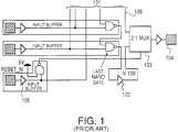
- FIG. 1 shows a process monitor circuit of the prior art including a chain of inverters.
- the process monitor circuit includes a test structure 101, called a NAND tree, for measuring input buffer voltage thresholds of logic states (VIH and VIL).
- the NAND tree 101 is a chain of two-input NAND gates, with each NAND gate's two input terminals connected respectively to the output terminal of an input buffer, and the output terminal of the previous NAND gate in the chain.
- the first NAND gate of the chain has one input terminal connected to the power supply, and the other input terminal connected to the first input buffer of the NAND tree 101.
- the NAND tree 101 allows testing of each input buffer by applying a voltage at the input associated with each input buffer, and examining the output voltage at the output terminal of the last NAND gate in the NAND tree 101.
- the output terminal of the last NAND gate in the NAND tree 101 is connected to the delay logic path 102, similar to the delay circuit discussed above, consisting of 100 serially connected inverters.
- the output of the delay logic path 102 is provided through 2:1 multiplexor 103 at an output pad 104.
- input buffer threshold voltages and the circuit speed attained are measured, respectively, by examining the voltage and the delays of signal transitions at output pad 104. Both tests may be conducted using the same input and output pins because the threshold voltage (VIH and VIL) measurements are not sensitive to circuit speed, which is measured by the propagation delay through delay logic path 102.
- each input pin of the die is dual-purpose, i.e. used as an input pin during testing, and also used as an input or output pin during normal operation.
- the output pin such as output pin 104, is also dual-purpose, serving as an output pin during testing and as an output pin during normal operation.
- the performance of the integrated circuit depends on the performance of both PMOS and NMOS transistors. Since the PMOS and NMOS transistors are formed at different stages of the manufacturing process, variations in process factor at a given step may not affect the PMOS and NMOS transistors equally. As will be explained in the detailed description of the present invention, the performance of the delay logic path 102 does not provide information indicative of the different impacts of process factors on PMOS and NMOS transistors.
- a process monitor circuit in accordance with the present invention, includes a first delay path providing a first delay in response to logic high to logic low logic state transition signal at the input terminal of this first delay path, and providing a second delay when a logic low to logic high logic state transition signal is provided at the same input terminal.
- the process monitor circuit also includes a second delay path providing substantially equal delays for either logic state transition at the same input terminal. The difference between the delays of the first and second delay path for each logic state transition is indicative of the relative performance of the PMOS and NMOS transistors being monitored.
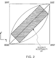
- Figure 2 shows a conceptual diagram of circuit performance, with respect to four process "corners". Circuit performance may be measured by a number of parameters ("figures of merit"), for example, propagation delay with respect to a rising input signal.
- the increasing y direction represents the direction of change in circuit performance due to the variation in the process producing "stronger” NMOS transistor
- the increasing x direction represents the direction of change in circuit performance due to variation in the fabrication process producing "stronger” PMOS transistors.
- a stronger transistor may be defined as, for example, one with higher switching speed.
- the corner labelled "SNSP" represents the conceptual limit of circuit performance when the process is producing both strong NMOS and PMOS transistors.
- NWP represents, respectively, conceptual limits of circuit performance when both PMOS and NMOS transistors are weak, the NMOS transistor is strong while the PMOS transistor is weak, or the NMOS transistor is weak while the PMOS transistor is strong.
- the various objectives of a manufacturing process are optimized when the circuit performance lies between these limits, such as within the shaded rectangle 201, called the "region of acceptability.”
- quality control may be accomplished by a parametric test designed to reject any circuit having a measured performance which lies outside of the region of acceptability.
- the propagation delay in a chain of inverters is not sensitive to the relative strengths of the PMOS and NMOS transistors (i.e. since many combinations of PMOS transistor and NMOS transistor strengths can produce the same propagation delay)
- the propagation delay of a chain of inverters measures the "overall process factor", but is insufficient to determine, for example, if a circuit lies outside the region of acceptability because of a large discrepancy between the strengths of the PMOS and NMOS transistors.
- the parametric test must include a measurement sensitive to the relative strengths of the PMOS and NMOS transistors.
- the present invention takes advantage of the inherent higher speed of the NMOS transistor over the PMOS transistor of the same size. This speed difference is attributed to the higher mobility of electrons (the charge carriers in an NMOS transistor) over holes (the charge carriers in a PMOS transistor). This effect may be seen, for example, in a CMOS NOR gate. In such a NOR gate, a rising edge state transition is always slower than the same state transition in either a CMOS NAND gate or a CMOS inverter. This is because the NOR gate is typically formed by two or more PMOS transistors connected in series in the pull-up stage and an equal number of NMOS transistors connected in parallel to form the pull-down stage.
- the delay of the NOR gate in a rising edge transition is substantially the sum of the delays in the individual PMOS transistors. Furthermore, the delay of the NOR gate in a falling edge transition is substantially the delay of an NMOS transistor divided by the number of NMOS transistors, causing a large difference in delay between rising edge and falling edge transitions ("asymmetric transition property").
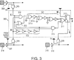
- Figure 3 shows the preferred embodiment of the present invention including test circuit 300.
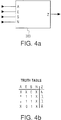
- Figure 4a is block diagram representation of test circuit 300 and Figure 4b is the truth table relating the input signals A, E, S and N of test circuit 300 to its output signal Z.
- the inverted output signal S of input buffer 310 i.e. output signal of NAND gate 309, selects whether test mode output signal at XNOR gate 311 or the output signal N of the functional integrated circuit is selected in the multiplexor 312 to generate output signal Z.
- the inverted output of input buffer 305 i.e. output signal of NAND gate 305, provides an enable signal E, which when ANDed at AND gate 304 with the test mode signal A enables a delay path 301.
- Delay path 301 comprises a chain of OR gates, each of which is made up of a three-input NOR gate, such as NOR gate 301a, and an inverter, such as inverter 301b. Although only three OR gates are shown, the actual number of OR gates is much larger. The exact number of OR gates is not critical, but 50-100 OR gates will provide an appreciable delay difference between this delay path 301 and the second delay path 302 discussed below. In this embodiment, NOR gate 301a has the asymmetric transition property discussed above.
- Inverter 301b is designed such that the delays of its falling edge and rising edge transitions are roughly equal, so that, as a whole, the OR gate formed by NOR gate 301a and inverter 301b preserves the asymmetric transition property of the NOR gate 301a.
- the equal delays in the inverter 301b are accomplished by sizing the pull-up PMOS transistor twice as large as the pull-down NMOS transistor, taking into account the switching speed of an NMOS transistor is roughly twice that of a PMOS transistor of the same size.
- four PMOS transistors and two NMOS transistors, all of equal size, form respectively the pull-up and pull-down stages of each inverter.
- each OR gate of the delay path 301 As a signal is propagated through this delay path 301, the transition in each OR gate of the delay path 301 is of the same polarity, so that the asymmetric transition property of each NOR gate is magnified by the number of NOR gates in the delay path 301.
- the output signal of delay path 301 is provided as an input signal to XNOR (exclusive NOR) gate 311. It will of course be appreciated that the use of XNOR gate 311 is a matter of design choice, and the use of an XOR (exclusive-OR) gate is equally acceptable in practicing the present invention.
- a second delay path 302 comprising a number of inverters serially connected in a chain, is utilized. Unlike the inverters in delay path 301, these inverters are not required to have substantially symmetrical rising and falling edge transitions. Also, although only four inverters are shown in Figure 3, many more are implemented to provide an appreciable delay between the input transition at pin 314 and the output of the delay path 314.
- the propagation delay through the delay path 302 due to a rising edge transition is roughly equal to the propagation delay through the delay path 302 due to a falling edge transition.
- the output signal of the inverter chain 302 is provided as an input to AND gate 302 and NOR gate 303.
- NAND gate 313 allows the output signal of inverter chain 302 to propagate as input to XNOR gate 311.
- the enable signal E is at logic low, the output signal of inverter chain 302 propagates through NOR gate 303 and through the delay path 301.
- the delay paths 301 and 302 together form a long delay path, which is logically an inverter in the implementation shown in Figure 3. (See Figure 4b).
- This delay path is an inverter only because of the even number of inverters implemented in this embodiment. Neither an even number nor an odd number of inverters is necessary to practice the present invention.
- the timing diagram in Figure 5a shows, in the waveform labelled "pin 314", a rising edge transition 501 at the input pin 314 associated with the input buffer 307 (i.e. falling edge transition of signal A), followed by a falling edge transition 502 at the input pin 314.
- the transitions 503 and 504 of output signal Z, in the waveform labelled "Z", due to the transitions 501 and 502 of the input signal at the input pin 314, are respectively delayed by delay periods SDr and SDf as indicated in Figure 5a.
- SDr is the delay between the rising edge transition 501 at input pin 314 and the output signal Z's transition 503.
- SDf is the delay between the falling edge transition 502 at the input pin 314 and the output signal Z's transition 504.
- the average of these delays ((SDr+SDf)/2) provides an indication of the overall process factor.
- the delay paths 301 and 302 form two parallel delay paths with the respective output signal of each delay path provided as inputs to XNOR gate 311.
- the number of the OR gates in delay path 301 is much larger than the number of inverters in delay path 302, which ensures that the logic transition of output signal Z due to output transitions in the delay path 301 will always arrive later than the logic transition of output signal Z due to the output transitions in delay path 302.
- the ratio of the number of OR gates (in path 301) to the number of inverters (in path 302) be as illustrated in Figure 3.
- either a rising edge transition or a falling edge transition will cause a pulse of the same polarity at the output signal Z.
- the rising edge of each pulse represents the transition propagated through the delay path 302, which is the shorter delay path.
- the falling edge of each pulse is the transition propagated through the longer delay path 301.
- Figure 5b shows a rising edge transitions 521 and a falling edge transition 522 of the input signal at the input pin 314.
- pulses 520a and 520b are produced.
- rising edge 523 of pulse 520a having a delay IVr
- the falling edge 524 of pulse 520a having a delay ORr
- the falling edge transition 526, having a delay ORf correspond respectively to the transitions propagated through delay paths 302 and 301.
- IVr is the delay between rising edge transition 521 at the input pin 314 and the transition 523 output signal Z, corresponding to propagation in the delay path 302.
- ORr is the delay between rising edge transition 521 at the input pin 314 and the transition 524 of output signal Z, corresponding to signal propagation in the delay path 301.
- IVf is the delay between falling edge transition 522 at the input pin 314 and the transition 525 of output signal Z, corresponding to signal propagation in the delay path 302.
- ORf is the delay between falling edge transition 522 at the input pin 314 and the transition 526 of the output signal Z, corresponding to signal propagation in the delay path 301.
- the pulses 520a and 520b are not of the same duration. Specifically, a stronger PMOS transistor will shorten the pulse 520a, and a stronger NMOS transistor will shorten pulse 520b.
- the ratio ((ORr-IVr)/(IVf-ORf)) provides a parameter to measure the relative strengths of the PMOS and NMOS transistors.
- the quantity (IVf-ORf) may be very small, e.g. as small as 4ns
- the ratio ((ORr-IVr)/IVr) is another parameter suitable for measuring the relative strengths of the PMOS and NMOS transistors.
- Figure 6 is a table of results from a simulation of the circuit shown in Figure 3, under the seven process conditions: weak N - weak P (WNWP), and nominal N - nominal P (NNNP), strong N - strong P (SNSP), weak N - strong P (WNSP), strong N - weak P (SNWP), nominal N - weak P (NNWP) and weak N - nominal P (WNNP).
- the first PULSEWIDT field corresponds to the pulse width A of pulse 520a, in response to the logic low to logic high transition at the input pin 314.
- the second PULSEWIDT field correspond to the pulse width B of pulse 520b, in response to logic high to logic low transition at input pin 314.
- the value D is the delay time between the input transition at input pin 314 and the rising edge of pulse 520a.
- This value D is used to compute a correction Factor CF, which is used to compute a normalized parameter "NORMALIZED" of the pulse widths of pulses 520a and 520b.
- A+2D is the pulse width A plus two times the delay D; this sum roughly corresponds to the sum of delay paths 301 and 302. 166.556 is the total delay of these delay paths under process condition NNNP, while 4.405 is the ratio of A/B under the same NNNP process condition.
- the value 532.5 is chosen to minimize the magnitudes of NORMALIZED under WNWF and SNSP conditions.
- the value of the parameter NORMALIZED represents the relative strengths of the PMOS and NMOS transistors under the actual process condition.
Landscapes
- Tests Of Electronic Circuits (AREA)
- Testing Of Individual Semiconductor Devices (AREA)
- Testing Or Measuring Of Semiconductors Or The Like (AREA)
- Semiconductor Integrated Circuits (AREA)
Applications Claiming Priority (2)
| Application Number | Priority Date | Filing Date | Title |
|---|---|---|---|
| US577945 | 1990-09-05 | ||
| US07/577,945 US5068547A (en) | 1990-09-05 | 1990-09-05 | Process monitor circuit |
Publications (2)
| Publication Number | Publication Date |
|---|---|
| EP0476871A1 true EP0476871A1 (de) | 1992-03-25 |
| EP0476871B1 EP0476871B1 (de) | 1997-04-16 |
Family
ID=24310785
Family Applications (1)
| Application Number | Title | Priority Date | Filing Date |
|---|---|---|---|
| EP91307954A Expired - Lifetime EP0476871B1 (de) | 1990-09-05 | 1991-08-30 | Prozessüberwachungsschaltung und Methode dazu |
Country Status (5)
| Country | Link |
|---|---|
| US (1) | US5068547A (de) |
| EP (1) | EP0476871B1 (de) |
| JP (1) | JP3137269B2 (de) |
| KR (1) | KR100237504B1 (de) |
| DE (1) | DE69125672T2 (de) |
Cited By (1)
| Publication number | Priority date | Publication date | Assignee | Title |
|---|---|---|---|---|
| EP0755119A1 (de) * | 1995-07-20 | 1997-01-22 | Matra Mhs | Verfahren zur Analog-Digital-Wandlung |
Families Citing this family (34)
| Publication number | Priority date | Publication date | Assignee | Title |
|---|---|---|---|---|
| US5486786A (en) * | 1994-08-09 | 1996-01-23 | Lsi Logic Corporation | Process monitor for CMOS integrated circuits |
| US5631596A (en) * | 1994-08-09 | 1997-05-20 | Lsi Logic Corporation | Process monitor for CMOS integrated circuits |
| DE19528733C1 (de) * | 1995-08-04 | 1997-01-02 | Siemens Ag | Integrierte Schaltung |
| US6005406A (en) * | 1995-12-07 | 1999-12-21 | International Business Machines Corporation | Test device and method facilitating aggressive circuit design |
| US5872449A (en) * | 1996-01-26 | 1999-02-16 | Lsi Logic Corporation | Semiconductor package qualification chip |
| US5796265A (en) * | 1996-02-29 | 1998-08-18 | Lsi Logic Corporation | Method for metal delay testing in semiconductor devices |
| US5796260A (en) * | 1996-03-12 | 1998-08-18 | Honeywell Inc. | Parametric test circuit |
| US5654895A (en) * | 1996-04-04 | 1997-08-05 | Lsi Logic Corporation | Process monitor usig impedance controlled I/O controller |
| US5751161A (en) * | 1996-04-04 | 1998-05-12 | Lsi Logic Corporation | Update scheme for impedance controlled I/O buffers |
| US5867033A (en) * | 1996-05-24 | 1999-02-02 | Lsi Logic Corporation | Circuit for testing the operation of a semiconductor device |
| US6097884A (en) * | 1997-12-08 | 2000-08-01 | Lsi Logic Corporation | Probe points and markers for critical paths and integrated circuits |
| US6124143A (en) * | 1998-01-26 | 2000-09-26 | Lsi Logic Corporation | Process monitor circuitry for integrated circuits |
| US6061814A (en) * | 1998-04-21 | 2000-05-09 | Lsi Logic Corporation | Test circuitry for determining the defect density of a semiconductor process as a function of individual metal layers |
| US6185706B1 (en) | 1998-06-12 | 2001-02-06 | Lsi Logic Corporation | Performance monitoring circuitry for integrated circuits |
| US6367042B1 (en) | 1998-12-11 | 2002-04-02 | Lsi Logic Corporation | Testing methodology for embedded memories using built-in self repair and identification circuitry |
| US6067262A (en) * | 1998-12-11 | 2000-05-23 | Lsi Logic Corporation | Redundancy analysis for embedded memories with built-in self test and built-in self repair |
| US6651202B1 (en) | 1999-01-26 | 2003-11-18 | Lsi Logic Corporation | Built-in self repair circuitry utilizing permanent record of defects |
| US6389578B1 (en) * | 1999-05-26 | 2002-05-14 | Hewlett-Packard Company | Method and apparatus for determining the strengths and weaknesses of paths in an integrated circuit |
| US6449749B1 (en) * | 1999-11-18 | 2002-09-10 | Pdf Solutions, Inc. | System and method for product yield prediction |
| US6978229B1 (en) | 1999-11-18 | 2005-12-20 | Pdf Solutions, Inc. | Efficient method for modeling and simulation of the impact of local and global variation on integrated circuits |
| WO2001036992A1 (en) | 1999-11-18 | 2001-05-25 | Pdf Solutions, Inc. | The passive multiplexor test structure for intergrated circuit manufacturing |
| US6544807B1 (en) * | 2000-11-03 | 2003-04-08 | Lsi Logic Corporation | Process monitor with statistically selected ring oscillator |
| US6850075B1 (en) * | 2000-12-22 | 2005-02-01 | Cypress Semiconductor Corp. | SRAM self-timed write stress test mode |
| US7205986B2 (en) * | 2002-12-18 | 2007-04-17 | Semiconductor Energy Laboratory Co., Ltd. | Image display device and testing method of the same |
| WO2004086070A1 (ja) * | 2003-03-25 | 2004-10-07 | Semiconductor Energy Laboratory Co. Ltd. | 半導体装置の検査回路、および検査方法 |
| US7256055B2 (en) * | 2003-08-25 | 2007-08-14 | Tau-Metrix, Inc. | System and apparatus for using test structures inside of a chip during the fabrication of the chip |
| US7298656B2 (en) * | 2004-04-30 | 2007-11-20 | Infineon Technologies Ag | Process monitoring by comparing delays proportional to test voltages and reference voltages |
| US7239163B1 (en) * | 2004-06-23 | 2007-07-03 | Ridgetop Group, Inc. | Die-level process monitor and method |
| US7243329B2 (en) * | 2004-07-02 | 2007-07-10 | Altera Corporation | Application-specific integrated circuit equivalents of programmable logic and associated methods |
| US7518602B2 (en) * | 2004-12-06 | 2009-04-14 | Semiconductor Energy Laboratory Co., Ltd. | Test circuit and display device having the same |
| US8095907B2 (en) | 2007-10-19 | 2012-01-10 | International Business Machines Corporation | Reliability evaluation and system fail warning methods using on chip parametric monitors |
| US20100283051A1 (en) * | 2008-01-11 | 2010-11-11 | Nxp B.V. | Monitor cell and monitor cell placement method |
| JP5452983B2 (ja) * | 2009-06-03 | 2014-03-26 | 株式会社メガチップス | プロセスモニタ回路およびプロセス特性の判定方法 |
| TWI405991B (zh) | 2010-04-29 | 2013-08-21 | 財團法人工業技術研究院 | 製程偏移偵測裝置與製程偏移偵測方法 |
Citations (2)
| Publication number | Priority date | Publication date | Assignee | Title |
|---|---|---|---|---|
| WO1985003817A1 (en) * | 1984-02-15 | 1985-08-29 | American Telephone & Telegraph Company | High speed cmos circuits |
| US4550405A (en) * | 1982-12-23 | 1985-10-29 | Fairchild Camera And Instrument Corporation | Deskew circuit for automatic test equipment |
Family Cites Families (5)
| Publication number | Priority date | Publication date | Assignee | Title |
|---|---|---|---|---|
| US4146835A (en) * | 1978-03-08 | 1979-03-27 | Western Electric Co., Inc. | Testing the differential response times of a plurality of circuits |
| US4392105A (en) * | 1980-12-17 | 1983-07-05 | International Business Machines Corp. | Test circuit for delay measurements on a LSI chip |
| US4737670A (en) * | 1984-11-09 | 1988-04-12 | Lsi Logic Corporation | Delay control circuit |
| US4712061A (en) * | 1986-02-24 | 1987-12-08 | Gould Inc. | Small propagation delay measurement for digital logic |
| US4970454A (en) * | 1986-12-09 | 1990-11-13 | Texas Instruments Incorporated | Packaged semiconductor device with test circuits for determining fabrication parameters |
-
1990
- 1990-09-05 US US07/577,945 patent/US5068547A/en not_active Expired - Lifetime
-
1991
- 1991-08-30 EP EP91307954A patent/EP0476871B1/de not_active Expired - Lifetime
- 1991-08-30 DE DE69125672T patent/DE69125672T2/de not_active Expired - Fee Related
- 1991-09-05 JP JP03254847A patent/JP3137269B2/ja not_active Expired - Lifetime
- 1991-09-05 KR KR1019910015499A patent/KR100237504B1/ko not_active Expired - Lifetime
Patent Citations (2)
| Publication number | Priority date | Publication date | Assignee | Title |
|---|---|---|---|---|
| US4550405A (en) * | 1982-12-23 | 1985-10-29 | Fairchild Camera And Instrument Corporation | Deskew circuit for automatic test equipment |
| WO1985003817A1 (en) * | 1984-02-15 | 1985-08-29 | American Telephone & Telegraph Company | High speed cmos circuits |
Non-Patent Citations (6)
| Title |
|---|
| PATENT ABSTRACTS OF JAPAN vol. 010, no. 351 (P-520)27 November 1986 & JP-A-61 149 871 ( TOSHIBA CORP. ) 8 July 1984 * |
| PATENT ABSTRACTS OF JAPAN vol. 013, no. 486 (E-840)6 November 1989 & JP-A-01 192 215 ( NEC CORP. ) 2 August 1989 * |
| PATENT ABSTRACTS OF JAPAN vol. 013, no. 540 (P-969)5 December 1989 & JP-A-01 223 366 ( MITSUBISHI ELECTRIC CORP. ) 6 September 1989 * |
| PATENT ABSTRACTS OF JAPAN vol. 014, no. 297 (E-094)27 June 1990 & JP-A-02 096 345 ( MATSUSHITA ELECTRON CORP. ) 9 April 1990 * |
| PATENT ABSTRACTS OF JAPAN vol. 014, no. 500 (P-112)31 October 1990 & JP-A-02 205 783 ( NEC CORP. ) 15 August 1990 * |
| PATENT ABSTRACTS OF JAPAN vol. 015, no. 098 (E-104)8 March 1991 & JP-A-02 307 266 ( SEIKO EPSON CORP. ) 20 December 1990 * |
Cited By (3)
| Publication number | Priority date | Publication date | Assignee | Title |
|---|---|---|---|---|
| EP0755119A1 (de) * | 1995-07-20 | 1997-01-22 | Matra Mhs | Verfahren zur Analog-Digital-Wandlung |
| FR2737066A1 (fr) * | 1995-07-20 | 1997-01-24 | Matra Mhs | Dispositif de conversion analogique-numerique |
| US5754135A (en) * | 1995-07-20 | 1998-05-19 | Matra Mhs | Analog-to digital conversion device having a standby mode |
Also Published As
| Publication number | Publication date |
|---|---|
| JP3137269B2 (ja) | 2001-02-19 |
| US5068547A (en) | 1991-11-26 |
| DE69125672T2 (de) | 1997-07-24 |
| JPH0582612A (ja) | 1993-04-02 |
| KR100237504B1 (ko) | 2000-01-15 |
| KR920007138A (ko) | 1992-04-28 |
| EP0476871B1 (de) | 1997-04-16 |
| DE69125672D1 (de) | 1997-05-22 |
Similar Documents
| Publication | Publication Date | Title |
|---|---|---|
| EP0476871B1 (de) | Prozessüberwachungsschaltung und Methode dazu | |
| US4495628A (en) | CMOS LSI and VLSI chips having internal delay testing capability | |
| US7382147B2 (en) | Semiconductor device testing | |
| US5486786A (en) | Process monitor for CMOS integrated circuits | |
| US6239611B1 (en) | Circuit and method for testing whether a programmable logic device complies with a zero-hold-time requirement | |
| US4587480A (en) | Delay testing method for CMOS LSI and VLSI integrated circuits | |
| US20040061561A1 (en) | Sram process monitor cell | |
| US5587665A (en) | Testing hot carrier induced degradation to fall and rise time of CMOS inverter circuits | |
| US5095267A (en) | Method of screening A.C. performance characteristics during D.C. parametric test operation | |
| US12210059B2 (en) | Test element group and test method | |
| US3781670A (en) | Ac performance test for large scale integrated circuit chips | |
| US5039602A (en) | Method of screening A.C. performance characteristics during D.C. parametric test operation | |
| TWI684774B (zh) | 應用於多個掃描模式來進行測試的電路 | |
| US6477115B1 (en) | Semiconductor integrated circuit | |
| US5796260A (en) | Parametric test circuit | |
| US5473618A (en) | Semiconductor integrated circuit having a built-in test circuit | |
| US4876501A (en) | Method and apparatus for high accuracy measurment of VLSI components | |
| US5631596A (en) | Process monitor for CMOS integrated circuits | |
| JP3123454B2 (ja) | 半導体集積回路 | |
| WO1988001060A1 (en) | Integrated circuits and method of testing same | |
| US7131034B2 (en) | On-chip measurement of signal state duration | |
| EP0802484A1 (de) | Verfahren zur Metall-Verzögerungsprüfung in Halbleiteranordnungen | |
| CA1219368A (en) | Cmos lsi and vlsi chips having internal delay testing capability | |
| KR0163727B1 (ko) | 반도체장치의 ac특성 감시회로 | |
| EP0286920A2 (de) | Verfahren und Einrichtung zur Prüfung von VLSI-Komponenten |
Legal Events
| Date | Code | Title | Description |
|---|---|---|---|
| PUAI | Public reference made under article 153(3) epc to a published international application that has entered the european phase |
Free format text: ORIGINAL CODE: 0009012 |
|
| AK | Designated contracting states |
Kind code of ref document: A1 Designated state(s): DE FR GB IT NL |
|
| 17P | Request for examination filed |
Effective date: 19920504 |
|
| 17Q | First examination report despatched |
Effective date: 19940415 |
|
| GRAG | Despatch of communication of intention to grant |
Free format text: ORIGINAL CODE: EPIDOS AGRA |
|
| GRAH | Despatch of communication of intention to grant a patent |
Free format text: ORIGINAL CODE: EPIDOS IGRA |
|
| GRAH | Despatch of communication of intention to grant a patent |
Free format text: ORIGINAL CODE: EPIDOS IGRA |
|
| ITF | It: translation for a ep patent filed | ||
| GRAA | (expected) grant |
Free format text: ORIGINAL CODE: 0009210 |
|
| AK | Designated contracting states |
Kind code of ref document: B1 Designated state(s): DE FR GB IT NL |
|
| REF | Corresponds to: |
Ref document number: 69125672 Country of ref document: DE Date of ref document: 19970522 |
|
| ET | Fr: translation filed | ||
| PGFP | Annual fee paid to national office [announced via postgrant information from national office to epo] |
Ref country code: FR Payment date: 19970721 Year of fee payment: 7 |
|
| PGFP | Annual fee paid to national office [announced via postgrant information from national office to epo] |
Ref country code: DE Payment date: 19970722 Year of fee payment: 7 Ref country code: NL Payment date: 19970722 Year of fee payment: 7 |
|
| PLBE | No opposition filed within time limit |
Free format text: ORIGINAL CODE: 0009261 |
|
| STAA | Information on the status of an ep patent application or granted ep patent |
Free format text: STATUS: NO OPPOSITION FILED WITHIN TIME LIMIT |
|
| 26N | No opposition filed | ||
| PG25 | Lapsed in a contracting state [announced via postgrant information from national office to epo] |
Ref country code: NL Free format text: LAPSE BECAUSE OF NON-PAYMENT OF DUE FEES Effective date: 19990301 |
|
| PG25 | Lapsed in a contracting state [announced via postgrant information from national office to epo] |
Ref country code: FR Free format text: LAPSE BECAUSE OF NON-PAYMENT OF DUE FEES Effective date: 19990430 |
|
| NLV4 | Nl: lapsed or anulled due to non-payment of the annual fee |
Effective date: 19990301 |
|
| PG25 | Lapsed in a contracting state [announced via postgrant information from national office to epo] |
Ref country code: DE Free format text: LAPSE BECAUSE OF NON-PAYMENT OF DUE FEES Effective date: 19990601 |
|
| REG | Reference to a national code |
Ref country code: FR Ref legal event code: ST |
|
| REG | Reference to a national code |
Ref country code: GB Ref legal event code: IF02 |
|
| PG25 | Lapsed in a contracting state [announced via postgrant information from national office to epo] |
Ref country code: IT Free format text: LAPSE BECAUSE OF NON-PAYMENT OF DUE FEES;WARNING: LAPSES OF ITALIAN PATENTS WITH EFFECTIVE DATE BEFORE 2007 MAY HAVE OCCURRED AT ANY TIME BEFORE 2007. THE CORRECT EFFECTIVE DATE MAY BE DIFFERENT FROM THE ONE RECORDED. Effective date: 20050830 |
|
| PGFP | Annual fee paid to national office [announced via postgrant information from national office to epo] |
Ref country code: GB Payment date: 20090827 Year of fee payment: 19 |
|
| GBPC | Gb: european patent ceased through non-payment of renewal fee |
Effective date: 20100830 |
|
| PG25 | Lapsed in a contracting state [announced via postgrant information from national office to epo] |
Ref country code: GB Free format text: LAPSE BECAUSE OF NON-PAYMENT OF DUE FEES Effective date: 20100830 |