EP0471138B1 - Process for producing an electrical measuring resistor - Google Patents
Process for producing an electrical measuring resistor Download PDFInfo
- Publication number
- EP0471138B1 EP0471138B1 EP91102300A EP91102300A EP0471138B1 EP 0471138 B1 EP0471138 B1 EP 0471138B1 EP 91102300 A EP91102300 A EP 91102300A EP 91102300 A EP91102300 A EP 91102300A EP 0471138 B1 EP0471138 B1 EP 0471138B1
- Authority
- EP
- European Patent Office
- Prior art keywords
- layer
- rhodium
- platinum
- range
- resistance
- Prior art date
- Legal status (The legal status is an assumption and is not a legal conclusion. Google has not performed a legal analysis and makes no representation as to the accuracy of the status listed.)
- Expired - Lifetime
Links
Images

Classifications
-
- H—ELECTRICITY
- H01—ELECTRIC ELEMENTS
- H01C—RESISTORS
- H01C7/00—Non-adjustable resistors formed as one or more layers or coatings; Non-adjustable resistors made from powdered conducting material or powdered semi-conducting material with or without insulating material
- H01C7/02—Non-adjustable resistors formed as one or more layers or coatings; Non-adjustable resistors made from powdered conducting material or powdered semi-conducting material with or without insulating material having positive temperature coefficient
- H01C7/022—Non-adjustable resistors formed as one or more layers or coatings; Non-adjustable resistors made from powdered conducting material or powdered semi-conducting material with or without insulating material having positive temperature coefficient mainly consisting of non-metallic substances
-
- H—ELECTRICITY
- H01—ELECTRIC ELEMENTS
- H01C—RESISTORS
- H01C17/00—Apparatus or processes specially adapted for manufacturing resistors
- H01C17/22—Apparatus or processes specially adapted for manufacturing resistors adapted for trimming
- H01C17/232—Adjusting the temperature coefficient; Adjusting value of resistance by adjusting temperature coefficient of resistance
Definitions
- the invention relates to a method for producing an electrical measuring resistor with a predetermined temperature coefficient for a resistance thermometer, which has a platinum-containing thin film on a carrier as a resistance layer, the surface of the carrier carrying the resistance layer being made of electrically insulating material.
- US Pat. No. 4,375,056 discloses a thin-film resistance thermometer with a predetermined temperature coefficient of resistance, in which a thin electrically conductive metal film is applied to an electrically insulating substrate, the thickness of the metal film being in the range from 0.05 and 0.8 ⁇ m lies; in the area of this small layer thickness it is possible to achieve a lower temperature coefficient than with solid material.
- the ratio of the relative change in the temperature coefficient to the relative change in the layer thickness is greater than 0.01.
- a platinum film is preferably used as the thin-layer material.
- a method for producing such a measuring resistor is described in US Pat. No. 4,469,717.
- a method for producing an electrical measuring resistor for a resistance thermometer which on a carrier made of ceramic material a platinum thin film produced by atomization in a thickness of 0.1 to 10 ⁇ m carries, which has a predetermined temperature coefficient; the average coefficient of thermal expansion of the ceramic substrate differs from that of the thermometer board by less than +/- 30%.
- Aluminum oxide, beryllium oxide, thorium oxide, magnesium oxide or a magnesium silicate are used as the substrate, the substrate after heat treatment containing less than 20 ppm of metals which are in a form which is reactive with platinum.
- the desired electrical temperature coefficient of the resistance depending on the application, for example in the range from 1600 to 3860 ppm / K, because when the resistance layer is evaporated due to different vapor pressures of the materials to be applied the desired alloy cannot be set with sufficient certainty, or in the case of cathode sputtering the target material has to be prepared beforehand in the desired alloy;
- the setting of a desired temperature coefficient of the electrical resistance via the variation of the layer thickness leads to a change in the width or length of the resistance path due to the associated change in the conductor cross section of the resistance path for the purpose of adaptation to the predetermined nominal resistance of the measuring resistor, which results in a change in the Structure of the resistance track results.
- the object of the invention is to provide a method by which a platinum thin-film resistance layer of a given layer thickness is treated by doping with foreign atoms in such a way that a desired electrical temperature coefficient can be set in the range from 1600 ppm / k to 3860 ppm / k.
- aluminum oxide is used as the carrier;
- a support made of a steel substrate which has an electrically insulating intermediate layer on the surface provided for the application of the platinum thin film, which consists of SiO2, BaO, Al2O3 and an inorganic, cobalt-containing dye compound, such as it is described for example in DE-PS 34 26 804.
- the platinum thin film is applied to the carrier by means of electron beam evaporation.
- the preparation to be applied by the screen printing process preferably has a rhodium content in the range from 0.1 to 12% by weight, based on the content of platinum and rhodium in the preparation.
- the measuring resistor produced by the method has a thickness in the range from 0.85 to 1.3 ⁇ m.
- a platinum thin film 2 is applied over the entire surface of the substrate 1 consisting of aluminum oxide in the electron beam process or sputtering process.
- a preparation is carried out according to FIG. 1b from a solution of platinum resinate and synthetic resin in organic solvents (12.5% Pt) and from a solution of rhodium sulphate resinate in organic solvents (5% Rh) using the screen printing process; the solutions mentioned are available, for example, under the names RP 10001 / 145B and MR 4511-L from WC Heraeus GmbH, Hanau.
- the screen printing layer 3 After the screen printing layer 3 has been applied, it is dried at a temperature in the range from 80 to 120 ° C.
- the rhodium content of layer 3 is in the range from 0.1% to 12%, based on the content of platinum and rhodium.
- the substrate 1, together with its two layers 2, 3, is subjected to a heat treatment under atmospheric conditions in an oven at a temperature in the range from 1000 to 1400 ° C. until the rhodium in the resistance layer 2 ′ which forms is evenly distributed, with at least a partial exchange of the platinum atoms from layer 3 with platinum atoms of layer 2 also taking place.
- the resistance layer 2 ' is structured, for example, by sputter etching in the form of a meander.
- the resistance layer 2 ' is in a meandering shape on the substrate 1, contact fields 4, 5 being provided for external connections at the ends of the resistance strip.
- the contact fields 4 and 5 are applied by the same method as the resistance layer 2 '.
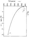
- FIG. 3 shows the dependency of the temperature coefficient of the resistance TCR on the rhodium content in the platinum alloy, the rhodium content being stated in% by weight of the platinum alloy. It is thus possible, according to FIG. 3, to precisely adjust the temperature coefficient in the range from 1600 to 3850 ppm / K for measuring resistors based on platinum alloys by varying the rhodium content of the resistance layer; only the rhodium content of the platinum alloy is varied without changing the layer thickness, so that, for example, with a constant layer thickness of 1.1 ⁇ m and a rhodium content of 0.01%, a temperature coefficient of 3850 ppm / K (point A) is achieved; If the proportion of rhodium increases to 0.04% with the same layer thickness, a temperature coefficient of 3830 ppm / K (point B) is achieved.
- a further increase in the rhodium content to 0.16% reduces the temperature coefficient to 3750 ppm / K (point C). With a further increase in the proportion of rhodium to, for example, 10%, a temperature coefficient of 1600 ppm / K (point D) can be achieved.
Abstract
Description
Die Erfindung betrifft ein Verfahren zur Herstellung eines elektrischen Meßwiderstandes mit einem vorgegebenen Temperaturkoeffizienten für ein Widerstandsthermometer, der auf einem Träger einen Platin enthaltenden Dünnfilm als Widerstandsschicht aufweist, wobei die die Widerstandsschicht tragende Oberfläche des Trägers aus elektrisch isolierendem Werkstoff besteht.The invention relates to a method for producing an electrical measuring resistor with a predetermined temperature coefficient for a resistance thermometer, which has a platinum-containing thin film on a carrier as a resistance layer, the surface of the carrier carrying the resistance layer being made of electrically insulating material.
Aus der US-PS 4,375,056 ist ein Dünnschicht-Widerstandsthermometer mit einem vorgegebenen Temperaturkoeffizienten des Widerstandes bekannt, bei dem ein dünner elektrisch leitender Metallfilm auf ein elektrisch isolierendes Substrat aufgebracht wird, wobei die Dicke des Metallfilms im Bereich von 0,05 und 0,8 µm liegt; im Bereich dieser geringen Schichtstärke ist es möglich einen geringeren Temperaturkoeffizienten zu erzielen als beim Vollmaterial. Das Verhältnis der relativen Änderung des Temperaturkoeffizienten zur relativen Änderung der Schichtstärke ist größer als 0,01. Als Dünnschichtmaterial wird vorzugsweise ein Platinfilm eingesetzt. Ein Verfahren zur Herstellung eines solchen Meßwiderstandes ist in der US-PS 4,469,717 beschrieben.US Pat. No. 4,375,056 discloses a thin-film resistance thermometer with a predetermined temperature coefficient of resistance, in which a thin electrically conductive metal film is applied to an electrically insulating substrate, the thickness of the metal film being in the range from 0.05 and 0.8 μm lies; in the area of this small layer thickness it is possible to achieve a lower temperature coefficient than with solid material. The ratio of the relative change in the temperature coefficient to the relative change in the layer thickness is greater than 0.01. A platinum film is preferably used as the thin-layer material. A method for producing such a measuring resistor is described in US Pat. No. 4,469,717.
Aus der DE-PS 25 27 739 bzw. der entsprechenden US-PS 4,050,052 ist ein Verfahren zur Herstellung eines elektrischer Meßwiderstandes für ein Widerstandsthermometer bekannt, der auf einem Träger aus keramischem Material einen durch Zerstäubung hergestellten Platin Dünnfilm in einer Dicke von 0,1 bis 10 µm trägt, der einen vorbestimmten Temperaturkoeffizienten aufweist; der mittlere thermische Ausdehnungskoeffizient des Keramiksubstrats unterscheidet sich um weniger als +/- 30 % von demjenigen des Thermometerplatins. Als Substrat wer- den Aluminiumoxid, Berylliumoxid, Thoriumoxid, Magnesiumoxid oder ein Magne- siumsilikat eingesetzt, wobei das Substrat nach einer Wärmebehandlung weniger als 20 ppm an Metallen enthält, die in mit Platin reaktionsfähiger Form vor- liegen.From DE-PS 25 27 739 and the corresponding US-PS 4,050,052 a method for producing an electrical measuring resistor for a resistance thermometer is known which on a carrier made of ceramic material a platinum thin film produced by atomization in a thickness of 0.1 to 10 µm carries, which has a predetermined temperature coefficient; the average coefficient of thermal expansion of the ceramic substrate differs from that of the thermometer board by less than +/- 30%. Aluminum oxide, beryllium oxide, thorium oxide, magnesium oxide or a magnesium silicate are used as the substrate, the substrate after heat treatment containing less than 20 ppm of metals which are in a form which is reactive with platinum.
Aus Figur 3 des Aufsatzes "Rhodium-Platinum Alloys" von A. S. Darling in der Zeitschrift Platinum Metals Review, Seite 60, Vol. 5, 1961 ist die Funktion des Temperaturkoeffizienten einer Platinlegierung in Abhängigkeit vom Rhodiumanteil dargestellt.From Figure 3 of the article "Rhodium-Platinum Alloys" by A. S. Darling in the magazine Platinum Metals Review, page 60, Vol. 5, 1961, the function of the temperature coefficient of a platinum alloy as a function of the rhodium content is shown.
Als problematisch erweist es sich nach dem Stand der Technik, eine einfache und rasche Einstellung des gewünschten elektrischen Temperaturkoeffizienten des Widerstandes je nach Anwendungsfall - beispielsweise im Bereich von 1600 bis 3860 ppm/K-vorzunehmen, da beim Aufdampfen der Widerstandsschicht aufgrund verschiedener Dampfdrücke der aufzubringenden Materialien die gewünschte Legierung nicht mit ausreichender Sicherheit einstellbar ist, bzw. bei der Kathodenzerstäubung das Targetmaterial zuvor in der gewünschten Legierung entsprechend herzustellen ist; die Einstellung eines gewünschten Temperatur-Koeffizienten des elektrischen Widerstandes über die Variation der Schichtstärke führt dagegen aufgrund der damit verbundenen Änderung des Leiterquerschnitts der Widerstandsbahn auch zu einer Änderung der Breite oder Länge der Widerstandsbahn zwecks Anpassung an den vorgegebenen Nennwiderstand des Meßwiderstandes, woraus sich eine Änderung der Struktur der Widerstandsbahn ergibt.According to the prior art, it has proven problematic to make a simple and rapid setting of the desired electrical temperature coefficient of the resistance depending on the application, for example in the range from 1600 to 3860 ppm / K, because when the resistance layer is evaporated due to different vapor pressures of the materials to be applied the desired alloy cannot be set with sufficient certainty, or in the case of cathode sputtering the target material has to be prepared beforehand in the desired alloy; The setting of a desired temperature coefficient of the electrical resistance via the variation of the layer thickness, on the other hand, leads to a change in the width or length of the resistance path due to the associated change in the conductor cross section of the resistance path for the purpose of adaptation to the predetermined nominal resistance of the measuring resistor, which results in a change in the Structure of the resistance track results.
Aufgabe der Erfindung ist es ein Verfahren anzugeben, nach dem eine Platin-Dünnfilm-Widerstandsschicht vorgegebener Schichtstärke durch Dotierung mit Fremdatomen so behandelt wird, daß ein gewünschter elektrischer Temperaturkoeffizient im Bereich von 1600 ppm/k bis 3860 ppm/k einstellbar ist.The object of the invention is to provide a method by which a platinum thin-film resistance layer of a given layer thickness is treated by doping with foreign atoms in such a way that a desired electrical temperature coefficient can be set in the range from 1600 ppm / k to 3860 ppm / k.
Die Aufgabe wird durch die kennzeichnenden Merkmale des Anspruchs 1 gelöst. Vorteilhafte Ausgestaltungen der Erfindung sind in den Unteransprüchen angegeben.The object is achieved by the characterizing features of claim 1. Advantageous embodiments of the invention are specified in the subclaims.
In einer bevorzugten Ausführungsform des Verfahrens wird als Träger Aluminiumoxid verwendet ; es ist jedoch auch möglich, einen Träger aus einem Stahl-Substrat zu verwenden, das auf der zur Aufbringung des Platin-Dünnfilms vorgesehenen Oberfläche eine elektrisch isolierende Zwischenschicht aufweist, die aus SiO₂, BaO, Al₂O₃ und einer anorganischen, Kobalt enthaltenden Farbstoffverbindung besteht, wie sie beispielsweise in der DE-PS 34 26 804 beschrieben ist. Der Platin-Dünnfilm wird mittels Elektronenstrahlverdampfung auf den Träger aufgebracht. Das im Siebdruckverfahren aufzubringende Präparat weist vorzugsweise einen Rhodiumgehalt im Bereich von 0,1 bis 12 Gew.-%, bezogen auf den Gehalt von Platin und Rhodium im Präparat, auf. Der nach dem Verfahren hergestellte Meßwiderstand weist eine Dicke im Bereich von 0,85 bis 1,3 µm auf.In a preferred embodiment of the method, aluminum oxide is used as the carrier; However, it is also possible to use a support made of a steel substrate which has an electrically insulating intermediate layer on the surface provided for the application of the platinum thin film, which consists of SiO₂, BaO, Al₂O₃ and an inorganic, cobalt-containing dye compound, such as it is described for example in DE-PS 34 26 804. The platinum thin film is applied to the carrier by means of electron beam evaporation. The preparation to be applied by the screen printing process preferably has a rhodium content in the range from 0.1 to 12% by weight, based on the content of platinum and rhodium in the preparation. The measuring resistor produced by the method has a thickness in the range from 0.85 to 1.3 µm.
Als vorteilhaft erweist es sich, daß in dem Verfahren bisher allgemein übliche Verfahrensschritte wie das Aufdampfen der Platinschicht und das Aufbringen des Präparats im Siebdruckverfahren angewendet werden und somit preiswert und exakt auszuführen sind. Ein weiterer Vorteil ist in der einfachen Variation des Temperaturkoeffizienten des elektrischen Widerstandes durch Änderung des Rhodiumanteils im Präparat zu sehen.It has proven to be advantageous that previously common process steps, such as vapor deposition of the platinum layer and the application of the preparation in the screen printing process, are used in the process and can therefore be carried out inexpensively and precisely. Another advantage can be seen in the simple variation of the temperature coefficient of the electrical resistance by changing the rhodium content in the preparation.
Im folgenden ist der Gegenstand der Erfindung anhand der Figuren 1 bis 3 näher erläutert.
- Figur 1a
- zeigt im Längsschnitt das Substrat mit der aufgebrachten Platinschicht,
- Figur 1b
- die Platinschicht gemäß Figur 1a mit der im Siebdruckverfahren aufgebrachten Präparat-Schicht,
- Figur 1c
- die mit Rhodium legierte Meßwiderstandsschicht im Längsschnitt.
Figur 2- zeigt den Meßwiderstand in einer Draufsicht nach der Strukturierung des Widerstandsmäanders.
- Figur 3
- zeigt die Abhängigkeit des Temperaturkoeffizienten vom Rhodium-Anteil in der Meßwiderstandsschicht.
- Figure 1a
- shows in longitudinal section the substrate with the applied platinum layer,
- Figure 1b
- the platinum layer according to FIG. 1a with the preparation layer applied by screen printing,
- Figure 1c
- the measurement resistance layer alloyed with rhodium in longitudinal section.
- Figure 2
- shows the measuring resistor in a plan view after the structuring of the resistance meander.
- Figure 3
- shows the dependence of the temperature coefficient on the rhodium content in the measuring resistance layer.
Gemäß Figur 1a wird auf das aus Aluminiumoxid bestehende Substrat 1 im Elektronenstrahlverfahren oder Kathodenzerstäubungsverfahren ein Platin-Dünnfilm 2 ganzflächig aufgebracht. Nach Aufbringen des Platin-Dünnfilms 2 erfolgt gemäß Figur 1b die Aufbringung eines Präparates aus einer Lösung von Platinresinat und Kunstharz in organischen Lösungsmitteln (12,5 % Pt) und aus einer Lösung von Rhodiumsulforesinat in organischen Lösungsmitteln (5 % Rh) im Siebdruckverfahren; die genannten Lösungen sind beispielsweise unter den Bezeichnungen RP 10001/145B und MR 4511-L bei der W. C. Heraeus GmbH, Hanau, erhältlich. Nach Auftragung der Siebdruck-Schicht 3 wird diese bei einer Temperatur im Bereich von 80 bis 120°C getrocknet und anschließend bei einer Temperatur im Bereich von 800 bis 950°C eingebrannt, wobei die organischen Lösungsmittel verbrennen oder verdampfen und die Resinate zersetzt werden. Der Rhodiumgehalt der Schicht 3 liegt dabei im Bereich von 0,1 % bis 12 %, bezogen auf den Gehalt von Platin und Rhodium. Nach dem Einbrennen der Schicht 3 wird das Substrat 1 zusammen mit seinen beiden Schichten 2,3 einer Wärmebehandlung unter atmosphärischen Bedingungen in einem Ofen bei einer Temperatur im Bereich von 1000 bis 1400°C solange unterzogen, bis das Rhodium in der sich bildenden Widerstandsschicht 2′ gleichmäßig verteilt ist, wobei auch zumindest ein teilweiser Austausch der Platin-Atome aus der Schicht 3 mit Platinatomen der Schicht 2 stattfindet.According to FIG. 1a, a platinum
In einem sich anschließenden Verfahrensschritt wird die Widerstandsschicht 2′ beispielsweise durch Sputterätzen in Form eines Mäanders strukturiert.In a subsequent process step, the resistance layer 2 'is structured, for example, by sputter etching in the form of a meander.
Gemäß Figur 2 befindet sich auf dem Substrat 1 die Widerstandsschicht 2′ in Mäanderform, wobei an den Enden des Widerstands-Streifens Kontaktfelder 4,5 für äußere Anschlüsse vorgesehen sind. Die Kontaktfelder 4 und 5 sind dabei nach dem gleichen Verfahren aufgebracht wie die Widerstandsschicht 2′.According to Figure 2, the resistance layer 2 'is in a meandering shape on the substrate 1,
Figur 3 zeigt die Abhängigkeit des Temperaturkoeffizienten des Widerstandes TCR vom Rhodium-Anteil in der Platinlegierung, wobei der Rhodium-Anteil in Gewichts-% der Platinlegierung angegeben ist. Es ist somit möglich, gemäß Figur 3 durch Variation des Rhodiumanteils der Widerstandsschicht den Temperaturkoeffizienten im Bereich von 1600 bis 3850 ppm/K für Meßwiderstände auf der Basis von Platinlegierungen exakt einzustellen; es wird also lediglich der Rhodiumanteil der Platinlegierung ohne Änderung der Schichtdicke variert, so daß beispielsweise bei einer konstanten Schichtdicke von 1,1 µm mit einem Rhodiumanteil von 0,01 % ein Temperaturkoeffizient von 3850 ppm/K (Punkt A) erzielt wird; steigt der Rhodiumanteil bei gleicher Schichtdicke auf 0,04 %, so wird ein Temperaturkoeffizient von 3830 ppm/K (Punkt B) erzielt. Eine weitere Erhöhung des Rhodiumgehaltes auf 0,16 % verringert den Temperaturkoeffizienten auf 3750 ppm/K (Punkt C). Bei einer weiteren Zunahme des Rhodiumanteils auf beispielsweise 10 % läßt sich ein Temperaturkoeffizient von 1600 ppm/K (Punkt D) erzielen.FIG. 3 shows the dependency of the temperature coefficient of the resistance TCR on the rhodium content in the platinum alloy, the rhodium content being stated in% by weight of the platinum alloy. It is thus possible, according to FIG. 3, to precisely adjust the temperature coefficient in the range from 1600 to 3850 ppm / K for measuring resistors based on platinum alloys by varying the rhodium content of the resistance layer; only the rhodium content of the platinum alloy is varied without changing the layer thickness, so that, for example, with a constant layer thickness of 1.1 µm and a rhodium content of 0.01%, a temperature coefficient of 3850 ppm / K (point A) is achieved; If the proportion of rhodium increases to 0.04% with the same layer thickness, a temperature coefficient of 3830 ppm / K (point B) is achieved. A further increase in the rhodium content to 0.16% reduces the temperature coefficient to 3750 ppm / K (point C). With a further increase in the proportion of rhodium to, for example, 10%, a temperature coefficient of 1600 ppm / K (point D) can be achieved.
Claims (11)
- A method for the production of an electrical measurement resistance with a given temperature coefficient for a resistance thermometer, which has on a carrier a thin film, containing platinum, as resistance layer, in which the surface of the carrier carrying the resistance layer consists of electrically insulating material, characterised in that for the formation of the resistance layer (2′) firstly a platinum thin film (2) is deposited by evaporation or is dusted onto the substrate (1), onto which thin film a layer of a preparation containing platinum resinate and rhodium sulphoresinate is applied by screen printing, having such a rhodium content that after the drying and burning in of this screen printing layer (3) and subsequent thermal treatment of the carrier, which is thus coated, at a temperature in the range of 1000 to 1400°C, the rhodium is uniformly distributed in the resistance layer and is present in a proportion in the range of 0.01 to 10% by weight.
- A method according to Claim 1, characterised in that a ceramic is used as substrate (1).
- A method according to Claim 2, characterised in that aluminium oxide, magnesium oxide, beryllium oxide or glass ceramic is used as ceramic.
- A method according to Claim 1, characterised in that as substrate (1) a metal substrate is used, which on the surface facing the platinum thin film (2) has an electrically insulating intermediate layer.
- A method according to Claim 4, characterised in that the substrate (1) consists of steel and the electrically insulating intermediate layer consists of glass ceramic with 40-65% by weight SiO₂, 25-40% by weight BaO, 5-20% by weight Al₂O₃ and of an inorganic pigment compound containing cobalt.
- A method according to Claim 5, characterised in that ferritic steel is used as steel.
- A method according to one of Claims 1 to 6, characterised in that a preparation is used, the rhodium content of which lies in the range of 0.1 to 12% by weight, in relation to the content of platinum and rhodium in the preparation.
- A method according to one of Claims 1 to 7, characterised in that the screen printing layer (3) is dried at a temperature in the range of 80 to 120°C.
- A method according to one of Claims 1 to 8, characterised in that the screen printing layer (3) is burnt in at a temperature in the range of 800 to 950°C.
- A method according to one of Claims 1 to 9, characterised in that the platinum thin film (2) is applied in a thickness of 0.8 to 1.2 µm.
- A method according to one of Claims 1 to 10, characterised in that a resistance layer (2′) with a thickness in the range of 0.85 to 1.3 µm is produced.
Applications Claiming Priority (2)
| Application Number | Priority Date | Filing Date | Title |
|---|---|---|---|
| DE4026061 | 1990-08-17 | ||
| DE4026061A DE4026061C1 (en) | 1990-08-17 | 1990-08-17 |
Publications (3)
| Publication Number | Publication Date |
|---|---|
| EP0471138A2 EP0471138A2 (en) | 1992-02-19 |
| EP0471138A3 EP0471138A3 (en) | 1992-06-17 |
| EP0471138B1 true EP0471138B1 (en) | 1994-12-14 |
Family
ID=6412421
Family Applications (1)
| Application Number | Title | Priority Date | Filing Date |
|---|---|---|---|
| EP91102300A Expired - Lifetime EP0471138B1 (en) | 1990-08-17 | 1991-02-19 | Process for producing an electrical measuring resistor |
Country Status (3)
| Country | Link |
|---|---|
| EP (1) | EP0471138B1 (en) |
| AT (1) | ATE115761T1 (en) |
| DE (2) | DE4026061C1 (en) |
Cited By (4)
| Publication number | Priority date | Publication date | Assignee | Title |
|---|---|---|---|---|
| DE19542516C1 (en) * | 1995-11-15 | 1997-04-17 | Heraeus Sensor Gmbh | Temperature sensor |
| US5831512A (en) * | 1995-10-30 | 1998-11-03 | Heraeus Sensor-Nite Gmbh | Resistance thermometer |
| US6316752B1 (en) | 1997-10-03 | 2001-11-13 | Schaffler & Co., Gesellschaft Mbh | Heating element with screen-printed Au-Pd resinate layer and Ag-Pd contact areas with solder resistant dams |
| DE102007046900B4 (en) * | 2007-09-28 | 2011-07-21 | Heraeus Sensor Technology GmbH, 63450 | High-temperature sensor and a method for its production |
Families Citing this family (10)
| Publication number | Priority date | Publication date | Assignee | Title |
|---|---|---|---|---|
| DE4300084C2 (en) * | 1993-01-06 | 1995-07-27 | Heraeus Sensor Gmbh | Resistance thermometer with a measuring resistor |
| DE4330447C2 (en) * | 1993-09-09 | 1996-09-19 | Heraeus Sensor Gmbh | Temperature sensor with a measuring resistor in a metal jacket |
| JP3175890B2 (en) * | 1993-12-27 | 2001-06-11 | 日本碍子株式会社 | Temperature sensor |
| EP0973020B1 (en) | 1998-07-16 | 2009-06-03 | EPIQ Sensor-Nite N.V. | Electrical temperature sensor with a multilayer |
| SK284764B6 (en) * | 1999-01-18 | 2005-11-03 | Slovenská Technická Univerzita, Materiálovotechnologická | Method of heat treatment and stabilizing electric resistivity of platinum wires |
| DE19945641A1 (en) * | 1999-09-23 | 2001-04-05 | Abb Research Ltd | Resistance element for an electrical network and/or an electronic component has a resistance body made of a ceramic interspersed with metal |
| CN100359305C (en) * | 2004-04-19 | 2008-01-02 | 重庆大学 | Distributing plane winding type thermal flowmeter probe |
| CN100359306C (en) * | 2004-04-19 | 2008-01-02 | 重庆大学 | Distributing thin film circuit thermal flowmeter senser |
| DE602006006671D1 (en) | 2005-06-17 | 2009-06-18 | Merz Pharma Gmbh & Co Kgaa | DEVICE AND METHOD FOR THE FERMENTATIVE MANUFACTURE OF BIOLOGICALLY ACTIVE COMPOUNDS |
| DE102007023434B4 (en) * | 2007-05-16 | 2017-07-06 | Innovative Sensor Technology Ist Ag | RTD |
Family Cites Families (7)
| Publication number | Priority date | Publication date | Assignee | Title |
|---|---|---|---|---|
| NL83232C (en) * | 1950-06-20 | |||
| DE1180215B (en) * | 1962-05-18 | 1964-10-22 | Duerrwaechter E Dr Doduco | Solution of resinates of precious metals and / or base metals in chlorinated hydrocarbons for the production of thin precious metal layers or base metal oxide layers fired onto carrier materials for electrotechnical purposes |
| DE2527739C3 (en) * | 1975-06-21 | 1978-08-31 | W.C. Heraeus Gmbh, 6450 Hanau | Process for the production of an electrical measuring resistor for a resistance thermometer |
| US4375056A (en) * | 1980-02-29 | 1983-02-22 | Leeds & Northrup Company | Thin film resistance thermometer device with a predetermined temperature coefficent of resistance and its method of manufacture |
| US4469717A (en) * | 1980-02-29 | 1984-09-04 | Leeds & Northrup Company | Thin film resistance thermometer with a predetermined temperature coefficient of resistance and its method of manufacture |
| DE3426804A1 (en) * | 1984-07-10 | 1986-01-16 | W.C. Heraeus Gmbh, 6450 Hanau | SUBSTRATE FOR PRINTED CIRCUITS |
| US4766411A (en) * | 1986-05-29 | 1988-08-23 | U.S. Philips Corporation | Use of compositionally modulated multilayer thin films as resistive material |
-
1990
- 1990-08-17 DE DE4026061A patent/DE4026061C1/de not_active Expired - Lifetime
-
1991
- 1991-02-19 AT AT91102300T patent/ATE115761T1/en not_active IP Right Cessation
- 1991-02-19 DE DE59103868T patent/DE59103868D1/en not_active Expired - Fee Related
- 1991-02-19 EP EP91102300A patent/EP0471138B1/en not_active Expired - Lifetime
Cited By (6)
| Publication number | Priority date | Publication date | Assignee | Title |
|---|---|---|---|---|
| US5831512A (en) * | 1995-10-30 | 1998-11-03 | Heraeus Sensor-Nite Gmbh | Resistance thermometer |
| DE19542516C1 (en) * | 1995-11-15 | 1997-04-17 | Heraeus Sensor Gmbh | Temperature sensor |
| US5959524A (en) * | 1995-11-15 | 1999-09-28 | Heraeus Electro-Nite International N.V. | Temperature sensor |
| US6316752B1 (en) | 1997-10-03 | 2001-11-13 | Schaffler & Co., Gesellschaft Mbh | Heating element with screen-printed Au-Pd resinate layer and Ag-Pd contact areas with solder resistant dams |
| DE102007046900B4 (en) * | 2007-09-28 | 2011-07-21 | Heraeus Sensor Technology GmbH, 63450 | High-temperature sensor and a method for its production |
| DE102007046900C5 (en) | 2007-09-28 | 2018-07-26 | Heraeus Sensor Technology Gmbh | High-temperature sensor and a method for its production |
Also Published As
| Publication number | Publication date |
|---|---|
| ATE115761T1 (en) | 1994-12-15 |
| DE59103868D1 (en) | 1995-01-26 |
| EP0471138A2 (en) | 1992-02-19 |
| DE4026061C1 (en) | 1992-02-13 |
| EP0471138A3 (en) | 1992-06-17 |
Similar Documents
| Publication | Publication Date | Title |
|---|---|---|
| EP0471138B1 (en) | Process for producing an electrical measuring resistor | |
| DE2507731C3 (en) | Measuring resistor for resistance thermometer and process for its manufacture | |
| DE2527739C3 (en) | Process for the production of an electrical measuring resistor for a resistance thermometer | |
| DE1490927C3 (en) | Process for the production of a layer resistance element using tantalum metal | |
| CH626468A5 (en) | ||
| DE4300084C2 (en) | Resistance thermometer with a measuring resistor | |
| DE102006053689A1 (en) | sensor arrangement | |
| DE2558752C3 (en) | Process for the production of a sheet resistor as a measuring resistor for resistance thermometers | |
| DE3200901A1 (en) | METHOD FOR PRODUCING A TEMPERATURE-SENSITIVE COMPONENT | |
| CH493909A (en) | Process for producing an electrical sheet resistor | |
| DE1648241C3 (en) | Maximum thermometer for surface temperatures | |
| DE1665426A1 (en) | Ohmic resistance and process for its manufacture | |
| DE2706418C3 (en) | Process for the production of a temperature measuring resistor for a resistance thermometer | |
| DE4123249C2 (en) | Method of making a variety of matched metallic thin film resistor structures | |
| DE1790082B2 (en) | METAL FILM RESISTANT ELEMENT AND METHOD OF MANUFACTURING IT | |
| DE4243410C2 (en) | Process for producing a thin film measuring resistor | |
| DE2719045B2 (en) | Sheet resistor and method of its manufacture | |
| CH511501A (en) | Thin film resistor | |
| DE1765091A1 (en) | Process for the production of a highly constant metal film resistor | |
| DE19605469A1 (en) | Adjusting resistance temp coefft of resistor | |
| AT399960B (en) | Method for producing a temperature-dependent resistor | |
| AT405688B (en) | Resistance thermometer with a measuring resistance | |
| DE2908919B1 (en) | Method for manufacturing a thin layer temperature sensor | |
| DE2605174B2 (en) | Process for the production of thin-film resistance elements | |
| DE2029266A1 (en) | Vapour plated ceramic resistances - using alloy contg aluminium and/or copper in addition to nickel and chromium |
Legal Events
| Date | Code | Title | Description |
|---|---|---|---|
| PUAI | Public reference made under article 153(3) epc to a published international application that has entered the european phase |
Free format text: ORIGINAL CODE: 0009012 |
|
| 17P | Request for examination filed |
Effective date: 19910311 |
|
| AK | Designated contracting states |
Kind code of ref document: A2 Designated state(s): AT DE FR GB IT NL SE |
|
| PUAL | Search report despatched |
Free format text: ORIGINAL CODE: 0009013 |
|
| AK | Designated contracting states |
Kind code of ref document: A3 Designated state(s): AT DE FR GB IT NL SE |
|
| 17Q | First examination report despatched |
Effective date: 19940121 |
|
| GRAA | (expected) grant |
Free format text: ORIGINAL CODE: 0009210 |
|
| AK | Designated contracting states |
Kind code of ref document: B1 Designated state(s): AT DE FR GB IT NL SE |
|
| REF | Corresponds to: |
Ref document number: 115761 Country of ref document: AT Date of ref document: 19941215 Kind code of ref document: T |
|
| REF | Corresponds to: |
Ref document number: 59103868 Country of ref document: DE Date of ref document: 19950126 |
|
| PGFP | Annual fee paid to national office [announced via postgrant information from national office to epo] |
Ref country code: AT Payment date: 19950201 Year of fee payment: 5 |
|
| PGFP | Annual fee paid to national office [announced via postgrant information from national office to epo] |
Ref country code: DE Payment date: 19950203 Year of fee payment: 5 |
|
| GBT | Gb: translation of ep patent filed (gb section 77(6)(a)/1977) |
Effective date: 19950109 |
|
| ITF | It: translation for a ep patent filed |
Owner name: SOCIETA' ITALIANA BREVETTI S.P.A. |
|
| ET | Fr: translation filed | ||
| PLBE | No opposition filed within time limit |
Free format text: ORIGINAL CODE: 0009261 |
|
| STAA | Information on the status of an ep patent application or granted ep patent |
Free format text: STATUS: NO OPPOSITION FILED WITHIN TIME LIMIT |
|
| 26N | No opposition filed | ||
| PGFP | Annual fee paid to national office [announced via postgrant information from national office to epo] |
Ref country code: FR Payment date: 19951228 Year of fee payment: 6 |
|
| PGFP | Annual fee paid to national office [announced via postgrant information from national office to epo] |
Ref country code: SE Payment date: 19960117 Year of fee payment: 6 |
|
| PGFP | Annual fee paid to national office [announced via postgrant information from national office to epo] |
Ref country code: GB Payment date: 19960208 Year of fee payment: 6 |
|
| PG25 | Lapsed in a contracting state [announced via postgrant information from national office to epo] |
Ref country code: AT Effective date: 19960219 |
|
| ITTA | It: last paid annual fee | ||
| PGFP | Annual fee paid to national office [announced via postgrant information from national office to epo] |
Ref country code: NL Payment date: 19960229 Year of fee payment: 6 |
|
| PG25 | Lapsed in a contracting state [announced via postgrant information from national office to epo] |
Ref country code: DE Effective date: 19961101 |
|
| PG25 | Lapsed in a contracting state [announced via postgrant information from national office to epo] |
Ref country code: GB Effective date: 19970219 |
|
| PG25 | Lapsed in a contracting state [announced via postgrant information from national office to epo] |
Ref country code: SE Effective date: 19970220 |
|
| PG25 | Lapsed in a contracting state [announced via postgrant information from national office to epo] |
Ref country code: NL Effective date: 19970901 |
|
| GBPC | Gb: european patent ceased through non-payment of renewal fee |
Effective date: 19970219 |
|
| PG25 | Lapsed in a contracting state [announced via postgrant information from national office to epo] |
Ref country code: FR Effective date: 19971030 |
|
| EUG | Se: european patent has lapsed |
Ref document number: 91102300.0 |
|
| NLV4 | Nl: lapsed or anulled due to non-payment of the annual fee |
Effective date: 19970901 |
|
| REG | Reference to a national code |
Ref country code: FR Ref legal event code: ST |
|
| PG25 | Lapsed in a contracting state [announced via postgrant information from national office to epo] |
Ref country code: IT Free format text: LAPSE BECAUSE OF NON-PAYMENT OF DUE FEES Effective date: 20050219 |