EP0470498A2 - Améliorations dans de relatif à des circuits intégrés - Google Patents
Améliorations dans de relatif à des circuits intégrés Download PDFInfo
- Publication number
- EP0470498A2 EP0470498A2 EP91112897A EP91112897A EP0470498A2 EP 0470498 A2 EP0470498 A2 EP 0470498A2 EP 91112897 A EP91112897 A EP 91112897A EP 91112897 A EP91112897 A EP 91112897A EP 0470498 A2 EP0470498 A2 EP 0470498A2
- Authority
- EP
- European Patent Office
- Prior art keywords
- voltage
- reference generator
- circuit
- voltage reference
- supply
- Prior art date
- Legal status (The legal status is an assumption and is not a legal conclusion. Google has not performed a legal analysis and makes no representation as to the accuracy of the status listed.)
- Withdrawn
Links
Images


Classifications
-
- G—PHYSICS
- G11—INFORMATION STORAGE
- G11C—STATIC STORES
- G11C5/00—Details of stores covered by group G11C11/00
- G11C5/14—Power supply arrangements, e.g. power down, chip selection or deselection, layout of wirings or power grids, or multiple supply levels
- G11C5/147—Voltage reference generators, voltage or current regulators; Internally lowered supply levels; Compensation for voltage drops
Definitions
- This invention relates to integrated circuits, and in particular to integrated circuit devices formed in a semiconductor substrate, for example memory devices such as dynamic random access memories.
- VLSI Dynamic Random Access Memory
- a further object is to provide a circuit which performs adequately at power up.
- the pump circuit includes:
- the pump circuit further includes:
- the integrated circuit device may include means for biasing the device substrate, said starter circuit being energized when said biasing means is active.
- an integrated circuit device includes:
- the circuitry for writing and reading information is supplied by said voltage reference generator output.
- the initialization circuit has a starter circuit connected to the input of the voltage reference generator and to an external voltage supply to initially couple the input of the reference generator to the external voltage supply and thereby start the reference generator. It also has a pump circuit. the pump circuit is connected to the input of the voltage reference generator and to the external voltage supply. It is coupled to the output of the reference generator. The pump circuit pumps a fixed charge from the external voltage supply into the voltage reference generator. Such a circuit may be incorporated into a semiconductor memory device having an on chip voltage reference generator.
- the device receives external VDD of typically 5 volts.
- On chip internal voltage regulation powers the memory arrays at 3.3 volts and the periphery circuits at 4.0 volts to reduce power consumption and channel hot carrier effects.
- the substrate is biased at -2 volts.
- the organization is bond programmable X1/X4.
- the X1 or X4 option may be selected during manufacture by putting in place a bond wire between bond pad 25 (FIG. 6) and V ss for a X1 device and omitting the bond wire for a X4 device.
- the resulting pin outs for the ten options may be seen in FIG. 2.
- the bond wire may be run between pad 25 and the V ss bus 3 of the lead frame (FIG. 3).
- the enhanced page mode is the preferred option, with a metal mask programmable option for a write per bit (data mask) operation.
- the preferred option for the refresh scheme is 4096 cycles at 64ms.
- the DRAM is bond programmable for 2048 cycle refresh.
- Option selection may be achieved in a way analogous to that employed for the X1 or X4 option selection.
- the relevant bond pad is 4, bonded to V ss for 2K refresh, otherwise the 4K refresh option is exercised.
- Test mode entry 1 is through WCBR with no address key for 16X internal parallel test with mode data compare.
- Test mode entry 2 is WCBR with over-voltage and address key only thereafter (8 volts on A11). Exit from test mode occurs from any refresh cycle (CBR or RAS only).
- Test mode entry 1 is the industry standard 16X parallel test. This test is similar to those used on the 1 MB and 4MB DRAMS, except that 16 bits are compared simultaneously instead of 8 bits. The valid address keys are A0, A1, A2, and A6.
- Test mode entry 2 contains numerous tests. There is a 32X parallel test with data compare and a 16X parallel test with data compare. Different hexadecimal addresses are keyed for the different parallel tests.
- a storage cell stress test and a VDD margin test allows connection of the external VDD to internal VARY and VPERI device supply lines through the P-channel devices.
- Other tests include a redundancy signature test, a row redundancy roll call test, a column redundancy roll call test, a row transfer test, a word-line leakage detection test, clear concurrent test modes, and a reset to normal mode.
- the DRAM also contains a test validation method that indicates if it has remained in a test mode.
- the DRAM contains redundancy features for defect elimination. It has four redundant rows per 256K memory block. All four may be used at one time. There are 3 decoders per redundant row and 11 row addresses per redundant row decoder. It uses fuses for row redundancy with, on-average, 10 fuses blown for a single repair. The row redundancy uses a two stage programmable concept to more efficiently to enable repair. There are 12 redundant columns per quadrant and four decoders per redundant column. There are 8 column addresses and 3 row addresses per decoder. The total fuse count for column repair is about, on average, 10 fuses blown for a single repair. Column redundancy also has a two-stage programmable feature to more efficiently enable repair.
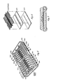
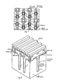
- FIG. 7 is a top view of the capacitor cell layout.
- the bit lines are poly-3 (TiSi 2 ) polyside. No bitline reference is used and the bitlines are triple twisted for noise immunity.
- the supply line voltage is about 3.3 volts.
- the word lines are segmented poly-2. They are strapped every 64 bits with metal 2.
- the memory cells are of the modified trench capacitor type and may be formed by a process such as disclosed in United States Patent 5,017,506 and European Patent Application 0410288.
- the dimensions include a 1.6um bit-line pitch by 3.0um double word line pitch, with a cell size of about 4.8uM 2 obtained through 0.6 micron technology.
- the trench opening is about 1.1 um and the trench depth is about 6.0um.
- the dielectric is of nitride/oxide, having a thickness of about 65A. Field plate isolation is utilized.
- the transistors have thin gate oxide.
- FIG. 8 is a cross-sectional view of the modified trench capacitor cell and FIG. 9 is a side view of the trench capacitor cell.
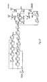
- FIG. 10 shows the overall arrangement for generating VDDREF and how it is used in the DRAM.
- the starter circuit VREFINIT(1) receives a signal RID, present during the initial power up phase of the device, to switch the external supply voltage VDD to the band gap voltage reference generator 20 to start the generator.
- the start up circuit also receives a signal BOSC from an oscillator which is activated as power up continues. This oscillator is used to drive a pump to, in turn, drive the output VDDREF even after RID has gone to the inactive state.
- the oscillator producing BOSC may conveniently be the same oscillator that is used initially to bias the device substrate. At the end of power up the signal BOSC will thus cease.
- a signal PBOSC is available to drive the main power VDDREF.
- the oscillator which forms part of the power supply charge pump may conveniently be used.
- the oscillator of the pump which supplies the substrate bias when the device is in a standby mode is employed.
- the supply used for the access circuits to the DRAM array is available and is used as an output to VDDREF for reference purposes.
- the supply fed to the bank gap generator is thus decoupled from changes in external supply VDD once the device is powered up. This contrasts with the normal arrangement of using VDD itself to supply the bandgap generator.
- Multiplier 21 supplies the various circuits as shown. During normal operations VREFINIT is inactive, however, where BOSC is the oscillator of the substrate bias booster pump, VREFINIT may be energized in its charge pumping configuration, whenever the substrate bias detector energizes the booster. Since VREFINIT operates in parallel with VDDREF, extra supply capability is available during substrate boost.
- the circuits of FIG. 10 will now be considered in more detail.
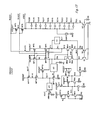
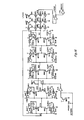
- FIG. 11 illustrates the Voltage Reference Initialization circuit VREFINIT.
- N-channel transistor MN1 is connected between Node N1 and the input signal RID.
- the gate of transistor MN1 is connected to VPERI.
- P-channel transistor MP2 is connected between external VDD and Node N1.
- the gate of P-channel transistor MP2 is connected to VDD.
- P-channel transistor MP3 is connected to between VDD and Node N1.
- the gate of P-channel transistor MP3 is connected to Node N2.
- the gates of P-channel transistors MP4 and MP5 are connected to Node N1.
- the source and drain of transistor MP4 is connected to VDD.
- One terminal of transistor MP5 is connected to VDD.
- the other terminal is connected to Node N2.
- Node N2 is connected to the gate of N-channel transistor C1.
- transistor C1 The source and drain of transistor C1 are connected to VSS.
- Node N1 is connected to the gate of N-channel low threshold voltage transistor MN6.
- Transistor MN6 is connected between Node N2 and VSS.
- Node N2 is connected to the input of inverter IV1.
- the output of the inverter IV1 is connected to Node N3.
- Inverter IV1 is biased by VDD.
- Node N3 is connected to the input of inverter IV2.
- Inverter IV2 is biased by VDD. Its output is connected to the inputs of NOR gate NR1 and NR2.
- BOSC - is connected to the input of NOR gate NR1 and is coupled to the input of NOR gate NR2 through inverter IV3.
- Inverter IV3 and NOR gates NR1 and NR2 are biased by VDD.
- the output of Nor gate NR1 is connected to Node N8.
- the output of Node NR2 is connected to N6.
- N-channel low threshold voltage transistor MN7 is connected between Node N3 and Node N9. Its gate is connected to VDD.
- Node N9 is connected to the gate of N-channel transistor MN8. It's source and drain are connected to Node N8.
- N-channel low threshold voltage transistor MN9 is connected between VDD and VDDREF. It's gate is connected to Node N9.
- N-channel low threshold voltage transistor MN10 is connected between Node N3 and Node N7. Its gate is connected to VDD.
- Node N7 is connected to the gate of N-channel transistor MN11.
- the source and drain of transistor MN11 are connected to Node N6.
- Node N7 is also connected to the gate of N-channel low threshold Voltage transistor MN12.
- Transistor MN12 is connected between VDD and VDDREF.
- the gate of N-channel transistor MNC13 is connected to VDDREF.
- the source and drain of transistor MNC13 are connected to VSSREG.
- FIG. 12 illustrates the VDD Reference circuit VDDREF.
- Signal PBOSC is coupled through inverter IV1 to Node N1.
- Node N1 is coupled through the serially connected inverter IV2, and delay stages XD1, XD2, and XD3 to an input of NAND gate ND1.
- Node N1 is directly connected to the other input of NAND gate ND1.
- Node N1 is directly connected to one input of NOR gate NR1. It is coupled through the serially connected delay stages XD4, XD5, and XD6 and inverter IV3 to the other input of NOR gate NR1.
- the output of NOR gate NR1 is coupled through inverter IV6 to one input of NAND gate ND2.
- the other input to NAND gate ND2 is the output of NAND gate ND1.
- VDDREF of the output of NAND gate ND2 is coupled through inverter IV7 to Node N16.
- Node N 16 is connected to the gates of P-channel transistor MP6 and N-channel transistor MN7.
- Transistors MP6 and MN7 are respectively connected between Node N22 and VSS.
- Low-threshold voltage N-channel transistor MN9 is connected between VDD and Node N22. Its gate is connected to VPERI.
- P-channel transistor MP10 and N-channel transistor MN11 are connected respectively between Node N22 and VSS.
- the gates of P-channel transistor NP10 and N-channel transistor MN11 are connected to the series connection between transistor MP6 and MN7.
- N-channel low threshold voltage transistor MN5 and N-channel low threshold voltage transistor Mn1 are connected respectively between VDD and BDDREF.
- the gate of transistor Mn5 is connected to VPERI.
- the gate of transistor MN1 is connected to Node N21.
- the gate of N-channel transistor MN8 is connected to the series connection of transistors MN5 and Mn1.
- the source and drain of transistor Mn8 are connected to the series connection of transistors M10 and MN11.
- Los-threshold voltage N-channel transistor MN4 is connected between VPERI and node N21.
- the gate of N-channel transistor MN3 is connected to Node N21.
- the source and drain of transistor MN3 are connected together and connected to the output of inverter IV11. Node N16 is coupled through inverter IV10 to the input of inverter IV11.
- the circuit that generates the supply to the reference voltage generator is shown in figures 11 and 12.
- the circuit in Figure 12 operates once the on-chip regulated supply has powered up and provides the isolation to the reference voltage generation from external voltage slews.
- the circuit in FIG. 11 operates only during initial power up and is turned off once the chip has reached stable operation. Since the circuit in FIG. 12 depends on the on-chip regulated supply, some initial source of power is needed for the reference voltage generator so the on-chip regulated supply can be established.
- a filtered supply is provided for the reference voltage generator that draws its power from the on-chip regulated supply, in such a way that the two will not collapse together should the on-chip regulated supply vary somewhat.
- the supply to the reference voltage generator will not vary with the external slew.
- PBOSC is a signal that comes from the oscillator used to generate the substrate bias voltage. This signal has a typical period of oscillation of approximately 1 us with approximately 505 duty cycle.
- the circuitry comprised if IV1, IV2, IV3, IV6, XD1-SD6, NR1 and ND1-ND2 is used to generate a positive pulse of approximately 12ns duration at N15 on each transition of PBOSC.
- the remainder of the circuit in FIG. 1 forms a charge pump to supply charge to the reference voltage generator and capacitor MNC13 in FIG. 11 is used to smooth the voltage ripple seen by this generator.
- capacitor MN8 charges to VPERI-Vt.
- VPERI the voltage that this capacitor can charge to
- the dependence on the external Vdd is eliminated.
- N19 and N21 are bootstrapped, thus pumping charge onto VDDREF, the supply to the reference voltage generator.
- Devices MN5 and MN9 have their drains connected to external Vdd to reduce the load on VPERI and further stabilize the on-chip regulated supply.
- BOSC - is an oscillator input that is generated only during initial power up or whenever the substrate bias voltage becomes too positive. This circuit is intended only to initialize VDDREF so that VPERI can initially be generated.
- RID is a control signal that powers up high and remains high until the internal supplies are stabilized. Once this occurs RID goes low and remains low for as long as the chip is powered up.
- NR1-NR2 are gates that allow BOSC - to charge smoothing capacitor MNC13 to Vdd during initial power up. Once RID goes low, these gates prevent BOSC_ from reactivating charging to Vdd.
- Circuitry consisting of MN1, MP2, MP3, MP4, MP5 MN6 and C1 is designed to cause N2 to power up low prior to RID being established at its initial high state.
- MN9 and MN12 are bootstrapped, each on alternate states of BOSC_, such that VDDREF is charged to Vdd during the period of time that RID is high.
- This circuit generates a reference voltage. Besides providing a stable voltage, it is designed to have immunity towards changes in temperature. A standard BANDGAP REFERENCED BIASING circuit is improved to achieve this.
- the bandgap referenced biasing circuit is comprised of transistors, MP1 through MP6, MN1 through Mn4 and Q1 through Q3. Constant current that follows along the 3 electrical path is governed by the equation;
- VREF a regulated voltage
- the parameters that generate VREF are temperature dependent parameters.
- VREF changes with temperature.
- R1 is first determined by fixing the constant current to the region of 0.5uA. Through simulation, the operation of VREF is to be 1.2V and R1 and R2 are to be 5.4 Kohms and 51.3 Kohms respectively.
- the new circuit is designed to start its voltage regulation of a Vt lower than the standard circuit.
- the gate is tied to a point of magnitude that is about one Vt potential above the drain potential.
- the device is activated into its saturation region as Vgs is activated with Vds is one Vt below Vgs.
- the device is operational at a lower voltage level.
- gate of MP1/MP2 is tied to drain of MP5
- gate of MN1/MN2 is tied to drain of MN3
- gate of MN4/MN5 tied to drain of MP4 with R4 to provide to potential drops
- gate of MP4/MP5 tied to drain of MN4 with R3 to provide the potential drops.
- the first low voltage starter drives current into R4 and then the drain of MN3 at low external voltage.
- This circuit is comprised of MP17, MP18, MP19, MP110 and MN16.
- MP17 and MP18 off current is driven into node N13 through MP19 with MN16 keeping node N117 low.
- MP110 is used to discharge capacitor MN16 when the external supply goes too low. But when the external voltage is sufficient to turn on the Bandgap Referenced Biasing transistors, Mp17 and MP18 are turn one, thus charging up M16 and turning off mP19. This allows the normal biasing mode to operate.
- the second low voltage starter sinks current from the drain of MP5.
- C1 keeps N15 low, thus turning on MP10 and MN8. This helps to switch on MP5 and MP2. By so doing, it forces current to flow in them.
- two other signals are routed for use in other circuits. They are the BIAS1 and BIAS2 signals. They are used to generate a similar current flow in other circuits through the current mirror effect.
- VMULT uses the concept of a potential divider to multiply VREF to the required voltage levels.
- a constant current source is generated at node N3 of the source coupled pair, M3 and M4.
- the gate of M3 is connected to VREF, and the gate of M4 is connected to node VREFO of a series of resistors.
- This source couple pair compares the voltage VREF and VREFO. Differential voltages cause different current flows in M3 and M4. With this current mirror, it will try to maintain the same current flowing through M3 and M4, thus maintaining the same current.
- the circuit maintains VREFO to equal to VREF.
- R2 and R3 are trimable resistors in order to achieve the required levels of 3.3V and 4V.
- Capacitor CM is to provide damping to the feedback node N1.
- the oscillator BOSC uses external voltage VDD (VEXT) as supply.
- VDD external voltage
- the oscillator provides square waveforms of 3MHz.
- the circuit is designed with seven inverters connected in feedback loop to produce a ring oscillator.
- One stage having a different transfer ratio to the oscillator can start up automatically when power is applied.
- BOSC is gated on and off by VBS_ which is controlled by VBBDET, the substrate bias voltage detector circuit. Thus, when VBB is insufficient, VBS_ will be low and BOSC will be activated. BOSC drives the booster pump VBBPB which generates the substrate bias during power up.
- An externally applied signal EXTODS can be used to disable the oscillator, and indirectly their pumps if substrate bias is to be applied externally.
- This oscillator generates a square wave signal which drives the low power or the standby VBB pump.
- a loop of five inverters is used to provide a signal of about 1 usec cycle time, 1 MHz.
- These inverters are designed with programmable sizing of the P-channel and N-channel transistors. This enables adjustment of oscillator frequency when needed, achieving the required cycle time by controlling the W/L ratio of the inverters.
- the resulting waveform has a slow rise and fall time.
- a set of 3 modified inverters is connected to the output of the loop, ie node N5. These inverters amplify the signal, increasing the rise and fall times until a square wave is generated.
- the oscillating signal can be inhibited by injecting a high level signal at probe pad EXTODS. This breaks the loop of inverters and forces node N5 to a low potential. Thus, the output LPOSC is forced low and becomes a static output.
- LPOSC There are two outputs, LPOSC and BPOSC.
- LPOSC is used for the VBB pump and PBOSC is used as booting signal for various parts of the device.
- transistors MN11 and MN16 are sized differently from the other inverters. This is to avoid the situation where the output is locked at an intermediate level at power up. this is accomplished by changing the D.C. transfer curve of one inverter in the loop of five inverters.
Applications Claiming Priority (2)
| Application Number | Priority Date | Filing Date | Title |
|---|---|---|---|
| US56052390A | 1990-07-31 | 1990-07-31 | |
| US560523 | 1990-07-31 |
Publications (2)
| Publication Number | Publication Date |
|---|---|
| EP0470498A2 true EP0470498A2 (fr) | 1992-02-12 |
| EP0470498A3 EP0470498A3 (en) | 1993-06-09 |
Family
ID=24238157
Family Applications (1)
| Application Number | Title | Priority Date | Filing Date |
|---|---|---|---|
| EP19910112897 Withdrawn EP0470498A3 (en) | 1990-07-31 | 1991-07-31 | Improvements in or relating to integrated circuits |
Country Status (1)
| Country | Link |
|---|---|
| EP (1) | EP0470498A3 (fr) |
Cited By (6)
| Publication number | Priority date | Publication date | Assignee | Title |
|---|---|---|---|---|
| EP0669619A2 (fr) * | 1994-02-25 | 1995-08-30 | Kabushiki Kaisha Toshiba | Circuit intégré à semi-conducteurs pour la génération d'une source de tension d'alimentation ayant des fluctuations de tension réduites |
| EP0676857A2 (fr) * | 1994-04-11 | 1995-10-11 | Rockwell International Corporation | Technique de génération d'une référence valable pendant les transitoirs de mise en marche du système |
| EP0676856A2 (fr) * | 1994-04-11 | 1995-10-11 | Rockwell International Corporation | Convertisseur continu-continu, efficient, bien réglé, élévateur de tension, pour circuits intégrés CMO |
| EP0676855A2 (fr) * | 1994-04-11 | 1995-10-11 | Rockwell International Corporation | Système électronique discriminateur d'alimentation et avec adaptation d'alimentation |
| EP0713220A1 (fr) * | 1994-11-15 | 1996-05-22 | STMicroelectronics Limited | Circuit de tension de référence |
| WO2005013466A1 (fr) * | 2003-07-25 | 2005-02-10 | Infineon Technologies Ag | Ensemble circuit de regulation de tension et procede permettant de faire fonctionner ledit circuit |
Citations (1)
| Publication number | Priority date | Publication date | Assignee | Title |
|---|---|---|---|---|
| EP0260474A1 (fr) * | 1986-09-18 | 1988-03-23 | International Business Machines Corporation | Systèmes adaptateurs pour source d'énergie |
-
1991
- 1991-07-31 EP EP19910112897 patent/EP0470498A3/en not_active Withdrawn
Patent Citations (1)
| Publication number | Priority date | Publication date | Assignee | Title |
|---|---|---|---|---|
| EP0260474A1 (fr) * | 1986-09-18 | 1988-03-23 | International Business Machines Corporation | Systèmes adaptateurs pour source d'énergie |
Non-Patent Citations (1)
| Title |
|---|
| IBM TECHNICAL DISCLOSURE BULLETIN. vol. 29, no. 5, October 1986, NEW YORK US pages 2167 - 2168 'POWER ON CIRCUIT.' * |
Cited By (13)
| Publication number | Priority date | Publication date | Assignee | Title |
|---|---|---|---|---|
| EP0669619A2 (fr) * | 1994-02-25 | 1995-08-30 | Kabushiki Kaisha Toshiba | Circuit intégré à semi-conducteurs pour la génération d'une source de tension d'alimentation ayant des fluctuations de tension réduites |
| EP0669619A3 (fr) * | 1994-02-25 | 1995-10-04 | Toshiba Kk | |
| US5592421A (en) * | 1994-02-25 | 1997-01-07 | Kabushiki Kaisha Toshiba | Semiconductor integrated circuit for generating an internal power source voltage with reduced potential changes |
| EP0676856A2 (fr) * | 1994-04-11 | 1995-10-11 | Rockwell International Corporation | Convertisseur continu-continu, efficient, bien réglé, élévateur de tension, pour circuits intégrés CMO |
| EP0676855A2 (fr) * | 1994-04-11 | 1995-10-11 | Rockwell International Corporation | Système électronique discriminateur d'alimentation et avec adaptation d'alimentation |
| EP0676857A3 (fr) * | 1994-04-11 | 1996-08-28 | Rockwell International Corp | Technique de génération d'une référence valable pendant les transitoirs de mise en marche du système. |
| EP0676856A3 (fr) * | 1994-04-11 | 1996-09-04 | Rockwell International Corp | Convertisseur continu-continu, efficient, bien réglé, élévateur de tension, pour circuits intégrés CMO. |
| EP0676855A3 (fr) * | 1994-04-11 | 1996-09-04 | Rockwell International Corp | Système électronique discriminateur d'alimentation et avec adaptation d'alimentation. |
| EP0676857A2 (fr) * | 1994-04-11 | 1995-10-11 | Rockwell International Corporation | Technique de génération d'une référence valable pendant les transitoirs de mise en marche du système |
| EP0713220A1 (fr) * | 1994-11-15 | 1996-05-22 | STMicroelectronics Limited | Circuit de tension de référence |
| US5831302A (en) * | 1994-11-15 | 1998-11-03 | Sgs-Thomson Microelectronics Limited | Voltage reference circuit |
| WO2005013466A1 (fr) * | 2003-07-25 | 2005-02-10 | Infineon Technologies Ag | Ensemble circuit de regulation de tension et procede permettant de faire fonctionner ledit circuit |
| US7301318B2 (en) | 2003-07-25 | 2007-11-27 | Infineon Technologies Ag | Circuit arrangement for voltage adjustment |
Also Published As
| Publication number | Publication date |
|---|---|
| EP0470498A3 (en) | 1993-06-09 |
Similar Documents
| Publication | Publication Date | Title |
|---|---|---|
| EP0469587B1 (fr) | Améliorations dans ou relatives à des circuits intégrés | |
| EP0469588B1 (fr) | Générateur d'impulsion d'initialisation lors d'une mise sous tension | |
| US6292424B1 (en) | DRAM having a power supply voltage lowering circuit | |
| US5751639A (en) | DRAM having a power supply voltage lowering circuit | |
| US5345422A (en) | Power up detection circuit | |
| US6826066B2 (en) | Semiconductor memory module | |
| US5097303A (en) | On-chip voltage regulator and semiconductor memory device using the same | |
| US5398207A (en) | MOS random access memory device with an internal voltage-down converting transistor | |
| US5208776A (en) | Pulse generation circuit | |
| JPH11288588A (ja) | 半導体回路装置 | |
| JP3583482B2 (ja) | 半導体集積回路装置 | |
| US5410510A (en) | Process of making and a DRAM standby charge pump with oscillator having fuse selectable frequencies | |
| US5309446A (en) | Test validation method for a semiconductor memory device | |
| US5410507A (en) | Special mode control method for dynamic random access memory | |
| US20100329054A1 (en) | Memory Built-In Self-Characterization | |
| JPH0676569A (ja) | ダイナミックメモリ装置 | |
| JP3636968B2 (ja) | 半導体装置及びそのテスト方法 | |
| JP3810220B2 (ja) | 内部電源供給発生器を有する集積回路半導体メモリ装置 | |
| EP0470498A2 (fr) | Améliorations dans de relatif à des circuits intégrés | |
| EP0476282A2 (fr) | Améliorations dans ou relatif à des circuits intégrés | |
| JPH0785678A (ja) | 半導体集積回路 | |
| JP3722334B2 (ja) | 半導体記憶装置 | |
| JPH0712902A (ja) | 半導体集積回路 | |
| JPH08298722A (ja) | 半導体装置および半導体装置の内部電源電位の調整方法 | |
| JPH11339470A (ja) | ダイナミック型ram |
Legal Events
| Date | Code | Title | Description |
|---|---|---|---|
| PUAI | Public reference made under article 153(3) epc to a published international application that has entered the european phase |
Free format text: ORIGINAL CODE: 0009012 |
|
| AK | Designated contracting states |
Kind code of ref document: A2 Designated state(s): DE FR GB IT NL |
|
| PUAL | Search report despatched |
Free format text: ORIGINAL CODE: 0009013 |
|
| AK | Designated contracting states |
Kind code of ref document: A3 Designated state(s): DE FR GB IT NL |
|
| STAA | Information on the status of an ep patent application or granted ep patent |
Free format text: STATUS: THE APPLICATION IS DEEMED TO BE WITHDRAWN |
|
| 18D | Application deemed to be withdrawn |
Effective date: 19931210 |