EP0469789A2 - Optischer verzweigender Wellenleiter - Google Patents
Optischer verzweigender Wellenleiter Download PDFInfo
- Publication number
- EP0469789A2 EP0469789A2 EP91306808A EP91306808A EP0469789A2 EP 0469789 A2 EP0469789 A2 EP 0469789A2 EP 91306808 A EP91306808 A EP 91306808A EP 91306808 A EP91306808 A EP 91306808A EP 0469789 A2 EP0469789 A2 EP 0469789A2
- Authority
- EP
- European Patent Office
- Prior art keywords
- waveguide
- optical
- junction
- optical branching
- waveguides
- Prior art date
- Legal status (The legal status is an assumption and is not a legal conclusion. Google has not performed a legal analysis and makes no representation as to the accuracy of the status listed.)
- Granted
Links
Images


Classifications
-
- G—PHYSICS
- G02—OPTICS
- G02B—OPTICAL ELEMENTS, SYSTEMS OR APPARATUS
- G02B6/00—Light guides; Structural details of arrangements comprising light guides and other optical elements, e.g. couplings
- G02B6/10—Light guides; Structural details of arrangements comprising light guides and other optical elements, e.g. couplings of the optical waveguide type
- G02B6/12—Light guides; Structural details of arrangements comprising light guides and other optical elements, e.g. couplings of the optical waveguide type of the integrated circuit kind
- G02B6/122—Basic optical elements, e.g. light-guiding paths
- G02B6/125—Bends, branchings or intersections
Definitions
- the present invention relates to optical branching waveguides and, in particular, to integrated Y-junction waveguides for controlling the power dividing ratio.
- Photonic integrated circuits consist of active and passive optical components fabricated on a single III-V semiconductor substrate.
- PICs photonic integrated circuits
- photonic integrated circuits simplify device packaging and testing.
- prior art Y-junction waveguides perform acceptably, due to limitations of fabrication techniques, practical Y-junction or branching waveguides deviate from their ideal designs, which in turn, has deleterious effects on optical devices connected thereto.
- the wedge tip of a Y-junction waveguide typically becomes blunt, that is truncated, when processed by wet chemical etching techniques because of undercutting.
- this truncation of the wedge tip at the Y-junction results in a substantial amount of optical back-reflection as well as radiative loss. See, for example, Sasaki et al., Electronics Letters, Vol. 17 No. 3 pp. 136-8 (1989).
- Y-junction waveguide Low back-reflection and low-loss characteristics of a Y-junction waveguide are particularly attractive for monolithically integrated active optical devices because their performance is highly dependent on the loss and reflectivity properties of the Y-junction.
- distributed feedback (DFB) and distributed bragg reflector (DBR) lasers typically require optical isolation of better than 50 dB for stable single frequency oscillation.
- optical isolation should be more than 40 dB in order to suppress ripples in the gain spectrum due to residual Fabry-Perot resonances.
- prior to the present invention there have been no Y-junction or branching waveguides designed to minimize the effect of wedge tip truncation.
- a branching junction waveguide exhibiting low radiative loss and low back-reflectivity is realized by employing between the branches of the waveguide a junction region having a gradual decrease in the effective refractive index along the direction of optical propagation.
- this approach minimizes the effect of wedge tip truncation seen for an incident optical radiation by reducing the difference in the effective refractive indices at the optical interface of the truncated wedge tip, that is, the optical region between the waveguiding region (core) and the surrounding region between the branches thereof.
- a Y-junction waveguide comprising an InGaAsP straight branch waveguide and an InGaAsP side branch waveguide intersecting at an angle ⁇ is fabricated on an InP substrate.
- a gradual decrease in the effective refractive index in the junction region between the branches is achieved by decreasing the thickness of an InGaAsP region located between the branches such as to reduce the effect of the wedge tip truncation.
- a Y-junction waveguide having the above characteristic index profile in the region between the branches is monolithically integrated with an optical amplifier.
- the low back-refectivity from the Y-junction can be used to integrate optical devices requiring high optical isolation for realizing high performance photonic integrated circuits.
- a Y-junction waveguide exhibiting low radiative loss and low back-reflectivity is realized by employing between the branches of the Y-junction a region having a gradual decrease in the effective refractive index along the direction of optical propagation.
- this approach minimizes the effect of wedge tip truncation seen by an incident optical radiation by reducing the difference in the effective refractive indices at the optical interface of the truncated wedge tip, that is between the waveguiding region (core region) and the surrounding region thereof (cladding region).
- the effective refractive index between the branches specifically varies from the core index to the cladding index.
- the low-reflectivity from the Y-junction allows active devices that require high optical isolation, such as optical amplifiers, lasers and the like, to be monolithically integrated with a monitoring detector without having the deleterious effect typically observed in the prior art.
- FIG. 1 there is shown a perspective view of an optical Y-junction waveguide 100 for dividing an optical radiation 10 incident on straight branch waveguide 20 into two branches in accordance with the principles of the invention.
- Y-junction waveguide 100 shown in FIG. 1 is meant to be for illustrative purposes only.
- Equivalent Y-junction waveguides which have the desired low-reflectivity of the present Y-junction waveguide may be realized, for example, with a plurality of either input or output branching waveguides as disclosed U.S. Patent Nos. 4,850,666 and 4,846,540, which are incorporated herein by reference.
- Similar configurations may also be realized in order to divide an incident optical radiation into more than two branches from more than one optical input waveguide. It is anticipated that while the embodiments below are directed to an asymmetric waveguide with a power dividing ratio that is polarization independent, other Y-junction waveguides may be designed, which may be either asymmetric or symmetric as well as polarization dependent.
- Y-junction waveguide 100 is fabricated on substrate 30 on which a layer 40 of optical material has been formed by deposition or regrowth techniques.
- n clad of the material surrounding the waveguiding regions (cladding region) it is necessary for the effective refractive index n clad of the material surrounding the waveguiding regions (cladding region) to be less than the effective index n core of the waveguiding regions (core region) such that the structure can guide optical radiation of the appropriate wavelength by means of total internal reflection.
- the semiconductor layers are selected from III-V semiconductor materials. Other semiconductor materials, however, may be utilized which have appropriate refractive indices. Additionally, standard fabrication techniques such as metal-organic chemical vapor deposition (MOCVD) and regrowth, wet chemical etching and photolithography are employed to fabricate Y-junction waveguide 100. These fabrication techniques are well-known to those persons of ordinary skill in the art and, thus, are not discussed in detail here.
- MOCVD metal-organic chemical vapor deposition
- regrowth wet chemical etching and photolithography
- Y-junction waveguide 100 comprises straight branch waveguide 20 and side branch waveguide 50 at an angle ⁇ with straight branch waveguide 20.
- the power splitting ratio is controlled by the angle ⁇ and the widths W1 and W2 of straight branch waveguide 20 and side branch waveguide 50, respectively, near the vicinity of Y-junction area 60.
- the width W2 is narrower than the width W1 for higher optical power propagating to straight branch waveguide 20 than side branch waveguide 50, whereas ⁇ is a few degrees because of fabrication limitations and chosen in accordance with the desired power division and bending loss considerations. It should be noted that small branching angles require long side and straight branch waveguides in order to couple individual fibers to their respective output, which can increase the total length of the Y-junction waveguide.
- both straight branch waveguide 20 and side branch waveguide 50 are single mode waveguides.
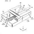
- FIG. 3 Shown in FIG. 3 is a passive Y-junction waveguide 300 in accordance with present invention integrated with an optical amplifier 310 having a gain peak wavelength near 1.55 ⁇ m.
- Optical radiation which impinges on the front facet of optical amplifier 310 is amplified by active InGaAsP layer 330 (bandgap wavelength of 1.55 ⁇ m).
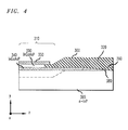
- the confined optical radiation is then coupled to adjacent InGaAsP passive straight branch waveguide 340 (bandgap wavelength of 1.3 ⁇ m), extending from the active section of the optical amplifier to the passive section of Y-junction waveguide 300, as illustrated in the cross sectional view of FIG. 4.
- Y-junction waveguide 300 comprises tapered side branch waveguide 360 at a 3.5 ° angle from straight branch waveguide 340. Additionally, both side branch waveguide 360 and straight branch waveguide 340 are passive InGaAsP waveguide mesas buried by semi-insulating InP 320.
- optical amplifier 310 With respect to optical amplifier 310, the structure is that of a semi-insulating planar buried heterostructure (SIPBH) type, with Fe doped semi-insulating InP layers 320 used for both current blocking and transverse optical confinement therein.
- Optical amplifier 310 is similar to Y-junction waveguide 300 except for active InGaAsP layer 330 and p conductivity type layers 350, which facilitates electrical contact to active region 330 of optical amplifier 310.
- Y-junction region 380 between the branches of the Y-junction has a gradual change in the effective refractive index along the Z-axis, as discussed aboveherein, to reduce the effect of the wedge tip truncation seen by an optical mode propagating therein.
- Semi-insulating InP 320 is also used as a top passive cladding waveguide region because it has a smaller absorption loss coefficient than p conductivity type layers 350.
- passive InGaAsP waveguide 340 layer and active InGaAsP layer 330 have a respective thickness of 0.35 ⁇ m and 0.9 ⁇ m.
- the widths of both the active and passive waveguides outside Y-junction region 380 are 2.5 ⁇ m.
- FIG. 5 a top plan view of Y-junction waveguide 300 is illustrated.
- the direction from straight waveguide 340 toward side waveguide 360 is taken as the Z-axis and the direction perpendicular to the plane of the drawing is taken as the Y-axis in order to define a X-Y-Z coordinate system, as shown in FIG. 5.
- the 2.5 ⁇ m width W of the straight branch waveguide 340 is tapered by a 80 ⁇ m tapering length for adiabatic mode propagation into Y-junction area 400. Power division occurs by mode conversion at the Y-junction, with the modal behavior dominated by the abrupt transition at the truncated wedge tip 410.
- the widths of the waveguides at junction tip 410 are 2.2 ⁇ m and 3.3 ⁇ m for side branch waveguide 360 and straight branch waveguide 340, respectively. Further, the width of truncated wedge tip 410 is 0.8 ⁇ m. In this exemplary structure, the widths of both waveguides are tapered back to a width W of 2.5 ⁇ m at about 100 ⁇ m outside of the Y-junction tip, as shown in FIG. 5.
- the integrated structure of the optical amplifier and Y-junction waveguide comprises three epitaxial growth steps, conventional photolithography and wet chemical etching. That is, a planar metal-organic chemical vapor deposition (MOCVD) growth for InGaAsP active layer 330 and InGaAsP passive waveguide layer (core) 340, followed by two MOCVD regrowths for InP region 320 and cap layers 350. After active layer 330 and passive waveguide layer 340 are grown on n-type InP substrate 360, 2-3 ⁇ m wide mesas are etched using a SiO2 mask in order to form active region 330, straight branch region 340 and side branch waveguide 360.
- MOCVD planar metal-organic chemical vapor deposition
- Y-junction waveguide mesas and the active waveguide mesa are etched using a SiO2 mask with the straight sections parallel to the [011] orientation.
- passive Y-junction waveguide 300 will be similar to the active section, that is optical amplifier 310, except for active layer 330 and cap layers 350.
- the total height of the active waveguide mesa is 1.5 -2 ⁇ m, and the height of the Y-junction mesa is less than 1 ⁇ m.
- a MOCVD regrowth is performed for forming semi-insulating block InP region 320.
- the active waveguide is aslo completely planarized with semi-insulating InP 320, while the passive Y-branch is covered thereby.
- the SiO2 mask is removed and cap layers 350 grown by MOCVD.
- Cap layers 350 consist of a 1.5 ⁇ m p-InP layer followed by a 0.5 ⁇ m p+ InGaAs layer.
- the processing steps are different than conventional photolithographic steps.
- the passive InGaAsP between the side branch waveguide 360 and straight branch waveguide 340 is only partially removed by a shallow etch when defining the waveguide mesas 340 and 360 as discussed above.
- a second deep etch produces the passive InGaAsP waveguide mesas.
- the thickness of the shallow etched InGaAsP layer which remains between the two branches is 0.2 ⁇ m and tapers to zero over a length of 100 ⁇ m from Y-junction tip 410.
- a reqrowth of semi-insulating InP region 320 over the InGaAsP layer buries the passive waveguides, giving the effective refractive index shown in FIGs. 6 through 10.
- the active area is covered by a third MOCVD growth of the p-InP and p InGaAs contact layers as discussed above. These layers in the passive waveguide and Y-junction areas are subsequently removed by chemical etching.
- All the etching steps above are done using standard selective etchants, such as a 2:1 mixture of HCl:H3PO4 for InP and a 3:1:1 mixture of H2 SO 4: H2O2:H2O for InGaAsP and InGaAs.
- standard selective etchants such as a 2:1 mixture of HCl:H3PO4 for InP and a 3:1:1 mixture of H2 SO 4: H2O2:H2O for InGaAsP and InGaAs.
- optical amplifier 310 is formed by depositing anti-reflective coatings on the end facets.
- optical amplifier 310 may be made into a laser either by integrating a grating in order to provide distributed feedback or by utilizing the Fabry-Perot resonances from the end facets, if made to have a sufficiently high reflectivity by subsequent coating. See, for example, K.Y Liou et al., Appl. Phys. Lett. Vol. 54 No. 2 pp. 114-6 (1989).
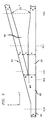
- FIG. 11 illustrates the recorded optical intensity for different planes along the waveguide in the Z-axis.
- FIG. 11 clearly shows input optical radiation being divided into two parts which evolve into two modes guided by two branching waveguides as they separate.
- the optical fields of the waveguide modes must be calculated.
- the lateral and transverse profiles of the optical fields are calculated separately by applying a separation of variables to the wave equations.
- the waveguide structure in the y-axis for straight branch waveguide 340 is a simple three layers symmetrical waveguide: a thin InGaAsP waveguide layer 340 between an InP substrate 360 and InP region 320. Accordingly, the effective refractive index may be readily obtained by solving the three-layer wave equations.
- the equivalent structure of the Y-junction waveguide can be reduced to the coupling of optical radiation from a three layer waveguide structure to an asymmetric five layer waveguide structure, as shown in FIG. 13, by using the effective refractive indices n1, n2 and n3 for the three regions of thickness d1, d2 and d3, respectively.
- the index n o is the index for InP regions 360 and 320 at the wavelength of 1.55 ⁇ m.
- the angle ⁇ can be treated by later adding a phase shift factor to the field solution of the parallel waveguide structure of FIG. 13.
- n eff ⁇ /k o
- neff ⁇ n2 case gives the higher order modes which can be neglected as will be shown later.
- E in Eq. (1) to Eq. (5) is a normalization constant given by where P is the optical power of the waveguide mode and set to 1 for simplicity in this calculation.
- straight branch waveguide 340 is a symmetrical three-layer structure, as shown in FIGS. 12 and 13.
- d2 0
- d3 0.
- Y-junction tip 410 we found that this three layer waveguide is a multimode guide.
- the mode propagating in the waveguide remains as the fundamental mode with the assumption that tapering from the input single mode guide to a multimode guide near the Y-junction area is adiabatic.
- the expressions of the magnetic field components H y (x) are the same as the expressions for E y (x) in Eq. (1) to Eq. (5) with ⁇ 1, ⁇ 3, ⁇ 0, and ⁇ 2 replaced by (- ⁇ 1/n 2 1 ), (- ⁇ 3/n 2 3 ), (- ⁇ o /n 2 0 ), and (- ⁇ 2/n 2 2 ), respectively.
- the phase factors of the types ⁇ i x and ⁇ i x in all the trigonometric, hyperbolic and exponential functions remain unchanged.
- the effective indices of the TM modes are similarly determined from the corresponding eigenvalue equation derived from the boundary conditions.
- TE polarization is conventionally defined as the electric field being parallel to the interface of the thin waveguide layer and the substrate.
- a TE mode for the three dimensional buried waveguide corresponds to TM polarization for the onedimensional waveguide structures in Figs. 12 and 13.
- the optical fields for TE modes are therefore obtained by calculating the TM fields of the lateral five-layer waveguide using TE effective indices n1, n2 and n3 of the transverse three-layer guide.
- Figs. 14, 15 and 16 show the calculated optical field amplitudes of the two lowest order modes TE00 and TE01 of the Y-branch as the two coupled waveguides separate. Only the fundamental TE00 mode is shown in the input single waveguide section. We note that TE00 mode becomes guided by straight branch waveguide 340 while the TE01 mode shifts to the side branch waveguide 360 as the separation between the two guides increases. With our waveguide structure, the higher order modes have a much smaller coupling coefficient to the input waveguide than the TE00 and TE01 modes shown in FIGs. 14 through 16. In addition, the higher order modes radiate as the two Y branches separate, where the thickness of the InGaAsP layer in the region between the two guides reduces to zero.
- Power conversion at the Y-junction can then be calculated by computing the coupling coefficients between the TE00 incident mode and the TE00 and TE01 transmitted modes.
- the coupling coefficients can be calculated by considering the Y-junction as an abrupt transition at the Y-junction tip. This is similar to the approach of the prior art for a stepped discontinuity in a single mode waveguide.
- the coupling coefficients are derived using the orthogonal relationships of the normal modes and the boundary condition in which the transverse field components are continuous at the Y-junction tip, where the single waveguide is butt coupled to the Y branches d1 and d3 with the truncation d2.
- the calculated power transmission is 0.638 for the straight branch and 0.276 for the bend branch at a 3.5° angle.
- the power splitting ratio is 2.32:1.
- the calculated power reflectivity from the Y-junction is 5.2 ⁇ 10 ⁇ 7.
- the radiation loss is 0.0863.
- the calculated power splitting ratio is 2.30:1 and the power reflectivity is 5.1 ⁇ 10 ⁇ 7.
- Equations 1 through 14 can be used for designing Y-junction waveguide with power dividing ratios other than the illustrative embodiment described hereinabove.
Applications Claiming Priority (2)
| Application Number | Priority Date | Filing Date | Title |
|---|---|---|---|
| US563162 | 1990-08-03 | ||
| US07/563,162 US5127081A (en) | 1990-08-03 | 1990-08-03 | Optical branching waveguide |
Publications (3)
| Publication Number | Publication Date |
|---|---|
| EP0469789A2 true EP0469789A2 (de) | 1992-02-05 |
| EP0469789A3 EP0469789A3 (en) | 1992-05-13 |
| EP0469789B1 EP0469789B1 (de) | 1995-10-18 |
Family
ID=24249353
Family Applications (1)
| Application Number | Title | Priority Date | Filing Date |
|---|---|---|---|
| EP91306808A Expired - Lifetime EP0469789B1 (de) | 1990-08-03 | 1991-07-25 | Optischer verzweigender Wellenleiter |
Country Status (6)
| Country | Link |
|---|---|
| US (1) | US5127081A (de) |
| EP (1) | EP0469789B1 (de) |
| JP (1) | JP3133396B2 (de) |
| CA (1) | CA2041460C (de) |
| DE (1) | DE69113909T2 (de) |
| DK (1) | DK0469789T3 (de) |
Families Citing this family (32)
| Publication number | Priority date | Publication date | Assignee | Title |
|---|---|---|---|---|
| US5265177A (en) * | 1992-05-08 | 1993-11-23 | At&T Bell Laboratories | Integrated optical package for coupling optical fibers to devices with asymmetric light beams |
| DE69228422T2 (de) * | 1992-11-24 | 1999-09-30 | Ibm | Optischer Isolator für Wellenleiter |
| DE4304993A1 (de) * | 1993-02-18 | 1994-08-25 | Sel Alcatel Ag | Verfahren zur Herstellung eines kaskadierten optischen Raumschalters und nach diesem Verfahren hergestellter kaskadierter optischer Raumschalter |
| JP3258542B2 (ja) * | 1995-07-12 | 2002-02-18 | 日本電信電話株式会社 | 分岐合流光導波路 |
| DE19605794A1 (de) * | 1996-02-16 | 1997-08-21 | Sel Alcatel Ag | Monolithisch integriertes optisches oder optoelektronisches Halbleiterbauelement und Herstellungsverfahren |
| US5770472A (en) * | 1996-09-09 | 1998-06-23 | The United States Of America As Represented By The Secretary Of The Army | Method for making monolithically integrated signal processing circuit having active and passive components |
| DE69926844T2 (de) | 1998-09-03 | 2006-06-29 | Nippon Telegraph And Telephone Corp. | Planare Lichtwellenschaltung |
| US6818559B2 (en) * | 2001-03-21 | 2004-11-16 | Intel Corporation | Method of fabrication to sharpen corners of Y-branches in integrated optical components and other micro-devices |
| US6898352B2 (en) * | 2001-05-17 | 2005-05-24 | Sioptical, Inc. | Optical waveguide circuit including passive optical waveguide device combined with active optical waveguide device, and method for making same |
| US6738546B2 (en) * | 2001-05-17 | 2004-05-18 | Sioptical, Inc. | Optical waveguide circuit including multiple passive optical waveguide devices, and method of making same |
| JP3815271B2 (ja) * | 2001-08-02 | 2006-08-30 | 日本電気株式会社 | 光結合器 |
| US20030133663A1 (en) * | 2002-01-16 | 2003-07-17 | Jds Uniphase Corporation | Integrated optical splitter |
| JP2004117706A (ja) * | 2002-09-25 | 2004-04-15 | Sumitomo Electric Ind Ltd | 光集積素子、光集積素子の製造方法、及び光源モジュール |
| US6915047B1 (en) * | 2003-03-24 | 2005-07-05 | Inplane Photonics, Inc. | Broadband, polarization independent integrated optical tap |
| US7286731B2 (en) * | 2004-04-29 | 2007-10-23 | Lucent Technologies Inc. | Monolithically integrated optical coupler with substantially no splitting loss |
| DE102005045286A1 (de) * | 2005-09-22 | 2007-04-12 | Fraunhofer-Gesellschaft zur Förderung der angewandten Forschung e.V. | Wellenleiter-integrierte Photodiode |
| KR100759805B1 (ko) * | 2005-12-07 | 2007-09-20 | 한국전자통신연구원 | 광증폭 듀플렉서 |
| JP5080227B2 (ja) * | 2007-12-13 | 2012-11-21 | 日本航空電子工業株式会社 | 光導波路素子及びその作製方法 |
| CN101883982B (zh) * | 2008-05-09 | 2013-07-03 | 松下电器产业株式会社 | 肌酸酐浓度的测定方法、测定器件及测定装置和使用这些的尿中盐分量的测定方法、测定器件及测定装置 |
| WO2011089949A1 (ja) * | 2010-01-25 | 2011-07-28 | アイアールスペック株式会社 | 化合物半導体受光素子アレイ |
| JP5145469B2 (ja) * | 2012-02-24 | 2013-02-20 | 日本航空電子工業株式会社 | 光導波路素子及びその作製方法 |
| TW201344265A (zh) * | 2012-04-27 | 2013-11-01 | Hon Hai Prec Ind Co Ltd | 脊型y分支光波導結構的製作方法 |
| TWI572917B (zh) * | 2013-02-04 | 2017-03-01 | 鴻海精密工業股份有限公司 | 極化分離器 |
| US9251819B2 (en) | 2013-11-12 | 2016-02-02 | Seagate Technology Llc | Mode converter coupling energy at a high-order transverse electric mode to a plasmonic transducer |
| US9322997B2 (en) | 2014-03-25 | 2016-04-26 | Seagate Technology Llc | Branched waveguide configuration |
| JP6047527B2 (ja) | 2014-08-14 | 2016-12-21 | 株式会社フジクラ | 基板型光導波路素子 |
| US10783917B1 (en) | 2016-11-29 | 2020-09-22 | Seagate Technology Llc | Recording head with transfer-printed laser diode unit formed of non-self-supporting layers |
| JP7047469B2 (ja) * | 2018-03-05 | 2022-04-05 | 住友大阪セメント株式会社 | 光変調器 |
| US10971179B1 (en) | 2018-04-25 | 2021-04-06 | Seagate Technology Llc | Compact mode converter having first and second straight portions for a heat-assisted magnetic recording device |
| JP7192269B2 (ja) * | 2018-06-29 | 2022-12-20 | 住友ベークライト株式会社 | 光導波路、光モジュールおよび電子機器 |
| JP7073963B2 (ja) * | 2018-07-24 | 2022-05-24 | 住友大阪セメント株式会社 | 光導波路素子 |
| US11536901B2 (en) * | 2018-08-13 | 2022-12-27 | The Regents Of The University Of Colorado, A Body Corporate | Compact and efficient integrated photonic device for coupling light on- and off-chip |
Citations (3)
| Publication number | Priority date | Publication date | Assignee | Title |
|---|---|---|---|---|
| JPS61236705A (ja) * | 1985-04-12 | 1986-10-22 | Dai Ichi Kogyo Seiyaku Co Ltd | カチオン系除草剤 |
| US4674827A (en) * | 1982-05-20 | 1987-06-23 | Masayuki Izutsu | Slab-type optical device |
| JPS62183405A (ja) * | 1986-02-08 | 1987-08-11 | Agency Of Ind Science & Technol | テ−パ付光導波回路及びその製造方法 |
Family Cites Families (3)
| Publication number | Priority date | Publication date | Assignee | Title |
|---|---|---|---|---|
| DE3687162D1 (de) * | 1985-12-10 | 1993-01-07 | Siemens Ag | Integriert-optischer multiplex-demultiplex-modul fuer die optische nachrichtenuebertragung. |
| US4846540A (en) * | 1988-01-25 | 1989-07-11 | Bell Communications Research, Inc. | Optical wavegide junction |
| US4878727A (en) * | 1988-06-30 | 1989-11-07 | Battelle Memorial Institute | Multimode channel waveguide optical coupling devices and methods |
-
1990
- 1990-08-03 US US07/563,162 patent/US5127081A/en not_active Expired - Lifetime
-
1991
- 1991-04-29 CA CA002041460A patent/CA2041460C/en not_active Expired - Lifetime
- 1991-07-25 DK DK91306808.6T patent/DK0469789T3/da active
- 1991-07-25 DE DE69113909T patent/DE69113909T2/de not_active Expired - Lifetime
- 1991-07-25 EP EP91306808A patent/EP0469789B1/de not_active Expired - Lifetime
- 1991-07-31 JP JP03190422A patent/JP3133396B2/ja not_active Expired - Lifetime
Patent Citations (3)
| Publication number | Priority date | Publication date | Assignee | Title |
|---|---|---|---|---|
| US4674827A (en) * | 1982-05-20 | 1987-06-23 | Masayuki Izutsu | Slab-type optical device |
| JPS61236705A (ja) * | 1985-04-12 | 1986-10-22 | Dai Ichi Kogyo Seiyaku Co Ltd | カチオン系除草剤 |
| JPS62183405A (ja) * | 1986-02-08 | 1987-08-11 | Agency Of Ind Science & Technol | テ−パ付光導波回路及びその製造方法 |
Non-Patent Citations (4)
| Title |
|---|
| APPLIED PHYSICS LETTERS. vol. 54, no. 2, 9 January 1989, NEW YORK US pages 114 - 116; K.-Y. LIOU ET AL.: 'Monolithic integrated InGaAsP/InP distributed feedback laser with Y-branching waveguide and a monitoring photodetector grown by metalorganic chemical vapor deposition' * |
| ELECTRONICS LETTERS. vol. 24, no. 18, 1 September 1988, ENAGE GB pages 1184 - 1185; W. Y. HUNG ET AL.: 'Novel design of wide-angle single-mode symmetric Y-junctions' * |
| PATENT ABSTRACTS OF JAPAN vol. 11, no. 93 (P-559)(2540) 24 March 1987 & JP-A-61 236 705 ( OMRON TATEISI ELECTRONICS CO. ) 4 November 1986 * |
| PATENT ABSTRACTS OF JAPAN vol. 12, no. 32 (P-661)30 January 1988 & JP-A-62 183 405 ( AGENCY OF IND. SCIENCE & TECHNOL ) 11 August 1987 * |
Also Published As
| Publication number | Publication date |
|---|---|
| EP0469789A3 (en) | 1992-05-13 |
| DK0469789T3 (da) | 1995-11-27 |
| US5127081A (en) | 1992-06-30 |
| JP3133396B2 (ja) | 2001-02-05 |
| DE69113909D1 (de) | 1995-11-23 |
| EP0469789B1 (de) | 1995-10-18 |
| DE69113909T2 (de) | 1996-04-18 |
| CA2041460A1 (en) | 1992-02-04 |
| JPH04240605A (ja) | 1992-08-27 |
| CA2041460C (en) | 1998-12-08 |
Similar Documents
| Publication | Publication Date | Title |
|---|---|---|
| EP0469789B1 (de) | Optischer verzweigender Wellenleiter | |
| US5078516A (en) | Tapered rib waveguides | |
| US5805755A (en) | Self-aligned transition from ridge to buried heterostructure waveguide, especially for multi-wavelength laser array integration | |
| US5134671A (en) | Monolithic integrated optical amplifier and photodetector | |
| Kasaya et al. | A simple laterally tapered waveguide for low-loss coupling to single-mode fibers | |
| EP1706767B1 (de) | Optische wellenkupplungsvorrichtung | |
| US7302124B2 (en) | Twin waveguide based design for photonic integrated circuits | |
| US6385376B1 (en) | Fused vertical coupler for switches, filters and other electro-optic devices | |
| US6198863B1 (en) | Optical filters | |
| US9423565B2 (en) | Coupled waveguide apparatus and structures therefor | |
| EP0725287B1 (de) | Integriertes optisches Regelelement und Verfahren zu seiner Herstellung und integriertoptisches Element und es verwendende integriertoptische Schaltkreisanordnung | |
| US6639930B2 (en) | Multi-level closed loop resonators and method for fabricating same | |
| JPH04243216A (ja) | 光導波路の製造方法ならびに光集積素子及びその製造方法 | |
| Lestra et al. | Monolithic integration of spot-size converters with 1.3-/spl mu/m lasers and 1.55-/spl mu/m polarization insensitive semiconductor optical amplifiers | |
| Bian et al. | InP-based passive ring-resonator-coupled lasers | |
| US6421492B1 (en) | Waveguide | |
| Brenner et al. | Vertically tapered InGaAsP/InP waveguides for highly efficient coupling to flat‐end single‐mode fibers | |
| Liu et al. | Fused InP-GaAs vertical coupler filters | |
| Kohtoku et al. | Control of higher order leaky modes in deep-ridge waveguides and application to low-crosstalk arrayed waveguide gratings | |
| Hayes et al. | GaAs spiral optical waveguides for delay-line applications | |
| Ishii et al. | Monolithically integrated WDM channel selectors on InP substrates | |
| Liou et al. | Y-junction power divider in InGaAsP-InP photonic integrated circuits | |
| Takeuchi et al. | Very low loss GaAs/AlGaAs miniature bending waveguide with curvature radii less than 1 mm | |
| Raburn et al. | InP-InGaAsP wafer-bonded vertically coupled X-crossing multiple channel optical add-drop multiplexer | |
| Kohtoku et al. | Spotsize converter with improved design for InP-based deep-ridge waveguide structure |
Legal Events
| Date | Code | Title | Description |
|---|---|---|---|
| PUAI | Public reference made under article 153(3) epc to a published international application that has entered the european phase |
Free format text: ORIGINAL CODE: 0009012 |
|
| AK | Designated contracting states |
Kind code of ref document: A2 Designated state(s): DE DK FR GB NL |
|
| PUAL | Search report despatched |
Free format text: ORIGINAL CODE: 0009013 |
|
| AK | Designated contracting states |
Kind code of ref document: A3 Designated state(s): DE DK FR GB NL |
|
| 17P | Request for examination filed |
Effective date: 19921023 |
|
| RAP3 | Party data changed (applicant data changed or rights of an application transferred) |
Owner name: AT&T CORP. |
|
| 17Q | First examination report despatched |
Effective date: 19940826 |
|
| GRAA | (expected) grant |
Free format text: ORIGINAL CODE: 0009210 |
|
| AK | Designated contracting states |
Kind code of ref document: B1 Designated state(s): DE DK FR GB NL |
|
| ET | Fr: translation filed | ||
| REF | Corresponds to: |
Ref document number: 69113909 Country of ref document: DE Date of ref document: 19951123 |
|
| REG | Reference to a national code |
Ref country code: DK Ref legal event code: T3 |
|
| PLBE | No opposition filed within time limit |
Free format text: ORIGINAL CODE: 0009261 |
|
| STAA | Information on the status of an ep patent application or granted ep patent |
Free format text: STATUS: NO OPPOSITION FILED WITHIN TIME LIMIT |
|
| 26N | No opposition filed | ||
| PGFP | Annual fee paid to national office [announced via postgrant information from national office to epo] |
Ref country code: DK Payment date: 20000619 Year of fee payment: 10 |
|
| PGFP | Annual fee paid to national office [announced via postgrant information from national office to epo] |
Ref country code: FR Payment date: 20010625 Year of fee payment: 11 |
|
| PGFP | Annual fee paid to national office [announced via postgrant information from national office to epo] |
Ref country code: NL Payment date: 20010717 Year of fee payment: 11 |
|
| PG25 | Lapsed in a contracting state [announced via postgrant information from national office to epo] |
Ref country code: DK Free format text: LAPSE BECAUSE OF NON-PAYMENT OF DUE FEES Effective date: 20010725 |
|
| REG | Reference to a national code |
Ref country code: GB Ref legal event code: IF02 |
|
| REG | Reference to a national code |
Ref country code: DK Ref legal event code: EBP |
|
| PG25 | Lapsed in a contracting state [announced via postgrant information from national office to epo] |
Ref country code: NL Free format text: LAPSE BECAUSE OF NON-PAYMENT OF DUE FEES Effective date: 20030201 |
|
| PG25 | Lapsed in a contracting state [announced via postgrant information from national office to epo] |
Ref country code: FR Free format text: LAPSE BECAUSE OF NON-PAYMENT OF DUE FEES Effective date: 20030331 |
|
| NLV4 | Nl: lapsed or anulled due to non-payment of the annual fee |
Effective date: 20030201 |
|
| REG | Reference to a national code |
Ref country code: FR Ref legal event code: ST |
|
| PGFP | Annual fee paid to national office [announced via postgrant information from national office to epo] |
Ref country code: DE Payment date: 20100723 Year of fee payment: 20 |
|
| PGFP | Annual fee paid to national office [announced via postgrant information from national office to epo] |
Ref country code: GB Payment date: 20100722 Year of fee payment: 20 |
|
| REG | Reference to a national code |
Ref country code: DE Ref legal event code: R071 Ref document number: 69113909 Country of ref document: DE |
|
| REG | Reference to a national code |
Ref country code: DE Ref legal event code: R071 Ref document number: 69113909 Country of ref document: DE |
|
| REG | Reference to a national code |
Ref country code: GB Ref legal event code: PE20 Expiry date: 20110724 |
|
| PG25 | Lapsed in a contracting state [announced via postgrant information from national office to epo] |
Ref country code: GB Free format text: LAPSE BECAUSE OF EXPIRATION OF PROTECTION Effective date: 20110724 |
|
| PG25 | Lapsed in a contracting state [announced via postgrant information from national office to epo] |
Ref country code: DE Free format text: LAPSE BECAUSE OF EXPIRATION OF PROTECTION Effective date: 20110726 |