EP0469638A2 - Leistungsdetektor mit einem Dünnschichtleiter - Google Patents
Leistungsdetektor mit einem Dünnschichtleiter Download PDFInfo
- Publication number
- EP0469638A2 EP0469638A2 EP91116598A EP91116598A EP0469638A2 EP 0469638 A2 EP0469638 A2 EP 0469638A2 EP 91116598 A EP91116598 A EP 91116598A EP 91116598 A EP91116598 A EP 91116598A EP 0469638 A2 EP0469638 A2 EP 0469638A2
- Authority
- EP
- European Patent Office
- Prior art keywords
- power detector
- electrode
- thermocouple
- film
- conductor
- Prior art date
- Legal status (The legal status is an assumption and is not a legal conclusion. Google has not performed a legal analysis and makes no representation as to the accuracy of the status listed.)
- Granted
Links
Images

Classifications
-
- G—PHYSICS
- G01—MEASURING; TESTING
- G01R—MEASURING ELECTRIC VARIABLES; MEASURING MAGNETIC VARIABLES
- G01R1/00—Details of instruments or arrangements of the types included in groups G01R5/00 - G01R13/00 and G01R31/00
- G01R1/20—Modifications of basic electric elements for use in electric measuring instruments; Structural combinations of such elements with such instruments
- G01R1/203—Resistors used for electric measuring, e.g. decade resistors standards, resistors for comparators, series resistors, shunts
-
- G—PHYSICS
- G01—MEASURING; TESTING
- G01R—MEASURING ELECTRIC VARIABLES; MEASURING MAGNETIC VARIABLES
- G01R19/00—Arrangements for measuring currents or voltages or for indicating presence or sign thereof
- G01R19/02—Measuring effective values, i.e. root-mean-square values
- G01R19/03—Measuring effective values, i.e. root-mean-square values using thermoconverters
-
- G—PHYSICS
- G01—MEASURING; TESTING
- G01R—MEASURING ELECTRIC VARIABLES; MEASURING MAGNETIC VARIABLES
- G01R19/00—Arrangements for measuring currents or voltages or for indicating presence or sign thereof
- G01R19/22—Arrangements for measuring currents or voltages or for indicating presence or sign thereof using conversion of AC into DC
- G01R19/225—Arrangements for measuring currents or voltages or for indicating presence or sign thereof using conversion of AC into DC by means of thermocouples or other heat sensitive elements
-
- H—ELECTRICITY
- H01—ELECTRIC ELEMENTS
- H01C—RESISTORS
- H01C1/00—Details
- H01C1/14—Terminals or tapping points specially adapted for resistors; Arrangements of terminals or tapping points on resistors
- H01C1/142—Terminals or tapping points specially adapted for resistors; Arrangements of terminals or tapping points on resistors the terminals or tapping points being coated on the resistive element
-
- H—ELECTRICITY
- H01—ELECTRIC ELEMENTS
- H01C—RESISTORS
- H01C7/00—Non-adjustable resistors formed as one or more layers or coatings; Non-adjustable resistors made from powdered conducting material or powdered semi-conducting material with or without insulating material
- H01C7/006—Thin film resistors
-
- H—ELECTRICITY
- H10—SEMICONDUCTOR DEVICES; ELECTRIC SOLID-STATE DEVICES NOT OTHERWISE PROVIDED FOR
- H10N—ELECTRIC SOLID-STATE DEVICES NOT OTHERWISE PROVIDED FOR
- H10N10/00—Thermoelectric devices comprising a junction of dissimilar materials, i.e. devices exhibiting Seebeck or Peltier effects
-
- H—ELECTRICITY
- H10—SEMICONDUCTOR DEVICES; ELECTRIC SOLID-STATE DEVICES NOT OTHERWISE PROVIDED FOR
- H10N—ELECTRIC SOLID-STATE DEVICES NOT OTHERWISE PROVIDED FOR
- H10N10/00—Thermoelectric devices comprising a junction of dissimilar materials, i.e. devices exhibiting Seebeck or Peltier effects
- H10N10/80—Constructional details
- H10N10/81—Structural details of the junction
- H10N10/817—Structural details of the junction the junction being non-separable, e.g. being cemented, sintered or soldered
Definitions
- the invention relates to a power detector comprising a thin film conductor.
- thermocouple device made by connecting a mixed crystal film of the amorphous and microcrystal phases with a metal resistance film.
- a power detector using this thermocouple device is quite capable of stable measurement during high power detection.
- this power detector comprising the thermocouple is too low in sensitivity to perform stable measurement and has poor linearity in the thermoelectromotive force of the thermocouple in detecting low power, such as 1 I.LW for example.
- thermoelectric power the Seebeck coefficient magnitude
- the invention uses an alloy thin film chiefly consisting of silicon and germanium, in which the amorphous and microcrystal phases coexist for a material constituting one of the thermocouples and utilizes the properties of the alloy thin film that the conductivity is high, the temperature coefficient of the conductivity is small, the thermoelectromotive force is large and the conductivity is substantially constant from direct current to frequencies up to 32 GHz.
- the above-mentioned alloy thin film conductor is manufactured using microelectronics processes such as the plasma CVD process and the photo assisted CVD process as indicated in U.S. Patent Application No. 068 273.
- the Si-Ge alloy thin film conductor thus produced has a crystallinity (the proportion of microcrystals to the total) of 10% to 90%.
- the microcrystals consist of silicon and germanium.
- the average grain size is about 50 to 500 ⁇ .
- the conductivity is at least 0.1 S ⁇ cm -1 .
- the ratio of conductivity change with the measuring frequency is less than 20% (less than 1 dB) from direct current to 32 GHz.
- thermocouple is made by connecting the above-mentioned alloy thin film with a conductor film.
- One or more thermocouples in combination are arranged on an insulating substrate.
- the alloy thin film in the above-mentioned thermocouple is connected with a first electrode.
- the conductor film of the thermocouple is connected with a second electrode.
- the first electrode is connected with a first beam lead electrode and the second electrode is connected with a second beam lead electrode.
- the power detector of this invention makes it possible:
- the upper limit working frequency is 18 GHz
- the detectable power range is 10 ⁇ W to 160 mW
- the detection response speed is 0.7 sec.
- the upper limit working frequency is increased to 32 GHz and the detectable power range is widened from 1 ⁇ W to 500 mW.
- the detection response speed is reduced to less than 0.06 sec.
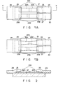
- thermocouple 24A is comprised of an Si-Ge alloy thin film conductor 22A and the metal conductor film 23A connected thereto;
- second thermocouple 24B is comprised of the Si-Ge alloy thin film conductor 22B and the metal conductor film 23B connected thereto.
- First thermocouple 24A and second thermocouple 24B are provided in parallel on insulating substrate 21 such that the Si-Ge alloy thin film of the first thermocouple and the metal film of the second thermocouple are placed facing each other, and the Si-Ge alloy thin film of the second thermocouple and the metal film of the first thermocouple are placed facing each other.
- the Si-Ge alloy thin film of the first thermocouple and the metal film of the second thermocouple are bridged by first electrode 25; the metal film of the first thermocouple is connected with second electrode 26; the Si-Ge alloy thin film of the second thermocouple is connected with third electrode 27 and thereby the outputs of the two thermocouples can be put together.
- First, second and third electrodes 25, 26 and 27 are connected tightly with beam lead electrodes 28, 29 and 30 respectively.
- the desired widths of these beam lead electrodes are wider than those of the electrodes to which the beam lead electrodes are connected and are 100 to 200 am.
- the desired thicknesses of the beam lead electrodes are 5 to 30 am, and more desirably 10 to 20 am.
- Gold or gold-plated platinum are the materials normally used for the beam lead electrodes.
- the thermal resistance between the junctions of the thermocouples is determined by the thicknesses and the widths of the insulating substrate, the Si-Ge alloy thin film conductor and the metal film.
- This thermal resistance is far greater than that of the cold junctions.
- the thermal gradient between the hot and cold junctions of the thermocouple can be increased. Therefore, by increasing the distance between the hot and cold junctions, the thermal resistance between them can be increased. As a result, the temperature difference T between them is increased.
- thermoelectromotive force V can be expressed by the thermoelectric powera a of the Si-Ge alloy thin film and the thermoelectric powera m of the metal film as follows.
- thermoelectromotive force V that is, the detection sensitivity
- T the temperature difference
- the Si-Ge alloy thin film and conductor film, constituting the thermocouples are rectangular in shape, but this invention is not limited to rectangular thermocouples.
- this invention is not limited to rectangular thermocouples.
- the number of thermocouples may be one, three or more.
- a metal was used for the conductor films in this embodiment, but other types of conducting material can be used.
- the Si-Ge alloy thin film is a p-type semiconductor, for example, the detection sensitivity can be improved by using an n-type semiconductor, which differs in pole of thermoelectric power, as a substitute for the conductor film.
- FIGs 3 and 4 show a power detection device using the power detector shown in Figure 1A.
- a transmission line is made, on dielectric substrate 31, by central conductor 32 having a specified width and outer conductors 33A and 33B disposed on both sides of the device and separated by specified distances from the central conductor 32.
- the power detector 34 has beam lead electrodes 28, 29 and 30 connected to the transmission lines, respectively, and the power being measured is suppled to the detector through the lines.
- Coupling capacitor 35 connected in series in the circuit, cuts off direct current but allows high frequency power to pass.
- Bypass capacitor 36 performs the same function as coupling capacitor 35.
- thermoelectromotive force 37 is generated as power being measured is converted into heat.
- This detection output appears as direct current at beam lead electrodes 28, 29 and 30 and is taken out by lead wires 37 and 38.
- Numeral 40 indicates a connecting part.
- the d.c. output voltage is amplified by amplifier 41 and indicated at indicator 42.
- Numeral 50 indicates the earth connection.
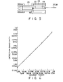
- Figure 5 is a sectional view showing the power detection device shown in Figure 3 being connected with a coaxial transmission line.
- numeral 43 indicates a hollow outer connector, into which power detection device 44 is inserted and the central conductor of coaxial transmission line 45 is connected at connecting part 46 with central conductor 33 of power detection device 44.
- Figure 6 shows the linearity of the detection sensitivity in relation to the supplied power into the power detector.
- the axis of abscissa represents the supplied power and the axis of ordinates the detection sensitivity both in logarithmic scale.
- the power detection device of this invention offers excellent linearity from low power to high power.
- One of the reasons why data with such a good linearity was obtained with high sensitivity in detecting low power is that the thermal resistance of the thermocouples was made large by using an Si-Ge alloy thin film with a thickness of about 1tim.
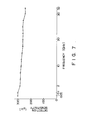
- Figure 7 shows the frequency characteristics of the detection sensitivity in the power detection device of this invention. The frequency characteristics are flat; less than 1 dB up to 32 GHz.
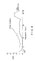
- Figure 8 shows the frequency characteristics of the VSWR (voltage standing wave ratio) in the power detector of this invention. Fine impedance matching is achieved such that the VSWR is less than 1.3 up to 32 GHz and the characteristics of the power detector of this invention are more excellent than those of the prior example indicated by the broken line in Figure 8.
Landscapes
- Engineering & Computer Science (AREA)
- Physics & Mathematics (AREA)
- General Physics & Mathematics (AREA)
- Microelectronics & Electronic Packaging (AREA)
- Power Engineering (AREA)
- Electromagnetism (AREA)
- Photometry And Measurement Of Optical Pulse Characteristics (AREA)
- Measuring Temperature Or Quantity Of Heat (AREA)
Applications Claiming Priority (3)
| Application Number | Priority Date | Filing Date | Title |
|---|---|---|---|
| JP253686/86 | 1986-10-27 | ||
| JP25368686 | 1986-10-27 | ||
| EP87906936A EP0289618B1 (de) | 1986-10-24 | 1987-10-23 | Mit einem dünnschichtleiter versehener elektrischer widerstand und kraftsensor |
Related Parent Applications (1)
| Application Number | Title | Priority Date | Filing Date |
|---|---|---|---|
| EP87906936.7 Division | 1987-10-23 |
Publications (3)
| Publication Number | Publication Date |
|---|---|
| EP0469638A2 true EP0469638A2 (de) | 1992-02-05 |
| EP0469638A3 EP0469638A3 (en) | 1992-07-08 |
| EP0469638B1 EP0469638B1 (de) | 1995-08-30 |
Family
ID=17254736
Family Applications (1)
| Application Number | Title | Priority Date | Filing Date |
|---|---|---|---|
| EP91116598A Expired - Lifetime EP0469638B1 (de) | 1986-10-27 | 1987-10-23 | Leistungsdetektor mit einem Dünnschichtleiter |
Country Status (2)
| Country | Link |
|---|---|
| EP (1) | EP0469638B1 (de) |
| DE (1) | DE3751499T2 (de) |
Cited By (1)
| Publication number | Priority date | Publication date | Assignee | Title |
|---|---|---|---|---|
| EP0935297A1 (de) * | 1998-02-06 | 1999-08-11 | Imra Europe S.A. | Thermoelektrische Peltierkühlvorrichtung |
Family Cites Families (6)
| Publication number | Priority date | Publication date | Assignee | Title |
|---|---|---|---|---|
| US3931673A (en) * | 1969-10-08 | 1976-01-13 | The United States Of America As Represented By The United States Energy Research And Development Administration | Aluminum for bonding Si-Ge alloys to graphite |
| US4442449A (en) * | 1981-03-16 | 1984-04-10 | Fairchild Camera And Instrument Corp. | Binary germanium-silicon interconnect and electrode structure for integrated circuits |
| JPS57172784A (en) * | 1981-04-17 | 1982-10-23 | Univ Kyoto | Thermoelectric conversion element |
| JPS59145582A (ja) * | 1983-02-09 | 1984-08-21 | Futaba Corp | 鉄けい化物熱電変換素子 |
| US4673957A (en) * | 1984-05-14 | 1987-06-16 | Energy Conversion Devices, Inc. | Integrated circuit compatible thin film field effect transistor and method of making same |
| JP2686928B2 (ja) * | 1985-08-26 | 1997-12-08 | アンリツ株式会社 | シリコン・ゲルマニウム混晶薄膜導電体 |
-
1987
- 1987-10-23 EP EP91116598A patent/EP0469638B1/de not_active Expired - Lifetime
- 1987-10-23 DE DE3751499T patent/DE3751499T2/de not_active Expired - Fee Related
Cited By (1)
| Publication number | Priority date | Publication date | Assignee | Title |
|---|---|---|---|---|
| EP0935297A1 (de) * | 1998-02-06 | 1999-08-11 | Imra Europe S.A. | Thermoelektrische Peltierkühlvorrichtung |
Also Published As
| Publication number | Publication date |
|---|---|
| DE3751499T2 (de) | 1996-02-22 |
| DE3751499D1 (de) | 1995-10-05 |
| EP0469638A3 (en) | 1992-07-08 |
| EP0469638B1 (de) | 1995-08-30 |
Similar Documents
| Publication | Publication Date | Title |
|---|---|---|
| US4963195A (en) | Electric resistor and a power detector both comprising a thin film conductor | |
| US3758830A (en) | Transducer formed in peripherally supported thin semiconductor web | |
| Schieferdecker et al. | Infrared thermopile sensors with high sensitivity and very low temperature coefficient | |
| USRE36615E (en) | Use of vanadium oxide in microbolometer sensors | |
| US4654622A (en) | Monolithic integrated dual mode IR/mm-wave focal plane sensor | |
| DE60117929T2 (de) | Infrarotdetektorelement und Temperaturmessgerät | |
| US6316770B1 (en) | Thermal detector with bolometric effect amplification | |
| US4782377A (en) | Semiconducting metal silicide radiation detectors and source | |
| KR100313909B1 (ko) | 적외선 센서 및 그 제조방법 | |
| US5302024A (en) | Monolithic microwave power sensor using a heat sensing diode junction | |
| Allison et al. | A bulk micromachined silicon thermopile with high sensitivity | |
| JPS60111123A (ja) | 赤外線検出器とその製造方法 | |
| US5370458A (en) | Monolithic microwave power sensor | |
| EP0645001B1 (de) | Verwendung von vanadium oxyd in mikrobolometer sensoren | |
| US6741070B2 (en) | Wide-band RF signal power detecting element and power detecting device using the same | |
| US4914042A (en) | Forming a transition metal silicide radiation detector and source | |
| EP0469638B1 (de) | Leistungsdetektor mit einem Dünnschichtleiter | |
| US4940898A (en) | Semiconducting metal silicide radiation detectors | |
| JPS5810874A (ja) | 熱電対素子 | |
| EP0099808B1 (de) | Lichtempfindliche integrierte Metalloxid-Halbleiterschaltung | |
| JPS58209174A (ja) | 熱電対素子 | |
| JP3496179B2 (ja) | 電力検出素子および電力検出装置 | |
| EP4375630A1 (de) | Pyroelektrische infrarot-detektorvorrichtung | |
| CA1326966C (en) | Semiconducting metal silicide radiation detectors | |
| Wentworth et al. | Antenna-coupled thermal detectors of mm-wave radiation |
Legal Events
| Date | Code | Title | Description |
|---|---|---|---|
| PUAI | Public reference made under article 153(3) epc to a published international application that has entered the european phase |
Free format text: ORIGINAL CODE: 0009012 |
|
| 17P | Request for examination filed |
Effective date: 19910927 |
|
| AC | Divisional application: reference to earlier application |
Ref document number: 289618 Country of ref document: EP |
|
| AK | Designated contracting states |
Kind code of ref document: A2 Designated state(s): DE FR GB IT |
|
| PUAL | Search report despatched |
Free format text: ORIGINAL CODE: 0009013 |
|
| AK | Designated contracting states |
Kind code of ref document: A3 Designated state(s): DE FR GB IT |
|
| 17Q | First examination report despatched |
Effective date: 19940725 |
|
| RBV | Designated contracting states (corrected) |
Designated state(s): DE GB |
|
| GRAA | (expected) grant |
Free format text: ORIGINAL CODE: 0009210 |
|
| AC | Divisional application: reference to earlier application |
Ref document number: 289618 Country of ref document: EP |
|
| AK | Designated contracting states |
Kind code of ref document: B1 Designated state(s): DE GB |
|
| REF | Corresponds to: |
Ref document number: 3751499 Country of ref document: DE Date of ref document: 19951005 |
|
| PLBE | No opposition filed within time limit |
Free format text: ORIGINAL CODE: 0009261 |
|
| STAA | Information on the status of an ep patent application or granted ep patent |
Free format text: STATUS: NO OPPOSITION FILED WITHIN TIME LIMIT |
|
| 26N | No opposition filed | ||
| PGFP | Annual fee paid to national office [announced via postgrant information from national office to epo] |
Ref country code: GB Payment date: 20001018 Year of fee payment: 14 |
|
| PG25 | Lapsed in a contracting state [announced via postgrant information from national office to epo] |
Ref country code: GB Free format text: LAPSE BECAUSE OF NON-PAYMENT OF DUE FEES Effective date: 20011023 |
|
| PGFP | Annual fee paid to national office [announced via postgrant information from national office to epo] |
Ref country code: DE Payment date: 20011129 Year of fee payment: 15 |
|
| REG | Reference to a national code |
Ref country code: GB Ref legal event code: IF02 |
|
| GBPC | Gb: european patent ceased through non-payment of renewal fee |
Effective date: 20011023 |
|
| PG25 | Lapsed in a contracting state [announced via postgrant information from national office to epo] |
Ref country code: DE Free format text: LAPSE BECAUSE OF NON-PAYMENT OF DUE FEES Effective date: 20030501 |