EP0465007B1 - Videosignalumschaltvorrichtung - Google Patents
Videosignalumschaltvorrichtung Download PDFInfo
- Publication number
- EP0465007B1 EP0465007B1 EP91304981A EP91304981A EP0465007B1 EP 0465007 B1 EP0465007 B1 EP 0465007B1 EP 91304981 A EP91304981 A EP 91304981A EP 91304981 A EP91304981 A EP 91304981A EP 0465007 B1 EP0465007 B1 EP 0465007B1
- Authority
- EP
- European Patent Office
- Prior art keywords
- video signal
- signal
- video
- switch
- memory
- Prior art date
- Legal status (The legal status is an assumption and is not a legal conclusion. Google has not performed a legal analysis and makes no representation as to the accuracy of the status listed.)
- Expired - Lifetime
Links
Images

Classifications
-
- H—ELECTRICITY
- H04—ELECTRIC COMMUNICATION TECHNIQUE
- H04N—PICTORIAL COMMUNICATION, e.g. TELEVISION
- H04N5/00—Details of television systems
- H04N5/76—Television signal recording
- H04N5/91—Television signal processing therefor
Definitions
- the present invention generally relates to a video signal switching apparatus and, more particularly, is directed to such an apparatus which is suitable for use in switching and displaying a plurality of video signals which are asynchronous with respect to one another.
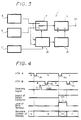
- FIG. 1 of the accompanying drawings shows an example of a prior art video signal switching apparatus.
- VTRs video tape recorders
- a home VTR for example, is not provided with a gain locking system which enables the video signal to be synchronized with an asynchronous video signal so that, as shown in Figure 2, when the video signal is simply selected, the output from the selector 10 has the discontinuity indicated in Figure 2 and the horizontal synchronizing (sync.) signal is disturbed thus resulting in disruption of the image.
- an apparatus for switching a video signal comprising:
- a video signal switching apparatus 1 to which the present invention is applied.
- video signals from a VTR-A 3 and a VTR-B 5 are input to a video memory ( a digital memory) 9 via a change-over switch (video signal switching and selecting means) 7, and an output terminal 20 and delivered to a display section (not shown) or the like.
- a change-over switch 7 is changed in position by a switching controller (switching detecting means) 13 which detects an output signal of a switching operation section 11 each time the VTR-A 3 or VTR-B 5 is selected by the switching operation section 11.
- the switching controller 13 is also supplied with output signals from the VTR-A 3 and the VTR-B 5 and supplies write (W) and read (R) timing signals through a memory controller 15 to the video memory 9 in response to the operation of the switching operation section 11 (first, second and third control means).
- the switching controller 13 is mainly formed of, for example, a microcomputer and detects vertical synchronizing signals (first and second vertical synchronizing signals, respectively) of the VTR-A 3 and the VTR-B 5 under the condition that the switching detecting signal is detected (first and second synchronizing signal detecting means).
- the VTR-A 3 outputs respective video signals a, b, c before and after two vertical synchronizing signals A 1 and A 2
- the VTR-B 5 outputs respective video signals d, e, f before and after two vertical synchronizing signals B 1 and B 2
- the switching detecting signal S occurs at the timing shown.
- the signal b will continue to be input to the video memory 9 for the time being.
- the controller 13 responds to the signal S by designating that a change-over between the signals is pending but does not immediately carry out the change-over.
- the controller 13 also monitors the signals from the VTRs for the presence of sync. pulses. Despite the occurrence of the vertical synchronizing signal B 1 of the VTR-B 5, the signal S continues to be held and the video signal b is continuously input to the video memory 9 until its vertical synchronizing signal A 2 is detected.
- the switch controller 13 operates the change-over switch 7 in accordance with the thus held signal S, thus temporarily inhibiting both the outputs from the VTR-A 3 and the VTR-B 5 being input to the video memory 9 (the level at the W terminal goes high).
- the level at the W terminal is selected to be high at least for about 10H.
- the change-over switch 7 is operated so as to input the video signal f from the VTR-B 5 to the video memory 9.
- the change-over switch 7 will not be changed in position until the input of at least the video signal b (one field time) to the video memory 9 is finished.
- the video signal f from the VTR-B 5 is input to the video memory 9 in synchronism with the vertical synchronizing signal B 2 .
- the signal written in the memory is read out therefrom on the basis of the reference clock, whereby the video signal in which neither the image signal nor the synchronizing signal are neither disturbed can be obtained at the output terminal 20.
- cut-in and cut-out may be made without changing the operation of VTR-A 3 and VTR-B 5.
- the video signal switching apparatus 1 can be utilized as a vertical blanking switch so that the video signal switching apparatus of the present invention can be applied, for example, to a camera switcher or the like.
- the timing displacement of the vertical synchronizing signals of the VTR-A 3 and VTR-B 5 is less than 10H, then the video signal f of the VTR-B 5 is not written in the memory 9 and after one field period, the next video signal g is written in the memory 9.
- one video signal of at least one field is constantly input to the video memory, while the other video signal is input to the video memory under the condition such that the input of one video signal to the video memory is completed.
- At least one field portion of a first video signal is usually inputted to the video memory, and the other video signal is inputted to the video memory once the input of the one video signal has been completed.
Landscapes
- Engineering & Computer Science (AREA)
- Multimedia (AREA)
- Signal Processing (AREA)
- Studio Circuits (AREA)
- Television Signal Processing For Recording (AREA)
- Synchronizing For Television (AREA)
Claims (5)
- Gerät zum Umschalten eines Videosignals, mit:a) einer Umschalteinrichtung (7) zum Umschalten von einem ersten Videosignal zu einem zweiten Videosignal;b) einer Speichereinrichtung (9) zum Speichern des Ausgangssignals der Umschalteinrichtung;c) einer Ermittlungseinrichtung (13) zum Speichern eines Umschaltsignals;d) einer Umschaltsteuereinrichtung (13) zum Steuern der Schalteinrichtung in Abhängigkeit vom Umschaltsignal; unde) einer Speichersteuereinrichtung (15) zum Steuern des Schreibens in die Speichereinrichtung und des Lesens aus der Speichereinrichtung in einer Weise, daß, wenn das Umschaltsignal ermittelt wird, die Speichersteuereinrichtung damit fortfährt, das erste Videosignal einzuschreiben, bis ein Sync.-Signal (Synchronisationssignal) des ersten Videosignals ermittelt wird, und nach einer vorgegebenen Periode das zweite Videosignal einschreibt, wenn ein Sync.-Signal des zweiten Videosignals ermittelt wird.
- Gerät nach Anspruch 1, wobei das Sync-Signal ein vertikales Synchronisationssignal ist.
- Gerät nach Anspruch 2, wobei die Umschaltsteuereinrichtung (13) die Umschalteinrichtung (7) so steuert, daß sie vom ersten Videosignal zum zweiten Videosignal in dem Zeitpunkt umschaltet, wenn das vertikale Synchronisationssignal des zweiten Videosignals ermittelt wird.
- Gerät nach Anspruch 1, 2 oder 3, wobei die vorgegebene Periode die Zeitdauer von 10 Horizontal-Abtastzeilenperioden ist.
- Gerät nach einem der vorhergehenden Ansprüche, wobei das erste Videosignal und das zweite Videosignal von entsprechenden Videobandrekordern reproduziert wird.
Applications Claiming Priority (2)
| Application Number | Priority Date | Filing Date | Title |
|---|---|---|---|
| JP02145875A JP3122112B2 (ja) | 1990-06-04 | 1990-06-04 | ビデオ信号切換装置 |
| JP145875/90 | 1990-06-04 |
Publications (3)
| Publication Number | Publication Date |
|---|---|
| EP0465007A2 EP0465007A2 (de) | 1992-01-08 |
| EP0465007A3 EP0465007A3 (en) | 1993-06-30 |
| EP0465007B1 true EP0465007B1 (de) | 1997-02-05 |
Family
ID=15395067
Family Applications (1)
| Application Number | Title | Priority Date | Filing Date |
|---|---|---|---|
| EP91304981A Expired - Lifetime EP0465007B1 (de) | 1990-06-04 | 1991-06-03 | Videosignalumschaltvorrichtung |
Country Status (4)
| Country | Link |
|---|---|
| US (1) | US5162903A (de) |
| EP (1) | EP0465007B1 (de) |
| JP (1) | JP3122112B2 (de) |
| DE (1) | DE69124548T2 (de) |
Families Citing this family (16)
| Publication number | Priority date | Publication date | Assignee | Title |
|---|---|---|---|---|
| JPH05336503A (ja) * | 1992-05-29 | 1993-12-17 | Sony Corp | 映像付加情報判別装置 |
| JP3392886B2 (ja) * | 1992-06-18 | 2003-03-31 | ペンタックス株式会社 | スチルビデオカメラ |
| US5619335A (en) * | 1993-09-28 | 1997-04-08 | Kabushiki Kaisha Toshiba | Digital video recording and playback system and method having multiple playback devices outputting video program data on multiple channels |
| US5798931A (en) * | 1995-06-14 | 1998-08-25 | Gilbarco Inc. | Fuel dispenser/operator intercom system |
| JPH1032810A (ja) * | 1996-07-15 | 1998-02-03 | Matsushita Electric Works Ltd | 画像処理検査装置 |
| JPH10173995A (ja) * | 1996-12-06 | 1998-06-26 | Nec Shizuoka Ltd | ビデオ信号切り替え回路 |
| US6122018A (en) * | 1997-01-17 | 2000-09-19 | Sony Corporation | Video display apparatus and method for controlling the switching of external input terminals thereof |
| US5790199A (en) * | 1997-03-06 | 1998-08-04 | International Business Machines Corporation | Method and apparatus to accommodate partial picture input to an MPEG-compliant encoder |
| US7245664B1 (en) * | 1999-05-20 | 2007-07-17 | Hitachi Kokusai Electric Inc. | Transmission control method of coded video signals and transmission system |
| EP1143715A1 (de) * | 2000-03-29 | 2001-10-10 | w + k VideoCommunication GmbH & Co. KG | Asynchrones Videoumschaltverfahren und -system |
| JP3506329B2 (ja) * | 2000-06-01 | 2004-03-15 | 松下電器産業株式会社 | 映像切替検出回路 |
| JP2004194360A (ja) * | 2004-03-22 | 2004-07-08 | Canon Inc | 撮像装置 |
| JP4164522B2 (ja) * | 2006-08-04 | 2008-10-15 | キヤノン株式会社 | 撮像装置 |
| JP6687361B2 (ja) * | 2015-10-28 | 2020-04-22 | ラピスセミコンダクタ株式会社 | 半導体装置、映像表示システムおよび映像信号の出力方法 |
| JP6788996B2 (ja) * | 2016-04-27 | 2020-11-25 | ラピスセミコンダクタ株式会社 | 半導体装置、映像表示システムおよび映像信号出力方法 |
| CN113840046B (zh) * | 2020-06-08 | 2022-11-04 | 杭州海康威视数字技术股份有限公司 | 视频轮询组轮询方法及装置 |
Family Cites Families (7)
| Publication number | Priority date | Publication date | Assignee | Title |
|---|---|---|---|---|
| GB806636A (en) * | 1955-04-12 | 1958-12-31 | Soc Nouvelle Outil Rbv Radio | Improvements to switching units in telecommunications |
| JPS6053940B2 (ja) * | 1978-05-19 | 1985-11-28 | 株式会社東京放送 | フレ−ムシンクロナイザにおける書き込み禁止制御回路 |
| JPS58213580A (ja) * | 1982-06-04 | 1983-12-12 | Nec Corp | 静止画像伝送装置 |
| GB2152321B (en) * | 1983-11-14 | 1988-01-13 | Transimage International Limit | Improvements in or relating to selection of video sources |
| US4743958A (en) * | 1986-10-06 | 1988-05-10 | The Grass Valley Group, Inc. | Multiple television standards input selector and convertor |
| US4994916A (en) * | 1988-08-25 | 1991-02-19 | Yacov Pshtissky | Apparatus and method for encoding identification information for multiple asynchronous video signal sources |
| US4890162A (en) * | 1989-01-26 | 1989-12-26 | Rca Licensing Corporation | Adjustable antialias filters |
-
1990
- 1990-06-04 JP JP02145875A patent/JP3122112B2/ja not_active Expired - Lifetime
-
1991
- 1991-05-31 US US07/708,293 patent/US5162903A/en not_active Expired - Lifetime
- 1991-06-03 EP EP91304981A patent/EP0465007B1/de not_active Expired - Lifetime
- 1991-06-03 DE DE69124548T patent/DE69124548T2/de not_active Expired - Fee Related
Also Published As
| Publication number | Publication date |
|---|---|
| DE69124548D1 (de) | 1997-03-20 |
| EP0465007A2 (de) | 1992-01-08 |
| JP3122112B2 (ja) | 2001-01-09 |
| JPH0438081A (ja) | 1992-02-07 |
| DE69124548T2 (de) | 1997-05-28 |
| EP0465007A3 (en) | 1993-06-30 |
| US5162903A (en) | 1992-11-10 |
Similar Documents
| Publication | Publication Date | Title |
|---|---|---|
| EP0465007B1 (de) | Videosignalumschaltvorrichtung | |
| EP0502673A2 (de) | Videosignalumschaltgerät | |
| US4178613A (en) | Television picture special effects system using digital memory techniques | |
| US5177618A (en) | Dual deck vcr and duplicating circuit therefor | |
| EP0279549A2 (de) | Verfahren und Gerät für digitale Videosignalverarbeitung | |
| US4764812A (en) | Selection of video sources | |
| GB2037530A (en) | Processing reproduced pal colour television signals | |
| US4698698A (en) | Digital television signal processing apparatus | |
| JP2760809B2 (ja) | テレビジョン受信機 | |
| US5617147A (en) | Transmission system for an aspect-area-ratio position ID signal | |
| CA1324659C (en) | Electronic editing apparatus | |
| US4376291A (en) | Method of compensating time faults in a digital color television signal | |
| US5305106A (en) | Image signal reproducing apparatus having a synchronizing signal generator | |
| US3878557A (en) | Color framing videotape recording apparatus and method | |
| GB2255220A (en) | Automatic index scan apparatus and method | |
| EP0227030B1 (de) | Standbildaufzeichnungsvorrichtung mit minimalisiertem Zufallsrausch | |
| US5257104A (en) | Video signal processing apparatus | |
| US4905099A (en) | Intermediate picture field storage system for variable speed magnetic tape video data read-out | |
| US5887114A (en) | Video memory device for processing a digital video signal comprising a separation means which separates a horizontal synchronizing signal from a digital video signal | |
| US5862294A (en) | Video signal reproducing apparatus in image fast locking system | |
| US5239421A (en) | Video signal processing method and apparatus with timebase disturbance correction and dropout compensation | |
| US5045944A (en) | Video signal generating circuit for use in video tape recorder and television receiver | |
| KR100405585B1 (ko) | 비디오 신호 처리 장치 | |
| JPS62169590A (ja) | 磁気記録再生装置 | |
| JP3248352B2 (ja) | 画像監視記録再生装置 |
Legal Events
| Date | Code | Title | Description |
|---|---|---|---|
| PUAI | Public reference made under article 153(3) epc to a published international application that has entered the european phase |
Free format text: ORIGINAL CODE: 0009012 |
|
| AK | Designated contracting states |
Kind code of ref document: A2 Designated state(s): DE FR GB |
|
| PUAL | Search report despatched |
Free format text: ORIGINAL CODE: 0009013 |
|
| AK | Designated contracting states |
Kind code of ref document: A3 Designated state(s): DE FR GB |
|
| 17P | Request for examination filed |
Effective date: 19931206 |
|
| 17Q | First examination report despatched |
Effective date: 19951020 |
|
| GRAG | Despatch of communication of intention to grant |
Free format text: ORIGINAL CODE: EPIDOS AGRA |
|
| GRAH | Despatch of communication of intention to grant a patent |
Free format text: ORIGINAL CODE: EPIDOS IGRA |
|
| GRAH | Despatch of communication of intention to grant a patent |
Free format text: ORIGINAL CODE: EPIDOS IGRA |
|
| GRAA | (expected) grant |
Free format text: ORIGINAL CODE: 0009210 |
|
| AK | Designated contracting states |
Kind code of ref document: B1 Designated state(s): DE FR GB |
|
| REF | Corresponds to: |
Ref document number: 69124548 Country of ref document: DE Date of ref document: 19970320 |
|
| ET | Fr: translation filed | ||
| PLBE | No opposition filed within time limit |
Free format text: ORIGINAL CODE: 0009261 |
|
| STAA | Information on the status of an ep patent application or granted ep patent |
Free format text: STATUS: NO OPPOSITION FILED WITHIN TIME LIMIT |
|
| 26N | No opposition filed | ||
| PGFP | Annual fee paid to national office [announced via postgrant information from national office to epo] |
Ref country code: DE Payment date: 20010528 Year of fee payment: 11 |
|
| PGFP | Annual fee paid to national office [announced via postgrant information from national office to epo] |
Ref country code: GB Payment date: 20010530 Year of fee payment: 11 |
|
| PGFP | Annual fee paid to national office [announced via postgrant information from national office to epo] |
Ref country code: FR Payment date: 20010611 Year of fee payment: 11 |
|
| REG | Reference to a national code |
Ref country code: GB Ref legal event code: IF02 |
|
| PG25 | Lapsed in a contracting state [announced via postgrant information from national office to epo] |
Ref country code: GB Free format text: LAPSE BECAUSE OF NON-PAYMENT OF DUE FEES Effective date: 20020603 |
|
| PG25 | Lapsed in a contracting state [announced via postgrant information from national office to epo] |
Ref country code: DE Free format text: LAPSE BECAUSE OF NON-PAYMENT OF DUE FEES Effective date: 20030101 |
|
| GBPC | Gb: european patent ceased through non-payment of renewal fee |
Effective date: 20020603 |
|
| PG25 | Lapsed in a contracting state [announced via postgrant information from national office to epo] |
Ref country code: FR Free format text: LAPSE BECAUSE OF NON-PAYMENT OF DUE FEES Effective date: 20030228 |
|
| REG | Reference to a national code |
Ref country code: FR Ref legal event code: ST |