EP0460758A2 - Logisches Gatter mit begrenzten Interferenztransienten auf den Versorgungsleitungen - Google Patents
Logisches Gatter mit begrenzten Interferenztransienten auf den Versorgungsleitungen Download PDFInfo
- Publication number
- EP0460758A2 EP0460758A2 EP91201366A EP91201366A EP0460758A2 EP 0460758 A2 EP0460758 A2 EP 0460758A2 EP 91201366 A EP91201366 A EP 91201366A EP 91201366 A EP91201366 A EP 91201366A EP 0460758 A2 EP0460758 A2 EP 0460758A2
- Authority
- EP
- European Patent Office
- Prior art keywords
- transistor
- output
- emitter
- base
- current
- Prior art date
- Legal status (The legal status is an assumption and is not a legal conclusion. Google has not performed a legal analysis and makes no representation as to the accuracy of the status listed.)
- Withdrawn
Links
Images

Classifications
-
- H—ELECTRICITY
- H03—ELECTRONIC CIRCUITRY
- H03K—PULSE TECHNIQUE
- H03K19/00—Logic circuits, i.e. having at least two inputs acting on one output; Inverting circuits
- H03K19/003—Modifications for increasing the reliability for protection
- H03K19/00346—Modifications for eliminating interference or parasitic voltages or currents
- H03K19/00353—Modifications for eliminating interference or parasitic voltages or currents in bipolar transistor circuits
-
- H—ELECTRICITY
- H03—ELECTRONIC CIRCUITRY
- H03K—PULSE TECHNIQUE
- H03K19/00—Logic circuits, i.e. having at least two inputs acting on one output; Inverting circuits
- H03K19/003—Modifications for increasing the reliability for protection
- H03K19/00307—Modifications for increasing the reliability for protection in bipolar transistor circuits
Definitions
- the present invention relates to digital logic gate circuits which employ transistors as the active switching elements, and wherein a change of logic state may cause transient variations of the potential of the internal voltage supply lines of the circuit relative to the external voltage supply to which the circuit is connected. Such variations are most troublesome in the low potential or ground line, being generally referred to as ground "bounce".
- TTL logic A problem with TTL logic is that the pull-down transistor may be driven into saturation during turn-on, which limits its turn-off speed due to storage of minority carriers in the base zone.
- a Schottky barrier diode is connected between the base and collector of the transistor and serves to clamp the base current as saturation is approached.
- Selection of the logic state in the output stage is effected by a control transistor coupled to such stage and which renders it either more conductive or less conductive depending on the logic value of the input control signal.
- the input control signal may be produced by an input circuit configured to provide a given logic function; e.g., AND, OR, NAND, etc., among a number of inputs thereto.
- the input circuit may comprise several transistors which receive respective logic signals at their bases and which have their emitters connected in common to a constant current source which also supplies current to the emitter of the control transistor of the gate circuit.
- the problem of transient ground bounce during high speed transitions between logic states of a TTL logic gate circuit may occur because the transistors in the pull-up and pull-down stages may both be conductive for a brief interval during a transition, and also because of transient currents produced in such stages due to the capacitance of the load driven by the logic gate.
- the resistance and inductance of the lines by which the gate circuit is connected to the external voltage supply and to the load are also contributing factors.
- TTL logic gate which includes clamping diodes to keep the pull-down transistor out of saturation
- U.S. Patent No. 4,501,976, issued February 26, 1985 substantially as shown in Fig. 1 herein.
- All transistors and diodes therein except pull-up transistor Q2 are of the Schottky clamped type. For purposes of illustration all transistors are shown as NPN type bipolar.
- the pull-up transistor Q2 and pull-down transistor Q1 are connected in series between internal voltage supply line 1 and internal ground line 2.
- Supply line 1 is coupled to high external voltage supply V cc , which has inherent resistance R v and inductance L v .
- the low or ground terminal of the external voltage supply V cc is coupled to the internal ground line 2, via inherent resistance R g and inductance L g .
- the collector of transistor Q2 is coupled by a resistor 4 to supply line 1.
- the logic output signal is produced at the junction 5 which provides external load 7 with output voltage V OUT .
- the latter coupling also has inherent resistance R o and inductance L o .
- the input logic control signal V IN is received from an input circuit not shown at the base of a control transistor Q3.
- the emitter of transistor Q3 is connected to the base of pull-down transistor Q1.
- the collector of transistor Q3 is connected to supply line 1 by a resistor 9, and is further connected to the base of a transistor Q4 the emitter of which is connected to the base of pull-up transistor Q2.
- the collector of transistor Q4 is connected to the collector of transistor Q2, and the emitter of transistor Q4 is connected to internal ground line 3 by a resistor 11.
- Transistors Q2 and Q4 thereby form a Darlington pair, which provides a high current gain between the base of the first Darlington transistor Q4 and the emitter of the second Darlington transistor Q2.
- a diode 13 is connected between the base of transistor Q2 and the collector of transistor Q3, and speeds turn-off of the Darlington pair when the input logic control signal V IN at the base of transistor Q3 switches from a "0" to a "1".
- the emitter of transistor Q3 is returned to internal ground line 2 by a resistor 14 in series with a diode 15 which speeds turn-off of transistor Q1 when the input logic signal V IN changes from a "1" to a "0".
- Fig. 2 is a circuit diagram of a typical ECL gate. It includes an output transistor Q5 which has its emitter connected by a resistor 29 to an internal V EE line 2 which is at a negative potential relative to the internal V cc line. The emitter of transistor Q5 drives a load 7 across which the output signal V OUT of the gate circuit is produced.
- the input logic control signal V IN is applied to the base of an input transistor Q7 the emitter of which is connected in common with the emitter of a control transistor Q9 to a constant current source 25.
- a current source may be a resistor of suitable resistance.
- the collector of transistor Q7 is returned to the internal V cc line 1, and the collector of control transistor Q9 is connected to line 1 by a resistor 30.
- transistor Q9 The base of transistor Q9 is connected to a source of a constant reference voltage V R between the V cc and V EE levels.
- Transistors Q7 and Q9 thereby form a differential amplifier for the input logic control signal V IN , producing an output at the collector of control transistor Q9 which is coupled to the base of output transistor Q5.
- the invention provides a transistor gate circuit in which transient changes in potential of the internal voltage supply lines relative to the external voltage supply to which they are coupled are limited by limiting the maximum current through the output stage of the gate. In the case of an output stage employing a bipolar transistor, this is achieved by making use of the fact that the internal base-emitter resistance causes the base-emitter voltage to increase with increasing collector-emitter current.
- Such a gate circuit includes an internal voltage supply line coupled to an external voltage supply, and at least one output stage which produces a logic output signal across a load connected thereto.
- the output stage may be a composite equivalent transistor formed by a Darlington-connected pair of transistors, the base of such output transistor being coupled to the output of a control transistor which switches the output transistor to a high or a low conductive state depending on the logic value of an input logic control signal supplied to the base of the control transistor.
- a current bypass transistor is connected with its collector-emitter path in shunt with the base-emitter path of the output transistor, the base of the bypass transistor being coupled to the base of the output transistor.
- the bypass transistor thereby diverts an increasing proportion of the base current supplied by the control transistor to the output transistor as the collector-emitter current of the output transistor increases, thereby limiting the maximum value of such current and consequently limiting the current in the path from the external voltage supply through the output transistor.
- another current bypass transistor may be provided with its collector-emitter path in shunt with the base-emitter path of the pull-down transistor so that the maximum collector-emitter current of the pull-down transistor is also limited.
- the current bypass transistor can itself be a composite equivalent transistor formed by a Darlington-connected pair of transistors.
- the invention is especially useful in bipolar saturating logic, such as, but not limited to TTL.
- bipolar saturating logic such as, but not limited to TTL.
- non-saturating logic such as ECL
- the invention is advantageous, but to a somewhat lesser degree.
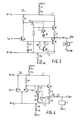
- Fig. 3 is a circuit diagram of a TTL logic circuit in accordance with the invention to provide current limitation in both output stages thereof. Corresponding elements in Figs. 1 and 3 are similarly identified.
- the current limiting arrangement for the pull-down stage comprising transistor Q1 includes a current bypass transistor Q5, the emitter of which is connected to the emitter of transistor Q1 and the collector of which is connected via resistor 17 to the base of transistor Q1.
- the base of transistor Q5 is connected by a resistor 19 to the base of transistor Q1.
- the emitter-collector path of transistor Q5 shunts the emitter-base of transistor Q1. If the collector-emitter current of transistor Q1 increases, its base voltage will rise due to the internal base-emitter resistance of transistor Q1. Consequently, the base voltage of transistor Q5 will increase, increasing its collector-emitter current.
- the circuit in Fig. 3 also includes a current limiting bypass arrangement for the pull-up output stage comprising the Darlington-connected pair of transistors Q2 and Q4.
- the emitter of transistor Q2 is connected by a resistor 21 to junction point 5, to which the collector of transistor Q1 is also connected.
- a current bypass transistor Q6 has its collector connected to the base of transistor Q4 and its emitter connected by a diode 23 to junction point 5.
- the collector-emitter path of transistor Q6 shunts the base-to-emitter path of the composite Darlington transistor formed by transistors Q2 and Q4.
- the emitter current of transistor Q2 establishes a voltage drop in resistor 21 which serves as a control voltage for transistor Q6, such voltage being proportional to such current.
- the diode 23 provides a substantially constant bias voltage for the emitter of transistor Q6 relative to junction point 5 and speeds turn-off of transistor Q6 when transistor Q4 turns off. That will occur when the input logic control signal V IN changes to a "1".
- the collector resistor 4 in Fig. 1 is not required in Fig. 3 because of the limitation on the collector current of transistor Q2.
- resistor 21 and diode 23 are needed to assure that sufficient current will be derived through bypass transistor Q6.
- Resistor 21 establishes a substantial base-emitter voltage for transistor Q2, and so also for transistor Q6.
- the forward voltage drop across diode 23 offsets to some degree the voltage across resistor 21.
- the base-emitter paths of the transistors in the pull-up and pull-down output stages are each shunted by a current bypass transistor which diverts an increasing proportion of the base drive current for such stages as the current conducted thereby increases, thereby setting a maximum limit on such current and so also limiting the potential difference or "ground bounce" between the internal ground line of the gate circuit and the terminal of the external power supply to which such line is connected.
- Such current limitation similarly limits the potential bounce between the internal supply line 1 and the external voltage supply.
- Fig. 4 is a circuit diagram of an ECL gate as in Fig. 2 modified so as to incorporate a current limiting arrangement in accordance with the invention. Corresponding elements in Figs. 2 and 4 have the same identifying numerals.
- a Darlington-connected pair of transistors Q11 and Q12 constitute a composite current bypass transistor which shunts the base-emitter path of output transistor Q5 of the gate circuit.
- the base of the first Darlington transistor Q11 is connected to the base of output transistor Q5 and the emitter of the second Darlington transistor Q12 is connected to junction point 5 to which the emitter of transistor Q5 is also connected by a resistor 31.
- the emitter of transistor Q11 is connected to the base of transistor Q12 by a resistor 32, and the collectors thereof are connected in common by a resistor 33 to the base of transistor Q5.
- the base of transistor Q12 is connected to its emitter by a resistor 34.
- transistor Q5 As the collector-emitter current of transistor Q5 increases its base-emitter voltage will increase and the voltage across resistor 31 will also increase, thereby rendering the Darlington pair Q11 and Q12 increasingly conductive and so diverting an increasing proportion of the base current supplied to transistor Q5 from the collector of transistor Q9.
- a maximum limit is thereby established for the collector-emitter current of transistor Q5, and so the magnitude of the transient voltage which can be produced due to the resistance and inductance of the couplings to the external V cc supply and the external ground is also limited.
- the resistor 31 connected between the emitter of output transistor Q5 and junction point 5 serves to establish sufficient base-emitter voltage to allow the Darlington pair Q11 and Q12 to turn on, thereby limiting the base current supplied to transistor Q5.
Landscapes
- Physics & Mathematics (AREA)
- Engineering & Computer Science (AREA)
- Computer Hardware Design (AREA)
- Computing Systems (AREA)
- General Engineering & Computer Science (AREA)
- Mathematical Physics (AREA)
- Logic Circuits (AREA)
- Electronic Switches (AREA)
Applications Claiming Priority (2)
| Application Number | Priority Date | Filing Date | Title |
|---|---|---|---|
| US534773 | 1990-06-07 | ||
| US07/534,773 US5159213A (en) | 1990-06-07 | 1990-06-07 | Logic gate circuit with limited transient bounce in potential of the internal voltage supply lines |
Publications (2)
| Publication Number | Publication Date |
|---|---|
| EP0460758A2 true EP0460758A2 (de) | 1991-12-11 |
| EP0460758A3 EP0460758A3 (en) | 1992-01-22 |
Family
ID=24131477
Family Applications (1)
| Application Number | Title | Priority Date | Filing Date |
|---|---|---|---|
| EP19910201366 Withdrawn EP0460758A3 (en) | 1990-06-07 | 1991-06-04 | Logic gate circuit with limited transient bounce in potential of the internal voltage supply lines |
Country Status (3)
| Country | Link |
|---|---|
| US (1) | US5159213A (de) |
| EP (1) | EP0460758A3 (de) |
| JP (1) | JPH04233324A (de) |
Families Citing this family (5)
| Publication number | Priority date | Publication date | Assignee | Title |
|---|---|---|---|---|
| DE4031350A1 (de) * | 1990-10-04 | 1992-04-09 | Bosch Gmbh Robert | Spannungsbegrenzung fuer eine transistorschaltung |
| JP2928651B2 (ja) * | 1991-03-19 | 1999-08-03 | 株式会社日立製作所 | 通信機能を備えた制御装置 |
| DE4222170C1 (de) * | 1992-07-06 | 1993-09-23 | Siemens Ag, 80333 Muenchen, De | |
| US6157205A (en) * | 1998-11-23 | 2000-12-05 | Cirrus Logic, Inc. | Grounding scheme for a high-speed data channel |
| US6695845B2 (en) * | 2000-10-16 | 2004-02-24 | Robert A Dixon | Method and apparatus utilizing interference fit screw shanks for nonmetallic spinal stabilization |
Family Cites Families (17)
| Publication number | Priority date | Publication date | Assignee | Title |
|---|---|---|---|---|
| JPS50109656A (de) * | 1974-02-01 | 1975-08-28 | ||
| FR2494936A1 (fr) * | 1980-11-21 | 1982-05-28 | Thomson Csf | Commutateur a commande par impulsions en ouverture et en fermeture et son integration |
| US4424455A (en) * | 1982-04-22 | 1984-01-03 | Motorola, Inc. | Glitch eliminating data selector |
| US4504928A (en) * | 1982-08-30 | 1985-03-12 | Motorola, Inc. | Current ramp generator |
| US4521699A (en) * | 1982-09-10 | 1985-06-04 | Advanced Micro Devices, Inc. | High-speed schottky TTL gate apparatus |
| US4616144A (en) * | 1983-01-12 | 1986-10-07 | Kabushiki Kaisha Toshiba | High withstand voltage Darlington transistor circuit |
| JPS60254823A (ja) * | 1984-05-30 | 1985-12-16 | Mitsubishi Electric Corp | 半導体集積回路装置 |
| IT1221009B (it) * | 1984-12-28 | 1990-06-21 | Sgs Ates Componenti Elettonici | Circuito di comando ad alto rendimento,integrato monoliticamente,per la commutazione di transistori |
| US4704548A (en) * | 1985-01-31 | 1987-11-03 | Texas Instruments Incorporated | High to low transition speed up circuit for TTL-type gates |
| DE3621396A1 (de) * | 1986-06-26 | 1988-01-14 | Bosch Gmbh Robert | Transistoranordnung mit einem endstufentransistor |
| JPS6378617A (ja) * | 1986-09-22 | 1988-04-08 | Mitsubishi Electric Corp | バイポ−ラ論理回路 |
| JPS63115420A (ja) * | 1986-10-31 | 1988-05-20 | Mitsubishi Electric Corp | バイポ−ラ論理回路 |
| JPS63265461A (ja) * | 1986-12-15 | 1988-11-01 | Fuji Electric Co Ltd | 半導体装置 |
| US4746817A (en) * | 1987-03-16 | 1988-05-24 | International Business Machines Corporation | BIFET logic circuit |
| US4893032A (en) * | 1987-03-23 | 1990-01-09 | International Business Machines Corp. | Non-saturating temperature independent voltage output driver with adjustable down level |
| US4896058A (en) * | 1988-04-26 | 1990-01-23 | North American Philips Corp. | TTL circuit having ramped current output |
| US4970620A (en) * | 1989-08-23 | 1990-11-13 | General Motors Corporation | FET bridge protection circuit |
-
1990
- 1990-06-07 US US07/534,773 patent/US5159213A/en not_active Expired - Fee Related
-
1991
- 1991-06-04 JP JP3132985A patent/JPH04233324A/ja active Pending
- 1991-06-04 EP EP19910201366 patent/EP0460758A3/en not_active Withdrawn
Also Published As
| Publication number | Publication date |
|---|---|
| JPH04233324A (ja) | 1992-08-21 |
| EP0460758A3 (en) | 1992-01-22 |
| US5159213A (en) | 1992-10-27 |
Similar Documents
| Publication | Publication Date | Title |
|---|---|---|
| US4845386A (en) | Bi-MOS logic circuit having a totem pole type output buffer section | |
| US4698525A (en) | Buffered Miller current compensating circuit | |
| US4376900A (en) | High speed, non-saturating, bipolar transistor logic circuit | |
| JPH04233325A (ja) | 高速ttlバッファ回路及びラインドライバ | |
| US5159213A (en) | Logic gate circuit with limited transient bounce in potential of the internal voltage supply lines | |
| US4037115A (en) | Bipolar switching transistor using a Schottky diode clamp | |
| JPH0629824A (ja) | 論理信号切り換え回路 | |
| US4931673A (en) | ECL-to-TTL translator circuit with ground bounce protection | |
| US4883975A (en) | Schmitt trigger circuit | |
| US5059827A (en) | ECL circuit with low voltage/fast pull-down | |
| EP0098155B1 (de) | Schmitt-Trigger-Schaltung | |
| US4165494A (en) | Bi-state linear amplifier | |
| US4501976A (en) | Transistor-transistor logic circuit with hysteresis | |
| US4593210A (en) | Switching circuit with active pull-off | |
| US5066871A (en) | Maximum swing cascode circuit for a bipolar charge pump | |
| US4584490A (en) | Input circuit for providing discharge path to enhance operation of switching transistor circuits | |
| EP0285157A2 (de) | Tri-state-Ausgangsschaltung | |
| US5066876A (en) | Circuit for converting ecl level signals to mos level signals | |
| US3828202A (en) | Logic circuit using a current switch to compensate for signal deterioration | |
| EP0076099B1 (de) | TTL-Schaltung | |
| US4631422A (en) | TTL circuit with a clamping transistor for speedy turn-off of output transistor | |
| EP0427084B1 (de) | Cascodeschaltkreis mit maximalem Hub für eine bipolare Ladungspumpe | |
| USRE27804E (en) | Transistor-transistor logic circuits having improved voltage transfer characteristics | |
| US4777391A (en) | Bipolar multiplexer having a select buffer circuit with a charging and discharging circuit | |
| US4259599A (en) | Complementary transistor switching circuit |
Legal Events
| Date | Code | Title | Description |
|---|---|---|---|
| PUAI | Public reference made under article 153(3) epc to a published international application that has entered the european phase |
Free format text: ORIGINAL CODE: 0009012 |
|
| PUAL | Search report despatched |
Free format text: ORIGINAL CODE: 0009013 |
|
| AK | Designated contracting states |
Kind code of ref document: A2 Designated state(s): DE FR GB |
|
| AK | Designated contracting states |
Kind code of ref document: A3 Designated state(s): DE FR GB |
|
| 17P | Request for examination filed |
Effective date: 19920722 |
|
| 17Q | First examination report despatched |
Effective date: 19950707 |
|
| STAA | Information on the status of an ep patent application or granted ep patent |
Free format text: STATUS: THE APPLICATION IS DEEMED TO BE WITHDRAWN |
|
| 18D | Application deemed to be withdrawn |
Effective date: 19960619 |