EP0285157A2 - Tri-state-Ausgangsschaltung - Google Patents
Tri-state-Ausgangsschaltung Download PDFInfo
- Publication number
- EP0285157A2 EP0285157A2 EP88105267A EP88105267A EP0285157A2 EP 0285157 A2 EP0285157 A2 EP 0285157A2 EP 88105267 A EP88105267 A EP 88105267A EP 88105267 A EP88105267 A EP 88105267A EP 0285157 A2 EP0285157 A2 EP 0285157A2
- Authority
- EP
- European Patent Office
- Prior art keywords
- tri
- field effect
- output
- transistors
- type
- Prior art date
- Legal status (The legal status is an assumption and is not a legal conclusion. Google has not performed a legal analysis and makes no representation as to the accuracy of the status listed.)
- Granted
Links
Images
Classifications
-
- H—ELECTRICITY
- H03—ELECTRONIC CIRCUITRY
- H03K—PULSE TECHNIQUE
- H03K19/00—Logic circuits, i.e. having at least two inputs acting on one output; Inverting circuits
- H03K19/20—Logic circuits, i.e. having at least two inputs acting on one output; Inverting circuits characterised by logic function, e.g. AND, OR, NOR, NOT circuits
-
- H—ELECTRICITY
- H03—ELECTRONIC CIRCUITRY
- H03K—PULSE TECHNIQUE
- H03K19/00—Logic circuits, i.e. having at least two inputs acting on one output; Inverting circuits
- H03K19/02—Logic circuits, i.e. having at least two inputs acting on one output; Inverting circuits using specified components
- H03K19/08—Logic circuits, i.e. having at least two inputs acting on one output; Inverting circuits using specified components using semiconductor devices
- H03K19/094—Logic circuits, i.e. having at least two inputs acting on one output; Inverting circuits using specified components using semiconductor devices using field-effect transistors
- H03K19/09425—Multistate logic
- H03K19/09429—Multistate logic one of the states being the high impedance or floating state
-
- H—ELECTRICITY
- H03—ELECTRONIC CIRCUITRY
- H03K—PULSE TECHNIQUE
- H03K19/00—Logic circuits, i.e. having at least two inputs acting on one output; Inverting circuits
- H03K19/02—Logic circuits, i.e. having at least two inputs acting on one output; Inverting circuits using specified components
- H03K19/08—Logic circuits, i.e. having at least two inputs acting on one output; Inverting circuits using specified components using semiconductor devices
- H03K19/094—Logic circuits, i.e. having at least two inputs acting on one output; Inverting circuits using specified components using semiconductor devices using field-effect transistors
- H03K19/0944—Logic circuits, i.e. having at least two inputs acting on one output; Inverting circuits using specified components using semiconductor devices using field-effect transistors using MOSFET or insulated gate field-effect transistors, i.e. IGFET
- H03K19/09448—Logic circuits, i.e. having at least two inputs acting on one output; Inverting circuits using specified components using semiconductor devices using field-effect transistors using MOSFET or insulated gate field-effect transistors, i.e. IGFET in combination with bipolar transistors [BIMOS]
Definitions
- the present invention relates to a tri-state output circuit using bipolar transistors and complementary field effect transistors, and operable with low power consumption, high load driving capability and at high speed.
- tri-state output circuits which can take three output conditions, i.e., high and low level conditions and a high impedance condition at the output terminal of the circuit.
- These tri-state output circuits include a TTL circuit construction using bipolar transistors and a CMOS circuit construction using CMOS transistors, which are one kind of complementary FET (field effect transistor).
- the tri-state output circuit When the tri-state output circuit is constructed with a TTL circuit construction, a circuit having a high load driving capability and operable at high speed can be realized due to its large transfer conductance, which is one feature of bipolar transistors.
- the tri-state output circuit is constructed with a CMOS circuit construction
- the power consumption can be reduced, to be sure.
- the transfer conductance of MOS transistors is small, compared with that of bipolar transistors, the load driving capability is decreased, which in turn results in a detrimental effect in the high speed operation of the circuit.
- the ON-time resistance of the transistors is decreased.
- the ON-time resistance of the transistors can no longer absorb the overshoot or the undershoot of the output signal in a resonance circuit, which contains an inductance component of the wiring leads connected to the output terminal and a capacitance component of a load, thereby producing the "ringing". This will bring about, in the worst case, a malfunction.
- One feature of the tri-state output circuit resides in the provisions of an input section having a NOR gate circuit receptive of an input signal and a tri-state signal for taking a NOR logical sum, and an invertor circuit receptive of the tri-state signal for producing an inverted signal thereof, each of the circuits consisting of a plurality of complementary field effect transistors; a control section having a first type first field effect transistor and a second type second field effect transistor, each of gate terminals thereof being commonly connected to the output terminal of the invertor circuit, each of the source terminals thereof being connected to either a power supply or to the ground potential respectively, a second type third field effect transistor having its gate terminal being connected to an output terminal of the NOR gate circuit and its source being connected to the ground potential, a first electric current control circuit having a plurality of second type field effect transistors coupled to the first, second and third field effect transistors as well as the input and tri-state terminals, and a second electric current control circuit having a plurality of second
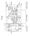
- a single figure indicates one embodiment of the tri-state output circuit according to the present invention.
- the tri-state output circuit consists of an input section I for receiving an input signal and a tri-state signal, the input section I being consisted of a plurality of complementary types of P-channel and N-channel field effect transistors (FETs), a control section II for receiving an output signal from the input section I, which is also consisted of the P-channel and N-channel FETs, and an output section III for producing an inverted output of the input signal and a high impedance output condition, which is consisted of NPN transistors and which is controlled by the control section II.
- FETs P-channel and N-channel field effect transistors
- the input section I more specifically comprises a NOR gate 1 for taking a NOR logical sum of the input signal and tri-state signal, and an invertor 2 for producing an inverted output of the tri-state signal.
- the NOR gate 1 comprises the P-channel FET P1 and the N-channel FET N1, with each of the gate terminals commonly connected to the input terminal IN to which the input signal is applied and P2 and N2, with each of the gate terminals applied by the tri-state signal.
- the P1 and P2 are connected in parallel between the power supply V CC and the output terminal 3 of the NOR gate 1, while N1 and N2 are connected in series between the output terminal 3 and the ground (potential).
- the invertor 2 comprises P3 and N3, with each of the gate terminals commonly connected to the tri-state terminal T to which the tri-state signal is applied.
- P3 is connected between the power supply V CC and the output terminal 4 of the invertor while N3 is connected between the output terminal 4 and the ground.
- the control section II comprises P4, N4, N5, a first current control circuit 5 and a second current control circuit 6.
- P4 and N4 have each gate terminal commonly connected to the output terminal 4 of the invertor 2 and each source terminal connected to either the V CC or the ground, respectively.
- N5 has its gate terminal connected to the output terminal 3 of the NOR gate 1 and its source terminal connected to the ground.
- the first current control circuit 5 comprises N6 and N7, with each gate terminal connected to the input terminal IN, and N8 and N9 with each gate terminal connected to the tri-state terminal T.
- N6 and N9, and N8 and N7 are connected in series respectively, while N6 and N7 and N8 and N9 each are connected in parallel.
- the second current control circuit 6 likewise comprises N10, N11, N12 and N13 similar to the first current control circuit 5 and the junction points 9 and 10 are connected to transistors which constitute the output section III which will be described later.
- the output section III comprises a NPN type output transistor Q1 and a Schottky barrier NPN type output transistor Q2, a Schottky barrier NPN type transistor Q3 with its collector Darlington-connected with the output transistor Q1 and its base connected to the junction point 7 of the first current control circuit 7, and the Schottky barrier NPN type transistor Q4 with its collector Darlington-connected with the output transistor Q2 and its base connected to the junction point 10 of the second current control circuit 6.
- the output transistor Q1 has its collector terminal connected to the power supply V CC through a Schottky barrier type diode D1 and a current limiting resistor R2, its emitter connected to the output terminal OUT which produces an inverted signal of the input signal and which takes a high impedance condition, and its base connected to the emitter terminal of the transistor Q3 and through a resistor R3 to the junction point 9 of the second current control circuit 6.
- the output transistor Q3 has its base terminal connected to the junction point 8 of the first current control circuit 5, its collector terminal connected to the output terminal OUT, and its emitter connected to the ground.
- the output section III comprises a Schottky barrier type diode D2 connected between the ground and the output terminal OUT so as to give a forward direction from the ground to the output terminal.
- N3, N8, N9, N12, and N13 are rendered conductive while P2 and P3 are rendered non-conductive, thereby rendering P4 conductive and N4 non-conductive.
- N6 and N7 are rendered non-conductive, so that an electric current flows into the base terminal of the transistor Q3 through P4 and the resistor R1 from the power supply V CC , thereby rendering the transistor Q3 and the output transistor Q1 conductive.
- N10 and N11 are rendered conductive while N1 is rendered non-conductive.
- N5 is rendered conductive, so that the transistors Q4 and the output transistor Q2 are rendered non-conductive. Consequently, a current flows from the power supply V CC to the output terminal OUT through the current limiting resistor R2 and the output transistor Q1, thereby rendering the output terminal OUT a high level condition and producing an inverted signal of the input signal at the output terminal OUT.
- N6 and N7 are rendered conductive, which in turn renders N2 conductive and also renders N5 non-conductive.
- a current flows into the base of the output transistor Q3 from the power supply V CC through P4 and the resistor R1 as well as N8 and N7, thereby rendering the transistor Q3 conductive.
- the base potential of the transistor Q3 becomes V BE , i.e., the base-emitter voltage of the transistor Q2, thereby rendering the transistor Q3 non-conductive and rendering the output transistor Q1 non-conductive.
- an electric current flows from the output terminal OUT towards the ground through the transistor Q2, thereby rendering the output terminal a low level condition and producing an inverted signal of the input signal from the output terminal OUT.
- the conductive conditions of the N11 and N10 at this time permit an electric current flowing from the output terminal OUT to the base of the transistor Q4 through N10, N13 and N12, and N11, thereby rendering the transistor Q4 conductive.
- a current flows from the output terminal OUT to the base of the transistor Q2 through the output transistor 2, so as to increase the driving capability of the output transistor Q2, thereby improving the trailing edge characteristics of the output potential.
- the P-channel type transistor P3 When a low level tri-state signal is applied to the tri-state terminal T, the P-channel type transistor P3 is rendered conductive, thereby rendering P4 non-conductive while rendering N4 conductive. As a result, the transistor Q3 is rendered non-conductive, which renders the output transistor Q1 non-conductive.
- the tri-state output circuit consists of an input section I which comprises the P-channel type FET and the N-channel type FET, an output section III which comprises bipolar transistors, and a control section II which comprises the P-channel type FET and N-channel type FET and which controls the switching functions of the output transistors of the output section III and high impedance conditions of the output terminal, whereby when the output terminal OUT is in the high level and low level conditions, the operating current can be reduced below than that of the TTL circuit construction while when the output terminal is in the high impedance condition, the current is substantially equal to that of the CMOS circuit construction, thereby reducing the power consumption.
- the output transistors Q1 and Q2 are formed by bipolar transistors in the tri-state output circuit according to the present invention, a high load driving capability, as well as high speed operation, can be realized.
- a diode D2 is connected between the output terminal OUT and the ground, the undershoot phenomena of the output signal which otherwise occurs when an inductance component is connected to the output terminal OUT can be suppressed, thus alleviating the ringings of the output signal.
- the input section and the control section are comprised of the complementary type field effect transistors, and since tri-state output signals are obtainable by controlling the switching operations of the output transistors consisting of bipolar transistors and a high impedance condition at the output terminal through a control section, the output ringings can be suppressed, as well as achieving low power consumption, high load driving capability and high speed operation of the tri-state output circuit.
Landscapes
- Engineering & Computer Science (AREA)
- Physics & Mathematics (AREA)
- Computer Hardware Design (AREA)
- Computing Systems (AREA)
- General Engineering & Computer Science (AREA)
- Mathematical Physics (AREA)
- Power Engineering (AREA)
- Logic Circuits (AREA)
- Electronic Switches (AREA)
Applications Claiming Priority (2)
| Application Number | Priority Date | Filing Date | Title |
|---|---|---|---|
| JP62076474A JPS63245015A (ja) | 1987-03-31 | 1987-03-31 | トライステ−ト出力回路 |
| JP76474/87 | 1987-03-31 |
Publications (3)
| Publication Number | Publication Date |
|---|---|
| EP0285157A2 true EP0285157A2 (de) | 1988-10-05 |
| EP0285157A3 EP0285157A3 (en) | 1989-06-07 |
| EP0285157B1 EP0285157B1 (de) | 1993-02-10 |
Family
ID=13606177
Family Applications (1)
| Application Number | Title | Priority Date | Filing Date |
|---|---|---|---|
| EP88105267A Expired - Lifetime EP0285157B1 (de) | 1987-03-31 | 1988-03-31 | Tri-state-Ausgangsschaltung |
Country Status (5)
| Country | Link |
|---|---|
| US (1) | US4839540A (de) |
| EP (1) | EP0285157B1 (de) |
| JP (1) | JPS63245015A (de) |
| KR (1) | KR910001384B1 (de) |
| DE (1) | DE3878276T2 (de) |
Families Citing this family (8)
| Publication number | Priority date | Publication date | Assignee | Title |
|---|---|---|---|---|
| US6008687A (en) * | 1988-08-29 | 1999-12-28 | Hitachi, Ltd. | Switching circuit and display device using the same |
| US4897564A (en) * | 1988-12-27 | 1990-01-30 | International Business Machines Corp. | BICMOS driver circuit for high density CMOS logic circuits |
| JPH033417A (ja) * | 1989-05-30 | 1991-01-09 | Nec Corp | 半導体集積回路 |
| JP2619080B2 (ja) * | 1989-11-29 | 1997-06-11 | 株式会社東芝 | 出力回路 |
| US5070485A (en) * | 1990-09-28 | 1991-12-03 | Mts Systems Corporation | Low power magnetostrictive sensor |
| US5153464A (en) * | 1990-12-14 | 1992-10-06 | Hewlett-Packard Company | Bicmos tri-state output buffer |
| US5287021A (en) * | 1992-05-06 | 1994-02-15 | Motorola, Inc. | Low noise BICMOS circuit |
| JP3140605B2 (ja) * | 1993-04-28 | 2001-03-05 | 富士通株式会社 | 出力バッファ回路 |
Citations (1)
| Publication number | Priority date | Publication date | Assignee | Title |
|---|---|---|---|---|
| DE3506265A1 (de) * | 1984-02-24 | 1985-08-29 | Hitachi, Ltd., Tokio/Tokyo | Schaltung |
Family Cites Families (3)
| Publication number | Priority date | Publication date | Assignee | Title |
|---|---|---|---|---|
| US3515901A (en) * | 1968-04-01 | 1970-06-02 | North American Rockwell | Nand/nor circuit |
| JPS5490941A (en) * | 1977-12-26 | 1979-07-19 | Hitachi Ltd | Driving circuit of tristate type |
| JPH06103837B2 (ja) * | 1985-03-29 | 1994-12-14 | 株式会社東芝 | トライステ−ト形出力回路 |
-
1987
- 1987-03-31 JP JP62076474A patent/JPS63245015A/ja active Granted
-
1988
- 1988-03-30 KR KR1019880003521A patent/KR910001384B1/ko not_active IP Right Cessation
- 1988-03-31 EP EP88105267A patent/EP0285157B1/de not_active Expired - Lifetime
- 1988-03-31 DE DE8888105267T patent/DE3878276T2/de not_active Expired - Fee Related
- 1988-03-31 US US07/176,245 patent/US4839540A/en not_active Expired - Lifetime
Patent Citations (1)
| Publication number | Priority date | Publication date | Assignee | Title |
|---|---|---|---|---|
| DE3506265A1 (de) * | 1984-02-24 | 1985-08-29 | Hitachi, Ltd., Tokio/Tokyo | Schaltung |
Non-Patent Citations (2)
| Title |
|---|
| ELEKTRONIK, vol. 34, no. 4, 22nd February 1985, pages 93-97, Munich, DE; P. MAUGEST: "Fortschritte bei transistorisierten Br}ckenschaltungen" * |
| IBM TECHNICAL DISCLOSURE BULLETIN, vol. 27, no. 4B, September 1984, page 2325, IBM Corp., New York, US; S.S. RUSSELL: "Power integrated switching darlington with speed-up capacitor" * |
Also Published As
| Publication number | Publication date |
|---|---|
| EP0285157B1 (de) | 1993-02-10 |
| EP0285157A3 (en) | 1989-06-07 |
| JPS63245015A (ja) | 1988-10-12 |
| JPH0552092B2 (de) | 1993-08-04 |
| DE3878276T2 (de) | 1993-07-29 |
| DE3878276D1 (de) | 1993-03-25 |
| KR910001384B1 (ko) | 1991-03-04 |
| US4839540A (en) | 1989-06-13 |
| KR880012013A (ko) | 1988-10-31 |
Similar Documents
| Publication | Publication Date | Title |
|---|---|---|
| US4845386A (en) | Bi-MOS logic circuit having a totem pole type output buffer section | |
| US4902914A (en) | Logic circuit used in standard IC or CMOS logic level | |
| JPH01815A (ja) | Bifet論理回路 | |
| US4897564A (en) | BICMOS driver circuit for high density CMOS logic circuits | |
| US4804868A (en) | BiMOS logical circuit | |
| US5089724A (en) | High-speed low-power ECL/NTL circuits with AC-coupled complementary push-pull output stage | |
| US4839537A (en) | BicMO logic circuit | |
| EP0285157A2 (de) | Tri-state-Ausgangsschaltung | |
| US4612458A (en) | Merged PMOS/bipolar logic circuits | |
| US4467223A (en) | Enable gate for 3 state circuits | |
| US4931673A (en) | ECL-to-TTL translator circuit with ground bounce protection | |
| US5059827A (en) | ECL circuit with low voltage/fast pull-down | |
| US4458162A (en) | TTL Logic gate | |
| KR0165986B1 (ko) | BiCMOS 논리 회로 | |
| US5852367A (en) | Speed enhanced level shifting circuit utilizing diode capacitance | |
| US4286179A (en) | Push pull switch utilizing two current switch circuits | |
| US5057714A (en) | BiCMOS integrated circuit device utilizing Schottky diodes | |
| US4868904A (en) | Complementary noise-immune logic | |
| US4675554A (en) | NPN transient driver circuit | |
| US5341042A (en) | Low voltage, cascoded NTL based BiCMOS circuit | |
| US4259599A (en) | Complementary transistor switching circuit | |
| EP0147635A2 (de) | Tor mit einer reduzierten Millerkapazität | |
| EP0344613B1 (de) | TTL-Stromsenke mit verbesserten Schalteigenschaften während des Übergangs vom hohen zum niedrigen Pegel am Ausgang | |
| JPH0683058B2 (ja) | 出力回路 | |
| US5382842A (en) | Composite logic circuit with bipolar transistor-complementary field effect transistor |
Legal Events
| Date | Code | Title | Description |
|---|---|---|---|
| PUAI | Public reference made under article 153(3) epc to a published international application that has entered the european phase |
Free format text: ORIGINAL CODE: 0009012 |
|
| 17P | Request for examination filed |
Effective date: 19880331 |
|
| AK | Designated contracting states |
Kind code of ref document: A2 Designated state(s): DE FR GB |
|
| PUAL | Search report despatched |
Free format text: ORIGINAL CODE: 0009013 |
|
| AK | Designated contracting states |
Kind code of ref document: A3 Designated state(s): DE FR GB |
|
| 17Q | First examination report despatched |
Effective date: 19900705 |
|
| GRAA | (expected) grant |
Free format text: ORIGINAL CODE: 0009210 |
|
| AK | Designated contracting states |
Kind code of ref document: B1 Designated state(s): DE FR GB |
|
| ET | Fr: translation filed | ||
| REF | Corresponds to: |
Ref document number: 3878276 Country of ref document: DE Date of ref document: 19930325 |
|
| PLBE | No opposition filed within time limit |
Free format text: ORIGINAL CODE: 0009261 |
|
| STAA | Information on the status of an ep patent application or granted ep patent |
Free format text: STATUS: NO OPPOSITION FILED WITHIN TIME LIMIT |
|
| 26N | No opposition filed | ||
| PGFP | Annual fee paid to national office [announced via postgrant information from national office to epo] |
Ref country code: DE Payment date: 19970404 Year of fee payment: 10 |
|
| PGFP | Annual fee paid to national office [announced via postgrant information from national office to epo] |
Ref country code: FR Payment date: 19980310 Year of fee payment: 11 |
|
| REG | Reference to a national code |
Ref country code: GB Ref legal event code: 746 Effective date: 19981008 |
|
| PG25 | Lapsed in a contracting state [announced via postgrant information from national office to epo] |
Ref country code: DE Free format text: LAPSE BECAUSE OF NON-PAYMENT OF DUE FEES Effective date: 19981201 |
|
| PG25 | Lapsed in a contracting state [announced via postgrant information from national office to epo] |
Ref country code: FR Free format text: LAPSE BECAUSE OF NON-PAYMENT OF DUE FEES Effective date: 19991130 |
|
| REG | Reference to a national code |
Ref country code: FR Ref legal event code: ST |
|
| REG | Reference to a national code |
Ref country code: GB Ref legal event code: IF02 |
|
| PGFP | Annual fee paid to national office [announced via postgrant information from national office to epo] |
Ref country code: GB Payment date: 20060329 Year of fee payment: 19 |
|
| GBPC | Gb: european patent ceased through non-payment of renewal fee |
Effective date: 20070331 |
|
| PG25 | Lapsed in a contracting state [announced via postgrant information from national office to epo] |
Ref country code: GB Free format text: LAPSE BECAUSE OF NON-PAYMENT OF DUE FEES Effective date: 20070331 |