EP0459686B1 - Synchronisierung eines digitalen Signals mit einer elastischen Speicherung - Google Patents
Synchronisierung eines digitalen Signals mit einer elastischen Speicherung Download PDFInfo
- Publication number
- EP0459686B1 EP0459686B1 EP91304591A EP91304591A EP0459686B1 EP 0459686 B1 EP0459686 B1 EP 0459686B1 EP 91304591 A EP91304591 A EP 91304591A EP 91304591 A EP91304591 A EP 91304591A EP 0459686 B1 EP0459686 B1 EP 0459686B1
- Authority
- EP
- European Patent Office
- Prior art keywords
- signal
- clock signal
- gap
- data signal
- generating
- Prior art date
- Legal status (The legal status is an assumption and is not a legal conclusion. Google has not performed a legal analysis and makes no representation as to the accuracy of the status listed.)
- Expired - Lifetime
Links
Images
Classifications
-
- H—ELECTRICITY
- H04—ELECTRIC COMMUNICATION TECHNIQUE
- H04L—TRANSMISSION OF DIGITAL INFORMATION, e.g. TELEGRAPHIC COMMUNICATION
- H04L7/00—Arrangements for synchronising receiver with transmitter
-
- H—ELECTRICITY
- H04—ELECTRIC COMMUNICATION TECHNIQUE
- H04J—MULTIPLEX COMMUNICATION
- H04J3/00—Time-division multiplex systems
- H04J3/02—Details
- H04J3/06—Synchronising arrangements
- H04J3/062—Synchronisation of signals having the same nominal but fluctuating bit rates, e.g. using buffers
- H04J3/0623—Synchronous multiplexing systems, e.g. synchronous digital hierarchy/synchronous optical network (SDH/SONET), synchronisation with a pointer process
Definitions
- This invention relates to apparatus for synchronizing an input data signal at an input clock signal to a new output clock signal to yield an output data signal.
- the incoming data signal is aligned to a first reference clock signal and an outgoing data signal is aligned to the new reference clock signal.
- the first and new reference clock signals although usually being at the same nominal rate, tend to vary with respect to each other. They exhibit characteristics such as wander, jitter, phase differences and the like.
- Elastic store arrangements have typically been employed to minimize the effects of these characteristics. These elastic store arrangements required some mechanism to prevent underflow and overflow of the data. To this end, the separation between the elastic store write address and read address was obtained by employing a phase detector and used to control the rate at which the data was read out of the elastic store. Such a mechanism is commonly known as stuffing.
- the incoming data signal there are so-called “gaps" in the incoming data signal. That is, there are portions of the incoming data signal that do not include information which is to be passed through the elastic store.
- Examples of such digital transmission signals are the DS3 digital signal, DS1 digital signal, SONET STS 1 signal, SONET VT signal and the like.
- the write address is incremented after each element of the incoming data signal has been written.
- incrementing of a write address counter is inhibited for the one or more gap interval(s). This inhibiting of the write address counter can cause apparent "jumps" in the separation between the elastic store write address and read address which, in turn, cause undesirable stuffing.
- the technique usually employed to eliminate the write-read address separation jump problem involves the use of a first elastic store and associated phase detector to smooth out the gaps in the incoming data signal and to appropriately adjust the first reference clock signal.
- the smooth data and an adjusted first reference clock signal are then supplied to a second synchronizing elastic store and associated phase detector which yields the desired data signal that is synchronized to the new reference clock signal.
- a second synchronizing elastic store and associated phase detector which yields the desired data signal that is synchronized to the new reference clock signal.
- an elastic store write address is generated in response to a first reference clock signal which is not advanced for the duration of detected gaps in the incoming data signal.
- a separate so-called smooth write address is also derived from the first reference clock signal.
- the incrementing rate of the smooth write address is dependent on the duration of detected gaps in and the data rate of the incoming data signal.
- This smooth write address is supplied to the phase detector.
- An elastic store read address is generated in response to a locally obtained output clock signal and is adjusted in response to a write-read address separation signal from the phase detector. The adjusted read address is inhibited from advancing during intervals that gaps are to be inserted in the output data signal from the elastic store.
- the adjusted read address is also supplied to the phase detector.
- a desired smooth write clock signal is obtained by detecting the duration of at least one gap in a predetermined portion of the incoming data signal and appropriately dividing the first reference clock signal. Additionally, since an at least one gap to be inserted in a predetermined portion of the outgoing data signal is positioned in a predetermined relationship to so-called stuffing decision points of the outgoing data signal, it does not affect the write-read address separation signal being generated at the time of the stuffing decision points. Consequently, erroneous stuffing in the output signal is advantageously avoided.
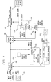
- FIG. 1 shows, in simplified block diagram form, details of a synchronization arrangement including an embodiment of the invention.
- FIG. 1 shows a digital synchronization arrangement including an embodiment of the invention.
- a digital transmission signal to be synchronized to a local output clock signal is supplied from input data source 101 to serial to parallel (S/P) converter 102.
- the incoming data signal can be any one of a number of digital transmission signals having gaps in the data to be supplied to elastic store 103.
- a SONET STS1 signal is assumed which is supplied in bytes, i.e., eight (8) parallel bits to elastic store 103. It will be apparent to those skilled in the art that the incoming data signal could also be supplied in serial bit form to elastic store 103.
- the SONET STS1 signal has a transmission rate of 51.840 Mbits/sec and includes a frame having nine (9) rows of information. Each row includes 90 bytes of information usually comprising 87 bytes of user data preceded by a "gap" having a duration of three (3) byte intervals.
- the gap duration is only two byte intervals.
- the gap duration is four byte intervals.
- the particular row of the incoming SONET STS1 signal designated for stuffing may comprise 87 bytes of user data and a gap of three (3) byte intervals, or 88 bytes of user data and a gap of two (2) byte intervals, or 86 bytes of user data and a gap of four (4) byte intervals.
- SONET Digital Hierarchy - Optical Interface Rates and Formats Specifications
- S/P converter 102 converts the serial input data signal into parallel bytes including eight (8) bits and supplies the bytes to a data input of elastic store 103 and to gap detector and write control unit 104.
- An incoming clock signal is supplied from input clock source 105 to S/P converter 102, divider 106 and smooth clock generator 108.
- the SONET STS1 clock is 51.840 MHz and frame sync is 8 KHz.
- Divider 106 divides the input clock signal by eight (8) to obtain an input byte clock signal of 6.480 MHz.
- the input byte clock signal is supplied to gap detector and write control 104 and, therein, to counter 107.
- Counter 107 is employed to generate the write address for elastic store 103, in well known fashion.
- the write address is supplied to a write (W) input of elastic store 103.
- W write
- Gap detector and write control 104 is employed to detect the gaps in the incoming data signal. This is realized by detecting the particular information in the predetermined gap byte positions. This information will also indicate whether the stuff byte positions include data or non-data. Again, see the ANSI draft standard and Technical Advisory, noted above, regarding details of stuffing in the STS1 signal. Gap detector and write control 104 operates to inhibit counter 107 from advancing the write address for so-called gap bytes and supplies a representation of the number of byte intervals in the gap, i.e., a gap indication, in a row of the STS1 signal to smooth clock generator 108 and, therein, to controllable divider 109.
- the gap indication is a first control signal representative of the duration of the detected gap, i.e., the number of byte intervals in the gap.
- controllable divider 109 is responsive to the gap indication to divide the input clock of 51.840 MHz by 90/88 when the STS 1 signal row has a gap of two (2) byte intervals duration (one gap byte includes user data), by 90/87 when the STS1 signal row has a gap of the usual three (3) byte intervals duration and by 90/86 when the STS1 signal row has a gap of four (4) byte intervals duration (an additional gap byte is stuffed with non-data).
- the smooth clock signal output from controllable divider 109 is supplied to divider 110 which, in this example, divides it by eight (8) to yield a smooth byte clock signal.
- Counter 111 in response to the smooth byte clock signal generates a smooth write address which, in turn, is supplied to phase detector 112. It is important to note that the smooth write address is substantially evenly distributed over the 90 byte row interval and does not include any gaps. That is, for a STS1 signal row including 88 bytes of incoming user data to be supplied to elastic store 103, the corresponding 88 write addresses generated by counter 111 are evenly, i.e., smoothly, distributed over the 90 byte STS1 signal row interval.
- the smooth write addresses supplied to phase detector 112 do not include any gaps which would cause so-called "jumps" in a write-read address separation signal being generated by phase detector 112.
- the write-read address separation signal is a second control signal representative of the offset between the smooth write addresses and the adjusted read addresses.
- an output clock signal is obtained from output clock source 113.
- the output clock signal is also the STS1 signal clock of 51.480 MHz and is supplied to divider 114 and parallel to serial (P/S) converter 115.
- divider 114 divides the output clock signal by eight (8) to generate an output byte clock signal of 6.480 MHz which is supplied to read control 116.
- Read control 116 includes counter 117 for generating an adjusted read address which, in turn, is supplied to a read address (R) input of elastic store 103 and to phase detector 112. Counter 117 is controlled to be inhibited from advancing the read address when gap bytes are to appear in the output data bytes from the data output of elastic store 103.
- 87 bytes of data are normally supplied as an output from elastic store 103 preceded by a gap of three (3) byte intervals duration which is obtained by inhibiting advancing counter 117 to form a STS1 signal row of 90 bytes.
- an additional byte of data is supplied as an output in the STS1 signal row assigned for stuffing. That is, 88 bytes of data are supplied as an output from elastic store 103 preceded by a gap of two (2) byte intervals duration obtained by appropriately inhibiting advancing counter 117 to form the STS1 signal row assigned to stuffing.
- the gap in the adjusted read address will not affect the write-read address separation signal being generated by phase detector 112 at the stuff decision points. This result is attained because the smooth write address will eventually "catch up" to the adjusted read address by the time the stuff decision point is reached and because the write-read address separation signal is not evaluated, i.e., compared to the predetermined threshold values, in making a stuff decision until the stuff decision point is reached.
- the outgoing data bytes from elastic store 103 are supplied to parallel to serial (P/S) converter 115 which yields the desired output data signal at the STS1 signal rate of 51.480 Mbits/s. Since P/S convener 115 is supplied with the 51.480 Mhz output clock signal, a gap will appear in the output data signal having a duration equal to the number of byte intervals that the adjusted read address is inhibited from advancing.
- P/S converter 115 Since P/S convener 115 is supplied with the 51.480 Mhz output clock signal, a gap will appear in the output data signal having a duration equal to the number of byte intervals that the adjusted read address is inhibited from advancing.
Claims (10)
- Vorrichtung zur Synchronisierung eines Eingangsdatensignals mit einem Eingangstaktsignal auf ein neues Ausgangstaktsignal, um ein Ausgangsdatensignal zu ergeben, miteiner Quelle eines Eingangsdatensignals (101);einer Quelle eines Eingangstaktsignals (105);einer Quelle eines Ausgangstaktsignals (113);einem Phasendetektor (112); undmit dem besagten Eingangsdatensignal, Schreibadressen und Leseadressen versorgten elastischen Speichermitteln (103) zum Abgeben von mit dem besagten Ausgangstaktsignal synchronisierten Daten als Ausgabe;gekennzeichnet durchMittel (104) zum Erkennen von mindestens einem Spalt in einem vorbestimmten Teil eines vorbestimmten festen Zeitraums des besagten Eingangsdatensignals und zum Erzeugen eines ersten Steuersignals, das für die Dauer des besagten erkannten mindestens einen Spalts repräsentativ ist;mit dem besagten Eingangstaktsignal versorgte und auf das besagte erste Steuersignal reagierende Mittel (104) zum Erzeugen der besagten Schreibadressen, wobei die besagten Mittel zum Erzeugen der besagten Schreibadressen Mittel (104, 107) zum Sperren des Fortschaltens der besagten Schreibadressen für die Anzahl von Bytezeiten im besagten mindestens einen Spalt enthalten;mit dem besagten Eingangstaktsignal versorgte und auf das erste Steuersignal reagierende Mittel (108-111) zum Erzeugen von gleichmäßigen Schreibadressen, die gleichmäßig über die besagte vorbestimmte feste Zeitdauer des Eingangsdatensignals verteilt sind und zahlenmäßig in Abhängigkeit von der Dauer des erkannten mindestens einen Spalts variiert werden; undmit dem besagten Ausgangstaktsignal versorgte und auf ein zweites Steuersignal reagierende Mittel (116) zum Erzeugen von eingestellten Leseadressen, die dem elastischen Speichermittel (103) als die Leseadressen zugeführt werden, wobei die besagten Mittel zum Erzeugen der besagten eingestellten Leseadressen auf besagtes zweites Steuersignal reagierende Mittel (116) zum Sperren des Fortschaltens der besagten eingestellten Leseadressen für die Dauer von mindestens einem Spalt, der in das besagte Ausgangsdatensignal einzublenden ist, enthalten, wobei die besagten Mittel (116) zum Sperren so gesteuert werden, daß der besagte mindestens eine Spalt in einen vorbestimmten Teil des besagten Ausgangsdatensignals eingeblendet wird, und wobei die besagten Mittel zum Erzeugen der besagten eingestellten Leseadressen Mittel zum Auswerten des besagten zweiten Steuersignals zu vorgeschriebenen Zeitpunkten während eines vorbestimmten Teils des besagten Ausgangsdatensignals enthalten, wobei die besagten Zeitpunkte in einem vorbestimmten Verhältnis dazu stehen, wo der besagte mindestens eine Spalt in den besagten vorbestimmten Teil des besagten Ausgangsdatensignals einzublenden ist;wobei der Phasendetektor (112) mit den besagten gleichmäßigen Schreibadressen und den besagten eingestellten Leseadressen versorgt wird, um das besagte zweite Steuersignal zu erzeugen, das für die Trennung, d.h. den Versatz zwischen den besagten gleichmäßigen Schreibadressen und den besagten eingestellten Leseadressen repräsentativ ist.
- Vorrichtung nach Anspruch 1, wobei die besagten Mittel (108) zum Erzeugen der besagten gleichmäßigen Schreibadressen auf das besagte erste Steuersignal reagierende steuerbare Teilermittel (109) zum Teilen des besagten Eingangstaktsignals um einen im Verhältnis zum besagten vorbestimmten Teil des besagten Eingangsdatensignals und der besagten Dauer des besagten erkannten mindestens einen Spalts stehenden Faktor zum Erhalten eines gleichmäßigen Taktsignals und mit dem besagten gleichmäßigen Taktsignal versorgte Mittel (111) zum Erzeugen der besagten gleichmäßigen Schreibadressen enthalten.
- Vorrichtung nach Anspruch 2, wobei der besagte vorbestimmte Teil des besagten Eingangsdatensignals eine vorbestimmte Gesamtzahl von Byte enthält, die besagte Dauer des besagten mindestens einen Spalts ein oder mehrere Byteintervalle beträgt und der besagte Faktor ein Verhältnis der besagten Gesamtzahl von Byte über die besagte Gesamtzahl von Byte weniger die Anzahl von Byteintervallen im besagten mindestens einen Spalt ist.
- Vorrichtung nach Anspruch 3, wobei die mit dem besagten gleichmäßigen Taktsignal versorgten besagten Mittel Mittel (110) zum Teilen des besagten gleichmäßigen Taktsignals durch eine vorbestimmte Nummer zum Erhalten eines gleichmäßigen Bytetaktsignals und mit dem besagten gleichmäßigen Bytetaktsignal versorgte Zählermittel (111) zum Erzeugen der besagten gleichmäßigen Schreibadressen enthalten.
- Vorrichtung nach Anspruch 2, wobei der besagte erkannte mindestens eine Spalt eine Dauer von einem oder mehreren Byteintervallen aufweist, die besagten Mittel zum Erzeugen der besagten Schreibadressen Mittel (106) zum Teilen des besagten Eingangstaktsignals durch eine vorbestimmte Nummer zum Erhalten eines Eingangsbytetaktsignals und mit dem besagten Eingangsbytetaktsignal versorgte Zählermittel (107) zum Erzeugen der besagten Schreibadressen enthalten, und besagte Mittel (104) zum Sperren das Fortschalten der besagten Zählermittel für die besagte Dauer des besagten erkannten mindestens einen Spalts sperren.
- Vorrichtung nach Anspruch 5, wobei der in das besagte Ausgangsdatensignal einzublendende besagte mindestens eine Spalt eine Dauer von einem oder mehreren Byteintervallen aufweist, die besagten Mittel (116) zum Erzeugen der besagten eingestellten Leseadressen Mittel (114) zum Teilen des besagten Ausgangstaktsignals zum Erhalten eines Ausgangsbytetaktsignals und mit dem besagten Ausgangsbytetaktsignal versorgte Zählermittel (117) zum Erzeugen der besagten eingestellten Leseadressen enthalten, und besagte Mittel (116) zum Sperren das Fortschalten der besagten Zählermittel (117) für die besagte Dauer von mindestens einem in das besagte Ausgangsdatensignal einzublendenden Spalt sperren.
- Vorrichtung nach Anspruch 6, wobei das Eingangsdatensignal eine serielle Form aufweist und Serien-Parallelwandlermittel (102) zum Umwandeln des besagten Eingangsdatensignals von serieller Form in parallele Byte, die als Eingabe in das besagte elastische Speichermittel (103) abgegeben werden, bereitgestellt werden.
- Vorrichtung nach Anspruch 7, wobei das besagte Ausgangsdatensignal in paralleler Byteform aus dem elastischen Speichermittel (103) ausgelesen wird und Parallel-Serienwandlermittel (115) zum Umwandeln der parallelen Byte des aus dem besagten elastischen Speichermittel (103) ausgelesenen Ausgangsdatensignals in Serienform bereitgestellt werden.
- Vorrichtung nach Anspruch 6, wobei das besagte Eingangsdatensignal ein SONET-STS1-Signal ist, das besagte vorbestimmte feste Intervall des besagten Eingangsdatensignals eine STS1-Signalzeile mit 90 Byte ist und das besagte Eingangstaktsignal ein STS1-Taktsignal ist.
- Vorrichtung nach Anspruch 9, wobei das besagte Ausgangsdatensignal ein SONET-STS1-Signal ist, das besagte vorbestimmte feste Intervall des besagten Ausgangsdatensignals eine STS1-Signalzeile mit 90 Byte ist und das besagte Ausgangstaktsignal ein STS1-Taktsignal ist.
Applications Claiming Priority (2)
| Application Number | Priority Date | Filing Date | Title |
|---|---|---|---|
| US07/530,774 US5119406A (en) | 1990-05-30 | 1990-05-30 | Digital signal synchronization employing single elastic store |
| US530774 | 1990-05-30 |
Publications (3)
| Publication Number | Publication Date |
|---|---|
| EP0459686A2 EP0459686A2 (de) | 1991-12-04 |
| EP0459686A3 EP0459686A3 (en) | 1992-08-26 |
| EP0459686B1 true EP0459686B1 (de) | 1996-12-27 |
Family
ID=24114909
Family Applications (1)
| Application Number | Title | Priority Date | Filing Date |
|---|---|---|---|
| EP91304591A Expired - Lifetime EP0459686B1 (de) | 1990-05-30 | 1991-05-21 | Synchronisierung eines digitalen Signals mit einer elastischen Speicherung |
Country Status (6)
| Country | Link |
|---|---|
| US (1) | US5119406A (de) |
| EP (1) | EP0459686B1 (de) |
| JP (1) | JP2563691B2 (de) |
| KR (1) | KR0175662B1 (de) |
| CA (1) | CA2036162C (de) |
| DE (1) | DE69123785T2 (de) |
Families Citing this family (40)
| Publication number | Priority date | Publication date | Assignee | Title |
|---|---|---|---|---|
| EP0409861A1 (de) * | 1989-02-16 | 1991-01-30 | International Business Machines Corporation | Asynchroner datenkanal für informationsspeicher-untersysteme |
| DE4027967A1 (de) * | 1990-09-04 | 1992-03-05 | Philips Patentverwaltung | Stopfentscheidungsschaltung fuer eine anordnung zur bitratenanpassung |
| JP2600496B2 (ja) * | 1990-12-20 | 1997-04-16 | 日本電気株式会社 | セル位相乗換回路 |
| US5638411A (en) * | 1991-05-23 | 1997-06-10 | Mitsubishi Denki Kabushiki Kaisha | Stuff bit synchronization system |
| US5268936A (en) * | 1991-07-08 | 1993-12-07 | At&T Bell Laboratories | Synchronous digital signal to asynchronous digital signal desynchronizer |
| US5268935A (en) * | 1991-12-20 | 1993-12-07 | At&T Bell Laboratories | Synchronous digital signal to asynchronous digital signal desynchronizer |
| ES2046106B1 (es) * | 1992-02-18 | 1996-11-16 | Estandard Electrica S A | Metodo de realizacion de circuitos alineadores inmunes a los deslizamientos ocurridos en la memoria elastica de recepcion. |
| JP2888022B2 (ja) * | 1992-04-02 | 1999-05-10 | 三菱電機株式会社 | 通信制御装置 |
| US5717693A (en) * | 1992-05-21 | 1998-02-10 | Alcatel Network Systems, Inc. | Sonet payload pointer processing and architecture |
| DE69324522T2 (de) * | 1992-05-27 | 1999-09-16 | Ericsson Telefon Ab L M | Verfahren und Anordnung zur Anpassung der Geschwindigkeit des Auslesens von Daten aus einem Speicher an die Geschwindigkeit des Einschreibens von Daten in den Speicher |
| EP0578315A1 (de) * | 1992-07-09 | 1994-01-12 | Philips Patentverwaltung GmbH | Synchrones Übertragungssystem |
| US5885489A (en) * | 1992-11-03 | 1999-03-23 | Eta Process Plant Limited | Packing elements |
| CH686465A5 (de) * | 1993-01-26 | 1996-03-29 | Royale Consultants Ltd | Verfahren und Einrichtung zur bidirektionalen Informationsuebertragung (Full-Duplex). |
| FI94812C (fi) * | 1993-05-18 | 1995-10-25 | Nokia Telecommunications Oy | Menetelmä ja laite tasauspäätöksen aikaansaamiseksi synkronisen digitaalisen tietoliikennejärjestelmän solmupisteessä |
| US5457717A (en) * | 1993-11-29 | 1995-10-10 | Dsc Communications Corporation | Apparatus and method for eliminating mapping jitter |
| US5548534A (en) * | 1994-07-08 | 1996-08-20 | Transwitch Corporation | Two stage clock dejitter circuit for regenerating an E4 telecommunications signal from the data component of an STS-3C signal |
| KR0177733B1 (ko) * | 1994-08-26 | 1999-05-15 | 정장호 | 데이타 전송장치의 클럭동기 회로 |
| JP3408652B2 (ja) * | 1995-02-03 | 2003-05-19 | 沖電気工業株式会社 | ビット位相同期回路 |
| US5583894A (en) * | 1995-03-20 | 1996-12-10 | Vlsi Technology, Inc. | Slip buffer for synchronizing data transfer between two devices |
| US5699391A (en) * | 1995-05-31 | 1997-12-16 | Dsc Communications Corporation | Digital desynchronizer |
| US5761203A (en) * | 1996-04-04 | 1998-06-02 | Lucent Technologies Inc. | Synchronous and asynchronous recovery of signals in an ATM network |
| GB2312353B (en) * | 1996-04-16 | 2000-12-06 | Gpt Ltd | Digital telecommunications transmision systems |
| US6064706A (en) * | 1996-05-01 | 2000-05-16 | Alcatel Usa, Inc. | Apparatus and method of desynchronizing synchronously mapped asynchronous data |
| JPH10210503A (ja) * | 1997-01-17 | 1998-08-07 | Sony Corp | 信号変換装置 |
| US5990713A (en) * | 1998-02-05 | 1999-11-23 | Harris Corporation | Adjustable phase clock circuit using the same and related methods |
| EP0935362A3 (de) * | 1998-02-06 | 2005-02-02 | Alcatel | Synchronisiereinrichtung für ein synchrones digitales Nachrichtenübertragungssystem und Verfahren zum Erzeugen eines synchronen Ausgangssignales |
| CA2327484C (en) * | 1998-04-07 | 2008-05-20 | Siemens Aktiengesellschaft | Method and apparatus for coupling an atm communication layer to a plurality of time-division multiplex communication terminals |
| US6289066B1 (en) * | 1998-06-11 | 2001-09-11 | Hewlett-Packard Company | Method and apparatus for recentering an elasticity FIFO when receiving 1000BASE-X traffic using minimal information |
| US6501809B1 (en) * | 1999-03-19 | 2002-12-31 | Conexant Systems, Inc. | Producing smoothed clock and data signals from gapped clock and data signals |
| JP3419345B2 (ja) * | 1999-05-28 | 2003-06-23 | 日本電気株式会社 | パルススタッフ同期方式における低次群信号のクロック再生方法および回路 |
| US6956873B2 (en) * | 2001-05-21 | 2005-10-18 | General Instrument Corporation | Arrangement for deriving a local clock in a packet cable telephony modem |
| US6882662B2 (en) * | 2001-06-07 | 2005-04-19 | Applied Micro Circuits Corporation | Pointer adjustment wander and jitter reduction apparatus for a desynchronizer |
| KR100443014B1 (ko) * | 2001-12-24 | 2004-08-04 | 엘지전자 주식회사 | 듀얼포트램을 이용한 상이위상 클럭간 데이터 전송 장치 |
| US7606269B1 (en) * | 2004-07-27 | 2009-10-20 | Intel Corporation | Method and apparatus for detecting and managing loss of alignment in a virtually concatenated group |
| US8867682B2 (en) * | 2010-08-30 | 2014-10-21 | Exar Corporation | Dejitter (desynchronize) technique to smooth gapped clock with jitter/wander attenuation using all digital logic |
| US8855258B1 (en) | 2011-04-20 | 2014-10-07 | Applied Micro Circuits Corporation | Transmitters and receivers using a jitter-attenuated clock derived from a gapped clock reference |
| US8666011B1 (en) | 2011-04-20 | 2014-03-04 | Applied Micro Circuits Corporation | Jitter-attenuated clock using a gapped clock reference |
| US9673963B1 (en) * | 2016-04-12 | 2017-06-06 | Keyssa Systems, Inc. | Multi-protocols and multi-data rates communications |
| US10056890B2 (en) | 2016-06-24 | 2018-08-21 | Exar Corporation | Digital controlled oscillator based clock generator for multi-channel design |
| US10063365B1 (en) | 2017-03-10 | 2018-08-28 | Keyssa Systems, Inc. | Re-timer network insertion |
Family Cites Families (6)
| Publication number | Priority date | Publication date | Assignee | Title |
|---|---|---|---|---|
| GB1532444A (en) * | 1975-03-26 | 1978-11-15 | Micro Consultants Ltd | Synchronising data for digital storage systems |
| US4347620A (en) * | 1980-09-16 | 1982-08-31 | Northern Telecom Limited | Method of and apparatus for regenerating a signal frequency in a digital signal transmission system |
| JPS61281635A (ja) * | 1985-05-29 | 1986-12-12 | Kenwood Corp | 時分割多重信号分離方式 |
| CA1262173A (en) * | 1986-05-29 | 1989-10-03 | James Angus Mceachern | Synchronization of asynchronous data signals |
| US4928275A (en) * | 1989-05-26 | 1990-05-22 | Northern Telecom Limited | Synchronization of asynchronous data signals |
| DE3942885A1 (de) * | 1989-12-23 | 1991-06-27 | Philips Patentverwaltung | Schaltungsanordnung zur bitratenanpassung |
-
1990
- 1990-05-30 US US07/530,774 patent/US5119406A/en not_active Expired - Lifetime
-
1991
- 1991-02-12 CA CA002036162A patent/CA2036162C/en not_active Expired - Fee Related
- 1991-05-21 JP JP3144144A patent/JP2563691B2/ja not_active Expired - Fee Related
- 1991-05-21 DE DE69123785T patent/DE69123785T2/de not_active Expired - Fee Related
- 1991-05-21 EP EP91304591A patent/EP0459686B1/de not_active Expired - Lifetime
- 1991-05-23 KR KR1019910008294A patent/KR0175662B1/ko not_active IP Right Cessation
Also Published As
| Publication number | Publication date |
|---|---|
| JPH04233348A (ja) | 1992-08-21 |
| CA2036162A1 (en) | 1991-12-01 |
| DE69123785D1 (de) | 1997-02-06 |
| DE69123785T2 (de) | 1997-04-17 |
| EP0459686A2 (de) | 1991-12-04 |
| KR910021068A (ko) | 1991-12-20 |
| EP0459686A3 (en) | 1992-08-26 |
| JP2563691B2 (ja) | 1996-12-11 |
| KR0175662B1 (ko) | 1999-05-15 |
| CA2036162C (en) | 1995-02-21 |
| US5119406A (en) | 1992-06-02 |
Similar Documents
| Publication | Publication Date | Title |
|---|---|---|
| EP0459686B1 (de) | Synchronisierung eines digitalen Signals mit einer elastischen Speicherung | |
| EP0473338B1 (de) | Bitsynchronisierung mittels elastisches Speichers | |
| US5268935A (en) | Synchronous digital signal to asynchronous digital signal desynchronizer | |
| US4996698A (en) | Clock signal resynchronizing apparatus | |
| US4928275A (en) | Synchronization of asynchronous data signals | |
| US6229863B1 (en) | Reducing waiting time jitter | |
| US5263057A (en) | Method of reducing waiting time jitter | |
| US5255293A (en) | Phase locked loop arrangement | |
| US4095053A (en) | Quasi-pulse stuffing synchronization | |
| US5276688A (en) | Circuit arrangement for bit rate adjustment | |
| EP0630127B1 (de) | Anordnung von digitalen Phasenregelschleifen | |
| EP0500243B1 (de) | Verteilte Bit für Bit Entstopfungsschaltung für bytegestopfte Mehrfachrahmendaten | |
| US4847875A (en) | Timing circuit including jitter compensation | |
| EP0584636B1 (de) | Phasendetektor für elastischen Speicherung | |
| US7212599B2 (en) | Jitter and wander reduction apparatus | |
| JPH11266221A (ja) | ペイロード相対位置変更要求装置及びそれを含む伝送装置 | |
| GB2387092A (en) | Switching between clocks to read a buffer in a data receiving circuit | |
| JPH0621929A (ja) | 伝送装置および等化回路装置 | |
| US5548624A (en) | Destuff circuit for asynchronous digital signals | |
| JP2697371B2 (ja) | スタッフ多重通信受信回路 | |
| US7058073B2 (en) | Arrangement and method for transmitting data over a TDM bus | |
| JP2952935B2 (ja) | 非同期データ伝送システム | |
| EP1034632B1 (de) | Verfahren zur übertragung von datensignalen sowie verfahren und vorrichtung zur desynchronisierung von pdh signalen | |
| KR100338696B1 (ko) | 동기화 시스템 | |
| JP3010634B2 (ja) | フレーム同期多重処理方式 |
Legal Events
| Date | Code | Title | Description |
|---|---|---|---|
| PUAI | Public reference made under article 153(3) epc to a published international application that has entered the european phase |
Free format text: ORIGINAL CODE: 0009012 |
|
| AK | Designated contracting states |
Kind code of ref document: A2 Designated state(s): BE DE FR GB IT NL SE |
|
| PUAL | Search report despatched |
Free format text: ORIGINAL CODE: 0009013 |
|
| AK | Designated contracting states |
Kind code of ref document: A3 Designated state(s): BE DE FR GB IT NL SE |
|
| 17P | Request for examination filed |
Effective date: 19930211 |
|
| RAP3 | Party data changed (applicant data changed or rights of an application transferred) |
Owner name: AT&T CORP. |
|
| 17Q | First examination report despatched |
Effective date: 19950905 |
|
| GRAG | Despatch of communication of intention to grant |
Free format text: ORIGINAL CODE: EPIDOS AGRA |
|
| GRAH | Despatch of communication of intention to grant a patent |
Free format text: ORIGINAL CODE: EPIDOS IGRA |
|
| GRAH | Despatch of communication of intention to grant a patent |
Free format text: ORIGINAL CODE: EPIDOS IGRA |
|
| GRAA | (expected) grant |
Free format text: ORIGINAL CODE: 0009210 |
|
| AK | Designated contracting states |
Kind code of ref document: B1 Designated state(s): BE DE FR GB IT NL SE |
|
| ITF | It: translation for a ep patent filed |
Owner name: JACOBACCI & PERANI S.P.A. |
|
| ET | Fr: translation filed | ||
| REF | Corresponds to: |
Ref document number: 69123785 Country of ref document: DE Date of ref document: 19970206 |
|
| PLBE | No opposition filed within time limit |
Free format text: ORIGINAL CODE: 0009261 |
|
| STAA | Information on the status of an ep patent application or granted ep patent |
Free format text: STATUS: NO OPPOSITION FILED WITHIN TIME LIMIT |
|
| 26N | No opposition filed | ||
| PGFP | Annual fee paid to national office [announced via postgrant information from national office to epo] |
Ref country code: BE Payment date: 19990329 Year of fee payment: 9 |
|
| PG25 | Lapsed in a contracting state [announced via postgrant information from national office to epo] |
Ref country code: BE Free format text: LAPSE BECAUSE OF NON-PAYMENT OF DUE FEES Effective date: 20000531 |
|
| BERE | Be: lapsed |
Owner name: AT&T CORP. Effective date: 20000531 |
|
| REG | Reference to a national code |
Ref country code: GB Ref legal event code: IF02 |
|
| PGFP | Annual fee paid to national office [announced via postgrant information from national office to epo] |
Ref country code: NL Payment date: 20090527 Year of fee payment: 19 |
|
| PGFP | Annual fee paid to national office [announced via postgrant information from national office to epo] |
Ref country code: SE Payment date: 20090514 Year of fee payment: 19 Ref country code: IT Payment date: 20090527 Year of fee payment: 19 Ref country code: DE Payment date: 20090525 Year of fee payment: 19 Ref country code: FR Payment date: 20090513 Year of fee payment: 19 |
|
| PGFP | Annual fee paid to national office [announced via postgrant information from national office to epo] |
Ref country code: GB Payment date: 20090522 Year of fee payment: 19 |
|
| REG | Reference to a national code |
Ref country code: NL Ref legal event code: V1 Effective date: 20101201 |
|
| GBPC | Gb: european patent ceased through non-payment of renewal fee |
Effective date: 20100521 |
|
| EUG | Se: european patent has lapsed | ||
| REG | Reference to a national code |
Ref country code: FR Ref legal event code: ST Effective date: 20110131 |
|
| PG25 | Lapsed in a contracting state [announced via postgrant information from national office to epo] |
Ref country code: NL Free format text: LAPSE BECAUSE OF NON-PAYMENT OF DUE FEES Effective date: 20101201 Ref country code: SE Free format text: LAPSE BECAUSE OF NON-PAYMENT OF DUE FEES Effective date: 20100522 Ref country code: IT Free format text: LAPSE BECAUSE OF NON-PAYMENT OF DUE FEES Effective date: 20100521 |
|
| PG25 | Lapsed in a contracting state [announced via postgrant information from national office to epo] |
Ref country code: DE Free format text: LAPSE BECAUSE OF NON-PAYMENT OF DUE FEES Effective date: 20101201 |
|
| PG25 | Lapsed in a contracting state [announced via postgrant information from national office to epo] |
Ref country code: FR Free format text: LAPSE BECAUSE OF NON-PAYMENT OF DUE FEES Effective date: 20100531 |
|
| PG25 | Lapsed in a contracting state [announced via postgrant information from national office to epo] |
Ref country code: GB Free format text: LAPSE BECAUSE OF NON-PAYMENT OF DUE FEES Effective date: 20100521 |