EP0457622A2 - Verstärker mit variabler Verstärkung - Google Patents
Verstärker mit variabler Verstärkung Download PDFInfo
- Publication number
- EP0457622A2 EP0457622A2 EP91304495A EP91304495A EP0457622A2 EP 0457622 A2 EP0457622 A2 EP 0457622A2 EP 91304495 A EP91304495 A EP 91304495A EP 91304495 A EP91304495 A EP 91304495A EP 0457622 A2 EP0457622 A2 EP 0457622A2
- Authority
- EP
- European Patent Office
- Prior art keywords
- level
- gain
- resistor
- amplifier
- whose
- Prior art date
- Legal status (The legal status is an assumption and is not a legal conclusion. Google has not performed a legal analysis and makes no representation as to the accuracy of the status listed.)
- Granted
Links
Images


Classifications
-
- H—ELECTRICITY
- H03—ELECTRONIC CIRCUITRY
- H03G—CONTROL OF AMPLIFICATION
- H03G3/00—Gain control in amplifiers or frequency changers
- H03G3/02—Manually-operated control
- H03G3/04—Manually-operated control in untuned amplifiers
- H03G3/10—Manually-operated control in untuned amplifiers having semiconductor devices
-
- H—ELECTRICITY
- H03—ELECTRONIC CIRCUITRY
- H03G—CONTROL OF AMPLIFICATION
- H03G1/00—Details of arrangements for controlling amplification
- H03G1/0005—Circuits characterised by the type of controlling devices operated by a controlling current or voltage signal
- H03G1/0017—Circuits characterised by the type of controlling devices operated by a controlling current or voltage signal the device being at least one of the amplifying solid-state elements
- H03G1/0023—Circuits characterised by the type of controlling devices operated by a controlling current or voltage signal the device being at least one of the amplifying solid-state elements in emitter-coupled or cascode amplifiers
Definitions
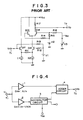
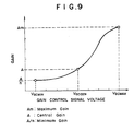
- an attenuation ratio of the attenuator circuit 5 with respect to an input is set to "1" when a level of the gain control signal V GC is the maximum, is set to 1/n at a central voltage value, and is set to "0" at the minimum value.
- the conventional variable gain amplifier described above has a following disadvantage. That is, the level controlling range of the gain control signal V GC is not of a symmetrical characteristic with respect to the central value (V GCCEN ) of the gain control signal V GC if an attempt is made on setting the gain controllable range among A/n times ⁇ A times ⁇ nA times. This is because such conventional variable gain amplifier is so arranged that the minimum value of the gain becomes "0" when the gain control signal V GC is rendered to the minimum value.
- a resistance ratio between the resistor R2 and the resistor R3 should be set to 1 : 2
- a resistance ratio between the resistor R4 and the resistor R3 should be set to 2 : 3
- the emitter area ratio between the transistors Q4 and Q5 should be set to 1 : 2.
- both the transistors Q24 and Q25 turn ON and each transistor has a signal distribution passing ratio according to the emitter area ratio between both the transistors, that is, 4 : 1, the signal output of the second amplifier circuit 22 having the gain of 2.5 times and formed by the resistor R21, the transistor Q23 and the resistor R23 is multiplied by 0.5 times and then outputted to the terminal T26 as a signal corresponding to 0.5 times.
Landscapes
- Control Of Amplification And Gain Control (AREA)
Applications Claiming Priority (2)
| Application Number | Priority Date | Filing Date | Title |
|---|---|---|---|
| JP2129832A JP2690599B2 (ja) | 1990-05-18 | 1990-05-18 | 可変利得増幅器 |
| JP129832/90 | 1990-05-18 |
Publications (3)
| Publication Number | Publication Date |
|---|---|
| EP0457622A2 true EP0457622A2 (de) | 1991-11-21 |
| EP0457622A3 EP0457622A3 (en) | 1992-02-26 |
| EP0457622B1 EP0457622B1 (de) | 1995-07-26 |
Family
ID=15019336
Family Applications (1)
| Application Number | Title | Priority Date | Filing Date |
|---|---|---|---|
| EP91304495A Expired - Lifetime EP0457622B1 (de) | 1990-05-18 | 1991-05-20 | Verstärker mit variabler Verstärkung |
Country Status (4)
| Country | Link |
|---|---|
| US (1) | US5113149A (de) |
| EP (1) | EP0457622B1 (de) |
| JP (1) | JP2690599B2 (de) |
| DE (1) | DE69111510T2 (de) |
Families Citing this family (5)
| Publication number | Priority date | Publication date | Assignee | Title |
|---|---|---|---|---|
| US5717360A (en) * | 1996-04-16 | 1998-02-10 | National Semiconductor Corporation | High speed variable gain amplifier |
| JPH11330876A (ja) | 1998-05-15 | 1999-11-30 | Nec Corp | 電圧制御増幅回路 |
| US6031421A (en) * | 1998-07-22 | 2000-02-29 | Mcewan; Thomas E. | Controlled gain amplifier with variable control exponent |
| US7260377B2 (en) * | 2002-12-02 | 2007-08-21 | Broadcom Corporation | Variable-gain low noise amplifier for digital terrestrial applications |
| JP4683866B2 (ja) * | 2004-06-18 | 2011-05-18 | アピックヤマダ株式会社 | 半導体装置の製造装置 |
Family Cites Families (4)
| Publication number | Priority date | Publication date | Assignee | Title |
|---|---|---|---|---|
| DE2350643A1 (de) * | 1973-10-09 | 1975-04-10 | Braun Ag | Aussteuerungsautomatik fuer tonbandgeraete |
| JPS5646312A (en) * | 1979-09-21 | 1981-04-27 | Toshiba Corp | Variable gain circuit |
| JPS58196709A (ja) * | 1982-05-12 | 1983-11-16 | Mitsubishi Electric Corp | 電子制御選択増幅回路 |
| JPS6051309A (ja) * | 1983-08-31 | 1985-03-22 | Toshiba Corp | 利得制御回路 |
-
1990
- 1990-05-18 JP JP2129832A patent/JP2690599B2/ja not_active Expired - Fee Related
-
1991
- 1991-05-17 US US07/702,628 patent/US5113149A/en not_active Expired - Fee Related
- 1991-05-20 DE DE69111510T patent/DE69111510T2/de not_active Expired - Fee Related
- 1991-05-20 EP EP91304495A patent/EP0457622B1/de not_active Expired - Lifetime
Also Published As
| Publication number | Publication date |
|---|---|
| US5113149A (en) | 1992-05-12 |
| JP2690599B2 (ja) | 1997-12-10 |
| EP0457622B1 (de) | 1995-07-26 |
| EP0457622A3 (en) | 1992-02-26 |
| DE69111510D1 (de) | 1995-08-31 |
| DE69111510T2 (de) | 1995-12-21 |
| JPH0425209A (ja) | 1992-01-29 |
Similar Documents
| Publication | Publication Date | Title |
|---|---|---|
| EP0938188B1 (de) | Verstärker mit variabler Verstärkung | |
| EP0004099B1 (de) | Elektrisch einstellbare Impedanzschaltung | |
| EP0505751B1 (de) | Logaritmische Verstärkungsschaltung | |
| US3924199A (en) | N-pole filter circuit having cascaded filter sections | |
| EP0196906A2 (de) | Schaltung zur Detektion eines automatischen Verstärkungsregelungssignals | |
| JPH0738554B2 (ja) | 対数増幅器 | |
| EP0457622B1 (de) | Verstärker mit variabler Verstärkung | |
| US4473780A (en) | Amplifier circuit and focus voltage supply circuit incorporating such an amplifier circuit | |
| EP0052117B1 (de) | Biquadratisches aktives filter im strom-modus | |
| EP0834986B1 (de) | Verstärkungsregelungsschaltung und Verstärkungsregelungsverfahren | |
| US3962650A (en) | Integrated circuit amplifier having controlled gain and stable quiescent output voltage level | |
| US5463309A (en) | Variable voltage to current conversion circuit | |
| EP1084532A1 (de) | Linearer in der verstärkung veränderbarer vier-transistor und verfahren zu seinem aufbau | |
| US4434380A (en) | Compensation for VCA OP amp errors | |
| JP3451850B2 (ja) | ミキサ回路 | |
| US4038566A (en) | Multiplier circuit | |
| US4661780A (en) | Differential stage particularly for active filters | |
| US4456886A (en) | Control circuit for voltage controlled variable attenuator | |
| JP3093687B2 (ja) | 利得可変増幅回路 | |
| EP0178936A2 (de) | Variable Anhebungsschaltung | |
| CA1147819A (en) | Gain control systems | |
| JPH10256852A (ja) | 可変伝達コンダクタンス増幅装置 | |
| JPH0514078A (ja) | 電圧制御増幅器 | |
| JPH0344454B2 (de) | ||
| US4311873A (en) | Bias control circuit and method for use in audio reproduction system or the like |
Legal Events
| Date | Code | Title | Description |
|---|---|---|---|
| PUAI | Public reference made under article 153(3) epc to a published international application that has entered the european phase |
Free format text: ORIGINAL CODE: 0009012 |
|
| 17P | Request for examination filed |
Effective date: 19910530 |
|
| AK | Designated contracting states |
Kind code of ref document: A2 Designated state(s): DE FR GB |
|
| PUAL | Search report despatched |
Free format text: ORIGINAL CODE: 0009013 |
|
| AK | Designated contracting states |
Kind code of ref document: A3 Designated state(s): DE FR GB |
|
| 17Q | First examination report despatched |
Effective date: 19940718 |
|
| GRAA | (expected) grant |
Free format text: ORIGINAL CODE: 0009210 |
|
| AK | Designated contracting states |
Kind code of ref document: B1 Designated state(s): DE FR GB |
|
| REF | Corresponds to: |
Ref document number: 69111510 Country of ref document: DE Date of ref document: 19950831 |
|
| ET | Fr: translation filed | ||
| PLBE | No opposition filed within time limit |
Free format text: ORIGINAL CODE: 0009261 |
|
| STAA | Information on the status of an ep patent application or granted ep patent |
Free format text: STATUS: NO OPPOSITION FILED WITHIN TIME LIMIT |
|
| 26N | No opposition filed | ||
| REG | Reference to a national code |
Ref country code: GB Ref legal event code: IF02 |
|
| REG | Reference to a national code |
Ref country code: GB Ref legal event code: 732E |
|
| PGFP | Annual fee paid to national office [announced via postgrant information from national office to epo] |
Ref country code: FR Payment date: 20030508 Year of fee payment: 13 |
|
| PGFP | Annual fee paid to national office [announced via postgrant information from national office to epo] |
Ref country code: GB Payment date: 20030514 Year of fee payment: 13 |
|
| PGFP | Annual fee paid to national office [announced via postgrant information from national office to epo] |
Ref country code: DE Payment date: 20030529 Year of fee payment: 13 |
|
| REG | Reference to a national code |
Ref country code: FR Ref legal event code: TP |
|
| PG25 | Lapsed in a contracting state [announced via postgrant information from national office to epo] |
Ref country code: GB Free format text: LAPSE BECAUSE OF NON-PAYMENT OF DUE FEES Effective date: 20040520 |
|
| PG25 | Lapsed in a contracting state [announced via postgrant information from national office to epo] |
Ref country code: DE Free format text: LAPSE BECAUSE OF NON-PAYMENT OF DUE FEES Effective date: 20041201 |
|
| GBPC | Gb: european patent ceased through non-payment of renewal fee |
Effective date: 20040520 |
|
| PG25 | Lapsed in a contracting state [announced via postgrant information from national office to epo] |
Ref country code: FR Free format text: LAPSE BECAUSE OF NON-PAYMENT OF DUE FEES Effective date: 20050131 |
|
| REG | Reference to a national code |
Ref country code: FR Ref legal event code: ST |