EP0449564B1 - Verfahren für die Reparatur von Leiterbahn-Verbindungen - Google Patents
Verfahren für die Reparatur von Leiterbahn-Verbindungen Download PDFInfo
- Publication number
- EP0449564B1 EP0449564B1 EP91302601A EP91302601A EP0449564B1 EP 0449564 B1 EP0449564 B1 EP 0449564B1 EP 91302601 A EP91302601 A EP 91302601A EP 91302601 A EP91302601 A EP 91302601A EP 0449564 B1 EP0449564 B1 EP 0449564B1
- Authority
- EP
- European Patent Office
- Prior art keywords
- adhesive
- porous sheet
- circuit
- circuits
- substrate
- Prior art date
- Legal status (The legal status is an assumption and is not a legal conclusion. Google has not performed a legal analysis and makes no representation as to the accuracy of the status listed.)
- Expired - Lifetime
Links
- 238000000034 method Methods 0.000 title claims description 20
- 230000008569 process Effects 0.000 title claims description 16
- 239000000853 adhesive Substances 0.000 claims description 78
- 230000001070 adhesive effect Effects 0.000 claims description 78
- 239000000758 substrate Substances 0.000 claims description 33
- 239000007788 liquid Substances 0.000 claims description 30
- 239000011248 coating agent Substances 0.000 claims description 5
- 238000000576 coating method Methods 0.000 claims description 5
- 238000004140 cleaning Methods 0.000 claims description 2
- 230000036961 partial effect Effects 0.000 claims description 2
- 239000002245 particle Substances 0.000 description 10
- 239000011521 glass Substances 0.000 description 8
- 239000011148 porous material Substances 0.000 description 8
- OKKJLVBELUTLKV-UHFFFAOYSA-N Methanol Chemical compound OC OKKJLVBELUTLKV-UHFFFAOYSA-N 0.000 description 6
- -1 polytetrafluoroethylene Polymers 0.000 description 6
- 239000004698 Polyethylene Substances 0.000 description 4
- BDAGIHXWWSANSR-UHFFFAOYSA-N methanoic acid Natural products OC=O BDAGIHXWWSANSR-UHFFFAOYSA-N 0.000 description 4
- 229920000573 polyethylene Polymers 0.000 description 4
- 229920005989 resin Polymers 0.000 description 4
- 239000011347 resin Substances 0.000 description 4
- QTBSBXVTEAMEQO-UHFFFAOYSA-N Acetic acid Chemical compound CC(O)=O QTBSBXVTEAMEQO-UHFFFAOYSA-N 0.000 description 3
- 239000004925 Acrylic resin Substances 0.000 description 3
- 229920000178 Acrylic resin Polymers 0.000 description 3
- YMWUJEATGCHHMB-UHFFFAOYSA-N Dichloromethane Chemical compound ClCCl YMWUJEATGCHHMB-UHFFFAOYSA-N 0.000 description 3
- KWYUFKZDYYNOTN-UHFFFAOYSA-M Potassium hydroxide Chemical compound [OH-].[K+] KWYUFKZDYYNOTN-UHFFFAOYSA-M 0.000 description 3
- HEMHJVSKTPXQMS-UHFFFAOYSA-M Sodium hydroxide Chemical compound [OH-].[Na+] HEMHJVSKTPXQMS-UHFFFAOYSA-M 0.000 description 3
- YXFVVABEGXRONW-UHFFFAOYSA-N Toluene Chemical compound CC1=CC=CC=C1 YXFVVABEGXRONW-UHFFFAOYSA-N 0.000 description 3
- 239000004020 conductor Substances 0.000 description 3
- 230000008595 infiltration Effects 0.000 description 3
- 238000001764 infiltration Methods 0.000 description 3
- 239000000463 material Substances 0.000 description 3
- 230000008439 repair process Effects 0.000 description 3
- 239000002904 solvent Substances 0.000 description 3
- 229920005992 thermoplastic resin Polymers 0.000 description 3
- OSWFIVFLDKOXQC-UHFFFAOYSA-N 4-(3-methoxyphenyl)aniline Chemical compound COC1=CC=CC(C=2C=CC(N)=CC=2)=C1 OSWFIVFLDKOXQC-UHFFFAOYSA-N 0.000 description 2
- ZAKOWWREFLAJOT-CEFNRUSXSA-N D-alpha-tocopherylacetate Chemical compound CC(=O)OC1=C(C)C(C)=C2O[C@@](CCC[C@H](C)CCC[C@H](C)CCCC(C)C)(C)CCC2=C1C ZAKOWWREFLAJOT-CEFNRUSXSA-N 0.000 description 2
- PEDCQBHIVMGVHV-UHFFFAOYSA-N Glycerine Chemical compound OCC(O)CO PEDCQBHIVMGVHV-UHFFFAOYSA-N 0.000 description 2
- VEXZGXHMUGYJMC-UHFFFAOYSA-N Hydrochloric acid Chemical compound Cl VEXZGXHMUGYJMC-UHFFFAOYSA-N 0.000 description 2
- QAOWNCQODCNURD-UHFFFAOYSA-N Sulfuric acid Chemical compound OS(O)(=O)=O QAOWNCQODCNURD-UHFFFAOYSA-N 0.000 description 2
- 239000012790 adhesive layer Substances 0.000 description 2
- 238000007796 conventional method Methods 0.000 description 2
- 239000004744 fabric Substances 0.000 description 2
- 235000019253 formic acid Nutrition 0.000 description 2
- 238000010438 heat treatment Methods 0.000 description 2
- 230000000873 masking effect Effects 0.000 description 2
- 238000002844 melting Methods 0.000 description 2
- 230000009467 reduction Effects 0.000 description 2
- 239000004593 Epoxy Substances 0.000 description 1
- JOYRKODLDBILNP-UHFFFAOYSA-N Ethyl urethane Chemical compound CCOC(N)=O JOYRKODLDBILNP-UHFFFAOYSA-N 0.000 description 1
- 239000004695 Polyether sulfone Substances 0.000 description 1
- 239000004642 Polyimide Substances 0.000 description 1
- 239000004743 Polypropylene Substances 0.000 description 1
- 239000004809 Teflon Substances 0.000 description 1
- 229920006362 Teflon® Polymers 0.000 description 1
- XTXRWKRVRITETP-UHFFFAOYSA-N Vinyl acetate Chemical compound CC(=O)OC=C XTXRWKRVRITETP-UHFFFAOYSA-N 0.000 description 1
- 230000009471 action Effects 0.000 description 1
- 239000002313 adhesive film Substances 0.000 description 1
- 230000002411 adverse Effects 0.000 description 1
- 150000001298 alcohols Chemical class 0.000 description 1
- 239000003513 alkali Substances 0.000 description 1
- FOCAUTSVDIKZOP-UHFFFAOYSA-N chloroacetic acid Chemical compound OC(=O)CCl FOCAUTSVDIKZOP-UHFFFAOYSA-N 0.000 description 1
- 229940106681 chloroacetic acid Drugs 0.000 description 1
- 230000000052 comparative effect Effects 0.000 description 1
- 150000001875 compounds Chemical class 0.000 description 1
- 238000000354 decomposition reaction Methods 0.000 description 1
- 239000006185 dispersion Substances 0.000 description 1
- 239000012769 display material Substances 0.000 description 1
- 238000004090 dissolution Methods 0.000 description 1
- 230000000694 effects Effects 0.000 description 1
- 238000010292 electrical insulation Methods 0.000 description 1
- 239000003822 epoxy resin Substances 0.000 description 1
- 239000002657 fibrous material Substances 0.000 description 1
- 239000006260 foam Substances 0.000 description 1
- 235000011187 glycerol Nutrition 0.000 description 1
- 229920006015 heat resistant resin Polymers 0.000 description 1
- AMGQUBHHOARCQH-UHFFFAOYSA-N indium;oxotin Chemical compound [In].[Sn]=O AMGQUBHHOARCQH-UHFFFAOYSA-N 0.000 description 1
- 150000002576 ketones Chemical class 0.000 description 1
- 239000010410 layer Substances 0.000 description 1
- 239000004973 liquid crystal related substance Substances 0.000 description 1
- 230000008018 melting Effects 0.000 description 1
- 150000007522 mineralic acids Chemical class 0.000 description 1
- 239000000203 mixture Substances 0.000 description 1
- 239000004745 nonwoven fabric Substances 0.000 description 1
- 150000007524 organic acids Chemical class 0.000 description 1
- 235000005985 organic acids Nutrition 0.000 description 1
- 239000003960 organic solvent Substances 0.000 description 1
- 229920002492 poly(sulfone) Polymers 0.000 description 1
- 229920000647 polyepoxide Polymers 0.000 description 1
- 229920006393 polyether sulfone Polymers 0.000 description 1
- 229920001721 polyimide Polymers 0.000 description 1
- 229920001155 polypropylene Polymers 0.000 description 1
- 229920001343 polytetrafluoroethylene Polymers 0.000 description 1
- 239000004810 polytetrafluoroethylene Substances 0.000 description 1
- 230000002829 reductive effect Effects 0.000 description 1
- 230000000717 retained effect Effects 0.000 description 1
- 238000007789 sealing Methods 0.000 description 1
- 238000007493 shaping process Methods 0.000 description 1
- 238000005245 sintering Methods 0.000 description 1
- 229910000679 solder Inorganic materials 0.000 description 1
- 230000007480 spreading Effects 0.000 description 1
- 229920001187 thermosetting polymer Polymers 0.000 description 1
- XLYOFNOQVPJJNP-UHFFFAOYSA-N water Substances O XLYOFNOQVPJJNP-UHFFFAOYSA-N 0.000 description 1
Images
Classifications
-
- H—ELECTRICITY
- H05—ELECTRIC TECHNIQUES NOT OTHERWISE PROVIDED FOR
- H05K—PRINTED CIRCUITS; CASINGS OR CONSTRUCTIONAL DETAILS OF ELECTRIC APPARATUS; MANUFACTURE OF ASSEMBLAGES OF ELECTRICAL COMPONENTS
- H05K3/00—Apparatus or processes for manufacturing printed circuits
- H05K3/22—Secondary treatment of printed circuits
- H05K3/225—Correcting or repairing of printed circuits
-
- H—ELECTRICITY
- H05—ELECTRIC TECHNIQUES NOT OTHERWISE PROVIDED FOR
- H05K—PRINTED CIRCUITS; CASINGS OR CONSTRUCTIONAL DETAILS OF ELECTRIC APPARATUS; MANUFACTURE OF ASSEMBLAGES OF ELECTRICAL COMPONENTS
- H05K3/00—Apparatus or processes for manufacturing printed circuits
- H05K3/22—Secondary treatment of printed circuits
- H05K3/28—Applying non-metallic protective coatings
- H05K3/288—Removal of non-metallic coatings, e.g. for repairing
-
- H—ELECTRICITY
- H05—ELECTRIC TECHNIQUES NOT OTHERWISE PROVIDED FOR
- H05K—PRINTED CIRCUITS; CASINGS OR CONSTRUCTIONAL DETAILS OF ELECTRIC APPARATUS; MANUFACTURE OF ASSEMBLAGES OF ELECTRICAL COMPONENTS
- H05K2203/00—Indexing scheme relating to apparatus or processes for manufacturing printed circuits covered by H05K3/00
- H05K2203/07—Treatments involving liquids, e.g. plating, rinsing
- H05K2203/0756—Uses of liquids, e.g. rinsing, coating, dissolving
- H05K2203/0769—Dissolving insulating materials, e.g. coatings, not used for developing resist after exposure
-
- H—ELECTRICITY
- H05—ELECTRIC TECHNIQUES NOT OTHERWISE PROVIDED FOR
- H05K—PRINTED CIRCUITS; CASINGS OR CONSTRUCTIONAL DETAILS OF ELECTRIC APPARATUS; MANUFACTURE OF ASSEMBLAGES OF ELECTRICAL COMPONENTS
- H05K2203/00—Indexing scheme relating to apparatus or processes for manufacturing printed circuits covered by H05K3/00
- H05K2203/07—Treatments involving liquids, e.g. plating, rinsing
- H05K2203/0779—Treatments involving liquids, e.g. plating, rinsing characterised by the specific liquids involved
- H05K2203/0783—Using solvent, e.g. for cleaning; Regulating solvent content of pastes or coatings for adjusting the viscosity
-
- H—ELECTRICITY
- H05—ELECTRIC TECHNIQUES NOT OTHERWISE PROVIDED FOR
- H05K—PRINTED CIRCUITS; CASINGS OR CONSTRUCTIONAL DETAILS OF ELECTRIC APPARATUS; MANUFACTURE OF ASSEMBLAGES OF ELECTRICAL COMPONENTS
- H05K2203/00—Indexing scheme relating to apparatus or processes for manufacturing printed circuits covered by H05K3/00
- H05K2203/17—Post-manufacturing processes
- H05K2203/176—Removing, replacing or disconnecting component; Easily removable component
-
- H—ELECTRICITY
- H05—ELECTRIC TECHNIQUES NOT OTHERWISE PROVIDED FOR
- H05K—PRINTED CIRCUITS; CASINGS OR CONSTRUCTIONAL DETAILS OF ELECTRIC APPARATUS; MANUFACTURE OF ASSEMBLAGES OF ELECTRICAL COMPONENTS
- H05K3/00—Apparatus or processes for manufacturing printed circuits
- H05K3/30—Assembling printed circuits with electric components, e.g. with resistor
- H05K3/32—Assembling printed circuits with electric components, e.g. with resistor electrically connecting electric components or wires to printed circuits
- H05K3/321—Assembling printed circuits with electric components, e.g. with resistor electrically connecting electric components or wires to printed circuits by conductive adhesives
-
- H—ELECTRICITY
- H05—ELECTRIC TECHNIQUES NOT OTHERWISE PROVIDED FOR
- H05K—PRINTED CIRCUITS; CASINGS OR CONSTRUCTIONAL DETAILS OF ELECTRIC APPARATUS; MANUFACTURE OF ASSEMBLAGES OF ELECTRICAL COMPONENTS
- H05K3/00—Apparatus or processes for manufacturing printed circuits
- H05K3/36—Assembling printed circuits with other printed circuits
- H05K3/361—Assembling flexible printed circuits with other printed circuits
-
- Y—GENERAL TAGGING OF NEW TECHNOLOGICAL DEVELOPMENTS; GENERAL TAGGING OF CROSS-SECTIONAL TECHNOLOGIES SPANNING OVER SEVERAL SECTIONS OF THE IPC; TECHNICAL SUBJECTS COVERED BY FORMER USPC CROSS-REFERENCE ART COLLECTIONS [XRACs] AND DIGESTS
- Y10—TECHNICAL SUBJECTS COVERED BY FORMER USPC
- Y10T—TECHNICAL SUBJECTS COVERED BY FORMER US CLASSIFICATION
- Y10T29/00—Metal working
- Y10T29/49—Method of mechanical manufacture
- Y10T29/49002—Electrical device making
- Y10T29/49117—Conductor or circuit manufacturing
- Y10T29/49124—On flat or curved insulated base, e.g., printed circuit, etc.
- Y10T29/49155—Manufacturing circuit on or in base
-
- Y—GENERAL TAGGING OF NEW TECHNOLOGICAL DEVELOPMENTS; GENERAL TAGGING OF CROSS-SECTIONAL TECHNOLOGIES SPANNING OVER SEVERAL SECTIONS OF THE IPC; TECHNICAL SUBJECTS COVERED BY FORMER USPC CROSS-REFERENCE ART COLLECTIONS [XRACs] AND DIGESTS
- Y10—TECHNICAL SUBJECTS COVERED BY FORMER USPC
- Y10T—TECHNICAL SUBJECTS COVERED BY FORMER US CLASSIFICATION
- Y10T29/00—Metal working
- Y10T29/49—Method of mechanical manufacture
- Y10T29/49718—Repairing
- Y10T29/49721—Repairing with disassembling
Definitions
- the present invention relates to a process for repairing circuit connections.
- a connecting member layer consisting of an adhesive containing a given proportion of an electric conductive material is provided between two circuit groups opposed to each other; pressure or pressure and heat are applied to establish electrical connection between each two opposing circuits of the two circuit groups and simultaneously impart electrical insulation between adjacent circuits; thus, the two circuit groups opposed to each other are adhered and fixed.
- the film-shaped material having anisotropic electric conductivity only in the thickness direction there is a sheet-shaped structure having electric conductivity in the thickness direction via electric conductive particles, obtained by dispersing electric conductive particles in a non-conductive resin so that the particles make no contact with each other and then shaping the dispersion into a sheet having substantially the same thickness as the diameter of the electric conductive particles, as disclosed in, for example, Japanese Patent Kokai No. 51-21192. Also, there is an attempt of connecting two opposing circuit groups by adhering and fixing them in a contact state by the use of an insulating adhesive containing no conductive particles (e.g. Japanese Patent Examined Publication No. 46-43732).
- connection by these connecting members when electrical connection is poor or when electronic parts or circuits become faulty after the connection, there is employed a process comprising tearing up each two connected circuits, removing the connecting member remaining on the circuits with a solvent or the like, and reconnecting the cleaned circuits with a fresh connecting member of the same type.
- a connecting member of anisotropic electric conductivity is also used in connecting a number of electronic parts to a large-sized electronic part having a number of circuits; when part of the electronic parts connected to the large-sized electronic part is repaired, there are problems in that the above removal of the adhesive adversely affects the other connecting member(s), resulting in incurring poor connection and reduced reliability.
- connection of electronic parts generally used in a liquid crystal display material as shown in Fig.
- ITO indium tin oxide
- FPC flexible printed circuit
- the present invention has been made in order to overcome such drawbacks of the prior art.
- the present invention provides a process for repairing electrical circuit connections between circuit substrates facing each other and having circuits connected via an anisotropic adhesive, which process comprises: peeling apart a circuit substrate to be replaced, together with the circuit thereon from the other substrate, placing a porous sheet of predetermined shape on the surface of adhesive remaining on the said other substrate, impregnating the porous sheet with a peeling liquid so as temporarily to contact the remaining adhesive with the peeling liquid, then removing the porous sheet containing the peeling liquid and cleaning the remaining adhesive from the surface of said other substrate to leave a cleaned circuit on said other substrate and thereafter connecting the cleaned circuit to a circuit of a new substrate with an anisotropic adhesive.
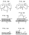
- Figs. 1(a) to 1(f) are schematic views explaining the process of the present invention.
- the present invention resides in a process for repairing circuit connections, which enables reconnection with significantly improved reliability by allowing a peeling liquid to act only on the areas requiring the removal of adhesive and thereby preventing the other areas from being impregnated with the peeling liquid.
- the porous sheet used in the present invention is a sheet having fine pores.
- the porous sheet has no particular restriction as long as it allows the infiltration of a peeling liquid into its whole portion by a capillary action in a short period of time.
- the surface of the porous sheet is contacted with the adhesive remaining on the circuits of circuit connections to be repaired, whereby the peeling liquid contained in the pores of the porous sheet is infiltrated into the adhesive; therefore, the large diameters of the pores make it difficult to accurately set the contact area between the porous sheet and the adhesive.
- the diameters of the pores are preferably 100 ⁇ m or less. If necessary, the surface area of the porous sheet opposite to a surface to be contacted with the remaining adhesive can be sealed in order to ensure no leakage of the peeling liquid from the sealed area, whereby the area of the adhesive to be removed can be limited accurately.
- the sealing of the porous sheet surface can be effected, for example, by heat-melting the porous sheet surface or adhering to the porous sheet surface a coating or a resin film both not attacked by the peeling solution, to seal the surface area of the porous sheet not to be contacted with the adhesive.
- porous sheet examples include fibrous materials such as paper, glass and the like; a non-woven fabric; a porous polytetrafluoroethylene; porous sheets obtained by sintering a thermoplastic resin (e.g. polyethylene); an urethane foam having fine open celled pores, etc.
- a thermoplastic resin e.g. polyethylene
- an urethane foam having fine open celled pores etc.
- the porous sheet obtained from a thermoplastic resin is preferable due to easy surface coating mentioned above by melting with heating or melt adhesion of film with heating.
- the peeling liquid used in the present invention can be any one as long as it can decompose or dissolve the adhesive.
- the peeling liquid there can be mentioned, for example, organic solvents such as toluene, alcohols, ketones and the like; organic acids such as formic acid, acetic acid and the like; inorganic acids such as hydrochloric acid, sulfuric acid and the like; and alkali compounds such as sodium hydroxide, potassium hydroxide and the like. They can be used singly or in combination, or in a solution in an appropriate solvent.
- a peeling liquid of low viscosity and good wettability against porous sheet is preferable because such a peeling liquid has good infiltrability into porous sheet.
- the adhesive used in the present invention has no particular restriction as long as it can be decomposed or dissolved by the peeling liquid.
- the present invention is applicable to, for example, thermoplastic resins such as vinyl acetate resin, polypropylene and the like; highly heat-resistant resins such as polyethersulfone, polyimide, polysulfone and the like, and thermosetting resins such as epoxy resin and the like.
- the present invention is particularly effective to an adhesive having a cross-linked structure, because other methods are difficult to apply to such an adhesive while in the present invention the time of contact of peeling liquid with adhesive can be made long.
- the adhesive which has been decomposed or dissolved by the peeling liquid is infiltrated into the porous sheet and removed.
- the complete removal can be effected by wiping off the residual adhesive with a dry cloth, a dry paper, a dry swab or the like, or with an appropriate material impregnated with a solution incapable of decomposing or dissolving the adhesive.
- an adhesive which can be decomposed or dissolved by the peeling liquid, because such an adhesive can be removed together with the adhesive remaining on circuit surface by the peeling liquid infiltrated into the porous sheet.
- the adhesive there can be used, for example, a rubber-based adhesive, an acrylic resin-based adhesive, or a water-based adhesive.
- the circuit surface contacted with the peeling liquid is cleaned by a conventional process.
- the repair is completed by connecting, to the thus cleaned circuit surface, a cleaned circuit surface of the other circuit substrate or a circuit of a new-substrate, with an adhesive.
- the adhesive contains hard electric conductive particles
- the electric conductive particles can pierce the residual adhesive layer and thereby can establish electrical conduction; accordingly, the circuit substrates separated by mechanical tear-up in the first step can be used in reconnection as they are. This is effective for reduction in repairing cost.
- the peeling liquid contained in the pores of the porous sheet infiltrates into the portion of the adhesive with which the porous sheet surface is contacted, and dissolves or decomposes the adhesive portion, so that only the desired adhesive portion can be removed accurately and the above-mentioned problems are solved.
- the porous sheet has excellent workability because it is a sheet, enables adhesive removal operation in a short period of time, and makes easy the automation of removal operation.
- a sintered sheet made from polyethylene particles of 50 ⁇ m in particle diameter was melt-laminated a polyethylene film.
- the other side of the sintered sheet was coated with an acrylic resin type adhesive to obtain a porous sheet.
- the porous sheet was cut by a hot knife of 200°C to prepare a porous sheet of 10 mm in width and 20 mm in length.
- Fig. 1(b) is a cross-sectional view of the thus obtained connection wherein the ITO circuits 11 on the glass substrate 1 are connected to the circuits 22 on the FPC substrate 2 with the adhesive 3 of anisotropic electric conductivity so as to establish electrical conduction.
- FIG. 1(c) shows the state, wherein the cured adhesive 3 was solidly adhered onto the ITO circuits.
- the glass substrate having no center FPC substrate was used for a test according to the process of the present invention.
- the porous sheet 4 prepared as above and having a coated adhesive layer at the bottom was temporarily adhered onto the adhesive to be removed.
- a glass plate 6 was placed on the porous sheet 4, and a weight 7 was placed thereon for fixing.
- the peeling liquid was infiltrated from the porous sheet into the adhesive for about 10 seconds; then, the porous sheet was removed; the decomposed adhesive was appropriately wiped off with a Teflon®-made spatula; the residual adhesive was wiped off with a swab impregnated with methanol, whereby as shown in Fig. 1(f), the adhesive portion to be removed was completely removed and the ITO circuits 11 therebeneath were completely exposed. Since the pores at the sides 8 of the porous sheet 4 were sealed by the hot knife, there was no leakage of the peeling liquid from the porous sheet and accordingly there was seen no infiltration of the peeling liquid into the adjacent circuits.
- Example 2 The same procedure as in Example 1 was repeated except that the peeling liquid used in Example 1 was changed to a mixture consisting of 74 parts of methylene chloride, 20 parts of formic acid, 5 parts of chloroacetic acid and 1 part of glycerine. There was no increase in connection resistance, either.
- Example 2 The same procedure as in Example 1 was repeated except that there was used, as the porous sheet of 0.5 mm in thickness, a laminate obtained by melt-adhering a polyethylene film to one side of a cellulose-made filter paper specified by JIS P 3801, or 5 ⁇ m in retained particle diameter and coating the other side of the filter paper with an acrylic resin-based adhesive. There was no increase in connection resistance, either.
- the adhesive removal in the above Examples was effected by sliding a swab impregnated with Sun Econ G-430, over the adhesive to decompose the adhesive, then appropriately wiping off the decomposed adhesive with a Teflon-made spatula, and wiping off the residual adhesive with a swab impregnated with methanol.
- connection resistances of FPC circuits adjacent to reconnected FPC circuits increased from the terminals adjacent to reconnected FPC circuits and, out of the total circuits of two FPC substrates adjacent to reconnected FPC circuits, 25 circuits showed a resistance increase of 100 ⁇ or more.
- the present invention can conduct removal of adhesive of strictly specified area and accordingly enables repair of circuit connections with high accuracy and high reliability.
Landscapes
- Engineering & Computer Science (AREA)
- Manufacturing & Machinery (AREA)
- Microelectronics & Electronic Packaging (AREA)
- Combinations Of Printed Boards (AREA)
- Adhesives Or Adhesive Processes (AREA)
- Manufacturing Of Electrical Connectors (AREA)
- Electric Connection Of Electric Components To Printed Circuits (AREA)
Claims (4)
- Verfahren zum Reparieren elektrischer Leiterbahnverbindungen zwischen Leiterbahnsubstraten (1, 2), die einander zugewandt sind und Leiterbahnen (11, 22) aufweisen, die über einen anisotropen Kleber (3) verbunden sind, wobei das Verfahren die folgenden Schritte aufweist:
Abschälen eines zu ersetzenden Leiterbahnsubstrats (2) zusammen mit der Leiterbahn hieran vom anderen Substrat (1), Auflegen eines porösen Bogens (4) vorbestimmter Form auf die Oberfläche des Klebers, der auf dem genannten anderen Substrat verbleibt, Imprägnieren des porösen Bogens (4) mit einer Abschälflüssigkeit, so daß man zeitweise den verbleibenden Kleber mit der Abschälflüssigkeit berührt, dann Entfernen des porösen Bogens (4), der die Abschälflüssigkeit enthält, und Reinigen des verbleibenden Klebers von der Oberfläche des genannten anderen Substrats, um eine gereinigte Leiterbahn auf dem genannten anderen Substrat zu hinterlassen, und nachfolgend Verbinden der gereinigten Leiterbahn mit einer Leiterbahn eines neuen Substrats mit einem anisotropen Kleber. - Verfahren nach Anspruch 1, worin die Oberfläche des porösen Bogens (4), die der Oberfläche zum Berühren des verbleibenden Klebers entgegengesetzt ist, eine abgedichtete Oberfläche ist.
- Verfahren nach Anspruch 1 oder Anspruch 2, worin die Kanten (8) des porösen Bogens (4) abgedichtete Kanten sind.
- Verfahren nach irgendeinem der Ansprüche 1 bis 3, worin die eine oder beide Oberflächen des porösen Bogens (4) teilweise oder vollständig mit einem Kleber beschichtet ist.
Applications Claiming Priority (2)
| Application Number | Priority Date | Filing Date | Title |
|---|---|---|---|
| JP2081984A JPH03283284A (ja) | 1990-03-29 | 1990-03-29 | 回路接続部の補修方法 |
| JP81984/90 | 1990-03-29 |
Publications (3)
| Publication Number | Publication Date |
|---|---|
| EP0449564A2 EP0449564A2 (de) | 1991-10-02 |
| EP0449564A3 EP0449564A3 (en) | 1992-09-23 |
| EP0449564B1 true EP0449564B1 (de) | 1996-09-04 |
Family
ID=13761746
Family Applications (1)
| Application Number | Title | Priority Date | Filing Date |
|---|---|---|---|
| EP91302601A Expired - Lifetime EP0449564B1 (de) | 1990-03-29 | 1991-03-26 | Verfahren für die Reparatur von Leiterbahn-Verbindungen |
Country Status (5)
| Country | Link |
|---|---|
| US (1) | US5155906A (de) |
| EP (1) | EP0449564B1 (de) |
| JP (1) | JPH03283284A (de) |
| KR (1) | KR0183026B1 (de) |
| DE (1) | DE69121750T2 (de) |
Families Citing this family (3)
| Publication number | Priority date | Publication date | Assignee | Title |
|---|---|---|---|---|
| JP2571739B2 (ja) * | 1992-03-10 | 1997-01-16 | 日本アビオニクス株式会社 | 異方性導電フィルムの接着剤除去装置 |
| CN115863499B (zh) * | 2023-02-28 | 2023-04-28 | 成都鸿睿光电科技有限公司 | 基于3d扫描的焊盘修复控制方法、系统、终端及介质 |
| DE102024205292A1 (de) | 2024-06-07 | 2025-12-11 | Robert Bosch Gesellschaft mit beschränkter Haftung | Verfahren zur Ausbildung einer elektrisch leitenden Verbindung |
Family Cites Families (3)
| Publication number | Priority date | Publication date | Assignee | Title |
|---|---|---|---|---|
| US4438561A (en) * | 1981-10-01 | 1984-03-27 | Rogers Corporation | Method of reworking printed circuit boards |
| US4704304A (en) * | 1986-10-27 | 1987-11-03 | International Business Machines Corporation | Method for repair of opens in thin film lines on a substrate |
| EP0360971A3 (de) * | 1988-08-31 | 1991-07-17 | Mitsui Mining & Smelting Co., Ltd. | Substrat für die Montage und sein Herstellungsverfahren und gedruckte Leiterplatte mit Verbinderfunktion und Verbindungsverfahren hierfür |
-
1990
- 1990-03-29 JP JP2081984A patent/JPH03283284A/ja active Pending
-
1991
- 1991-03-19 US US07/672,110 patent/US5155906A/en not_active Expired - Fee Related
- 1991-03-26 DE DE69121750T patent/DE69121750T2/de not_active Expired - Fee Related
- 1991-03-26 EP EP91302601A patent/EP0449564B1/de not_active Expired - Lifetime
- 1991-03-29 KR KR1019910005043A patent/KR0183026B1/ko not_active Expired - Fee Related
Also Published As
| Publication number | Publication date |
|---|---|
| US5155906A (en) | 1992-10-20 |
| DE69121750D1 (de) | 1996-10-10 |
| KR0183026B1 (ko) | 1999-05-15 |
| EP0449564A3 (en) | 1992-09-23 |
| DE69121750T2 (de) | 1997-01-02 |
| EP0449564A2 (de) | 1991-10-02 |
| JPH03283284A (ja) | 1991-12-13 |
Similar Documents
| Publication | Publication Date | Title |
|---|---|---|
| KR950010179B1 (ko) | 접착성 열융착형 인터커넥터 및 그 제조방법 | |
| KR100538956B1 (ko) | 접속재료 | |
| US5122215A (en) | Method of producing electrically conductive anisotropic heat sealing connector members | |
| EP0449564B1 (de) | Verfahren für die Reparatur von Leiterbahn-Verbindungen | |
| US4226659A (en) | Method for bonding flexible printed circuitry to rigid support plane | |
| JP3472987B2 (ja) | 接続部材の製造法及びその製造装置 | |
| JPH02877B2 (de) | ||
| JPH0615429Y2 (ja) | 接着性熱融着形コネクタ | |
| KR920005071B1 (ko) | 배선기판 | |
| JPH06223945A (ja) | 回路接続部の補修方法 | |
| JP2003208931A (ja) | 接続部材 | |
| JPH0696620A (ja) | 異方性導電材料および該材料を用いた回路の接続方法並びに電気回路基板 | |
| JP2828851B2 (ja) | 電子部品の修復方法 | |
| JP3129218B2 (ja) | ファインピッチコネクタ部材 | |
| JPS5953717B2 (ja) | プリント回路基板上にヒ−トシ−ルコネクタとの接触端子部を製造する方法 | |
| JP2545097Y2 (ja) | セパレ−タ−付きヒ−トシ−ルコネクタ− | |
| JP2002246701A (ja) | フレキシブルプリント基板及びヒートシールコネクタ | |
| JP2594644B2 (ja) | ピン付きヒートシールコネクタの製造方法 | |
| KR20040061046A (ko) | 인쇄 회로 기판 적층 방법 | |
| JPH04169080A (ja) | 加熱硬化型異方導電接続部材 | |
| JPS6215777A (ja) | フイルム状コネクタ及びその製造方法 | |
| JP2595140Y2 (ja) | 電子部品接合用接着フィルム | |
| JPH07321158A (ja) | フィルムキャリアおよびそれを用いた液晶表示素子とその製法 | |
| JP3129217B2 (ja) | ファインピッチコネクタ部材 | |
| JP2000197856A (ja) | 異方性導電接着剤の残渣除去方法 |
Legal Events
| Date | Code | Title | Description |
|---|---|---|---|
| PUAI | Public reference made under article 153(3) epc to a published international application that has entered the european phase |
Free format text: ORIGINAL CODE: 0009012 |
|
| AK | Designated contracting states |
Kind code of ref document: A2 Designated state(s): DE FR GB IT NL |
|
| PUAL | Search report despatched |
Free format text: ORIGINAL CODE: 0009013 |
|
| AK | Designated contracting states |
Kind code of ref document: A3 Designated state(s): DE FR GB IT NL |
|
| 17P | Request for examination filed |
Effective date: 19930127 |
|
| 17Q | First examination report despatched |
Effective date: 19931110 |
|
| GRAH | Despatch of communication of intention to grant a patent |
Free format text: ORIGINAL CODE: EPIDOS IGRA |
|
| GRAH | Despatch of communication of intention to grant a patent |
Free format text: ORIGINAL CODE: EPIDOS IGRA |
|
| GRAA | (expected) grant |
Free format text: ORIGINAL CODE: 0009210 |
|
| AK | Designated contracting states |
Kind code of ref document: B1 Designated state(s): DE FR GB IT NL |
|
| ITF | It: translation for a ep patent filed | ||
| ET | Fr: translation filed | ||
| REF | Corresponds to: |
Ref document number: 69121750 Country of ref document: DE Date of ref document: 19961010 |
|
| PLBE | No opposition filed within time limit |
Free format text: ORIGINAL CODE: 0009261 |
|
| STAA | Information on the status of an ep patent application or granted ep patent |
Free format text: STATUS: NO OPPOSITION FILED WITHIN TIME LIMIT |
|
| 26N | No opposition filed | ||
| PGFP | Annual fee paid to national office [announced via postgrant information from national office to epo] |
Ref country code: FR Payment date: 20010313 Year of fee payment: 11 |
|
| PGFP | Annual fee paid to national office [announced via postgrant information from national office to epo] |
Ref country code: DE Payment date: 20010319 Year of fee payment: 11 |
|
| PGFP | Annual fee paid to national office [announced via postgrant information from national office to epo] |
Ref country code: GB Payment date: 20010321 Year of fee payment: 11 |
|
| PGFP | Annual fee paid to national office [announced via postgrant information from national office to epo] |
Ref country code: NL Payment date: 20010330 Year of fee payment: 11 |
|
| REG | Reference to a national code |
Ref country code: GB Ref legal event code: IF02 |
|
| PG25 | Lapsed in a contracting state [announced via postgrant information from national office to epo] |
Ref country code: GB Free format text: LAPSE BECAUSE OF NON-PAYMENT OF DUE FEES Effective date: 20020326 |
|
| PG25 | Lapsed in a contracting state [announced via postgrant information from national office to epo] |
Ref country code: NL Free format text: LAPSE BECAUSE OF NON-PAYMENT OF DUE FEES Effective date: 20021001 Ref country code: DE Free format text: LAPSE BECAUSE OF NON-PAYMENT OF DUE FEES Effective date: 20021001 |
|
| GBPC | Gb: european patent ceased through non-payment of renewal fee |
Effective date: 20020326 |
|
| PG25 | Lapsed in a contracting state [announced via postgrant information from national office to epo] |
Ref country code: FR Free format text: LAPSE BECAUSE OF NON-PAYMENT OF DUE FEES Effective date: 20021129 |
|
| NLV4 | Nl: lapsed or anulled due to non-payment of the annual fee |
Effective date: 20021001 |
|
| REG | Reference to a national code |
Ref country code: FR Ref legal event code: ST |
|
| PG25 | Lapsed in a contracting state [announced via postgrant information from national office to epo] |
Ref country code: IT Free format text: LAPSE BECAUSE OF NON-PAYMENT OF DUE FEES;WARNING: LAPSES OF ITALIAN PATENTS WITH EFFECTIVE DATE BEFORE 2007 MAY HAVE OCCURRED AT ANY TIME BEFORE 2007. THE CORRECT EFFECTIVE DATE MAY BE DIFFERENT FROM THE ONE RECORDED. Effective date: 20050326 |