EP0449474A2 - Liaison de données optique couplée en courant continu utilisant la transmission différentielle - Google Patents
Liaison de données optique couplée en courant continu utilisant la transmission différentielle Download PDFInfo
- Publication number
- EP0449474A2 EP0449474A2 EP91302306A EP91302306A EP0449474A2 EP 0449474 A2 EP0449474 A2 EP 0449474A2 EP 91302306 A EP91302306 A EP 91302306A EP 91302306 A EP91302306 A EP 91302306A EP 0449474 A2 EP0449474 A2 EP 0449474A2
- Authority
- EP
- European Patent Office
- Prior art keywords
- array
- devices
- logic
- output
- semiconductor optical
- Prior art date
- Legal status (The legal status is an assumption and is not a legal conclusion. Google has not performed a legal analysis and makes no representation as to the accuracy of the status listed.)
- Withdrawn
Links
Images

Classifications
-
- H—ELECTRICITY
- H04—ELECTRIC COMMUNICATION TECHNIQUE
- H04B—TRANSMISSION
- H04B10/00—Transmission systems employing electromagnetic waves other than radio-waves, e.g. infrared, visible or ultraviolet light, or employing corpuscular radiation, e.g. quantum communication
- H04B10/03—Arrangements for fault recovery
- H04B10/032—Arrangements for fault recovery using working and protection systems
Definitions
- the present invention relates to a DC-coupled optical data link utilizing differential transmission and, more particularly, to a system which utilizes an array of paired transmitting devices and an array of paired receiving devices to achieve communication, with one device of each pair dedicated to transmission of a logic "0" and the other dedicated to transmission of a logic "1".
- the present invention which relates to a DC-coupled optical data link utilizing differential transmission and, more particularly, to a system which utilizes an array of paired transmitting devices and an array of paired receiving devices, coupled together by an array of paired optical signal paths, to provide transmission suitable for optical backplane applications.
- a pair of transmitting devices are used to transmit a given data stream, with the first device being activated to transmit a logic "1" and the second device being activated to transmit a logic "0".
- a pair of receiving devices are used to recover the data stream, where the data is recovered by comparing the photocurrent outputs from the pair of devices.
- an array of 2N transmitting devices, coupled in pairs to a set of data inputs may be used to form a set of N data channels for simultaneously transmitting N separate data streams. It is to be understood that individual data signals may be multiplexed together to form a single data stream so that the array system of the present invention is actually capable of transmitting MxN signals, where M is number of data signals/stream.
- bidirectional communication is achieved by utilizing the semiconductor devices at each end of the data channel as both transmit and receive devices. Accordingly, transmit and receive circuitry is then located at each end of the channel.
- amplification of the transmitted signal may be obtained, in another embodiment of the present invention, by using a laser gain medium, for example, a laser amplifier, coupled to each pair of waveguides. Since the gain medium will preferentially amplify the transmitted data signal with respect to any background noise present along the inactive waveguide, the amplifier also serves as a filter to the communication system.
- a laser gain medium for example, a laser amplifier
- An advantage of the present invention is that by utilizing pairs of transmitters, optical paths and receivers to transmit data, the relative DC level of the pair of signals is unchanging (i.e., fixed at zero), allowing relatively simple emitter-coupled logic (ECL) transmitter and receiver circuits to be used.
- ECL emitter-coupled logic
- An additional advantage may be realized in one embodiment of the present invention where integrated arrays of transmitter and receiver optical devices are used. Integration provides for inherent matching of components, resulting in substantially equal power being emitted from the transmitting devices, and substantially equal photocurrents being developed by the receiving devices.
- the use of integrated arrays will provide further advantages to the system in terms of inter-device tracking as a function of, for example, temperature, age or alignment. The match inherent in optical devices allows for further simplification in the electronic circuitry.
- the need to provide special signal encoding for the purposes of clock recovery may be eliminated by reserving one pair of lines for transmission of a system clock. Therefore, for a conventional fiber ribbon cable of twelve (or eighteen) individual fibers, one clock signal and five (or eight) data streams (each stream having one or more separate data signals) may be simultaneously transmitted.
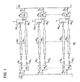
- FIG. 1 An exemplary differential array optical data link 10 of the present invention is illustrated in FIG. 1.
- a data link may advantageously be utilized as an optical backplane interconnect between a first equipment component 12 (for example, a personal computer) and a second equipment component 14 (for example, a mass storage device or cache memory device).
- each data channel is associated with two distinguishable (e.g., separate polarizations or separate fibers) optical signal paths, one path for transmitting a logic "0" and the other for transmitting a logic "1".
- the optical signal path will be discussed in terms of an optical fiber.
- the present invention is not limited to utilizing optical fibers as the optical transmission media.
- a first data stream D1 is applied as an input to a first transmitter 161, the output of transmitter 161 being coupled to a pair of light emitting devices 181, 201, where devices 181, 201 may be lasers or LEDs.
- An exemplary transmitter 16 i will be discussed in detail below in association with FIG. 6.
- transmitter 161 is configured to activate device 181 to transmit a logic "0" and activate device 201 to transmit a logic "1".
- device 181 is coupled to the near end of optical fiber 221 and device 201 is coupled to the near end of fiber 241.
- the far ends of fibers 221 and 241 are coupled to a pair of optical devices 261 and 281, respectively, where devices 261,281 may comprise PIN or avalanche photodiodes, or any other suitable optical receiving devices.
- the electrical output signals from devices 261, 281 are applied as inputs to a receiver 301 which recovers the transmitted data stream D1.
- Receiving devices 261,281 may be considered as forming part of a receiver circuit 301, where an exemplary receiver 30 i will be discussed in detail below in association with FIG. 7.
- the system of the present invention is particularly advantageous for array applications with multiple LED (or laser) and PIN arrays (or alternatively, arrays of other transmitting and.or receiving devices).
- additional data streams D2, ..., D N are illustrated as applied to the inputs of transmitters 162,..., 16 N .
- Devices 182, 202 through 18 N , 20 N are then activated in accordance with the data streams and the light outputs are propagated along fibers 222, 242 through 22 N , 24 N to receivers 302 - 30 N .
- Twu et al. appearing in Electronic Letters , Vol. 24, No. 2, June 1988 at pp. 743-4 discusses a particular fabrication technique suitable for laser array applications. Fabrication techniques for LED and PIN arrays are described in an article entitled "12-channel Ph and LED arrays and their packaging for 1.3 ⁇ m applications", by Y. Ota et al., appearing in Proceedings SPIE , Vol. 839, 1988 at pp. 143-7. Since a monolithic array of optical devices will have been subject to identical processing sequences, the devices will contain essentially identical performance characteristics (in terms of temperature tracking, aging, alignment, etc.).
- the preferred embodiment with present technology would consist of a conventional twelve (or eighteen) fiber ribbon cable. Therefore, the embodiment would include a set of six (or nine) physical data channels.
- the number of data signals transmitted over each channel may be increased. In this case, the transmission of a frame clock becomes a requirement and one of the six (nine) channels may be reserved for this purpose.
- the five (eight) remaining data channels may be multiplexed to carry M separate separate data signals (where M may vary from channel to channel).
- a differential data link of the present invention may also be configured as a bidirectional communication system.
- An exemplary bidirectional differential data link 100 is illustrated in FIG. 2. Similar to the arrangement of FIG. 1, link 100 is utilized to provide communication between first equipment component 12 and second equipment component 14 over a plurality of N data channels, each channel comprising a pair of optical fibers 22 i , 24 i . For the sake of clarity, only the "ith" channel is illustrated in FIG. 2. It is to be understood that in implementation, bidirectional data link 10, like data link 10 of FIG. 1, comprises a plurality of N data channels, each constructed in a manner similar to that shown in FIG. 2. In accordance with the present invention, bidirectional communication is achieved by including optical transmitting and receiving devices with both components 12 and 14.
- a second pair of transmitting devices 18′ i , 20′ i are co-located with receiving devices 26 i , 28 i at component 14.
- a second pair of receiving devices 26′ i , 28′ i are co-located with transmitting devices 18 i , 20 i at component 12.
- bidirectional data link 100 In operation of bidirectional data link 100, communication from equipment component 12 to equipment component 14 occurs as discussed above with the embodiment of FIG. 1.
- a data signal D′ i from equipment component 14 is applied as an input to differential transmitter circuit 16′ i .
- the pair of outputs from circuit 16′ i are then applied as inputs to transmitting devices 18′ i , 20′ i for propagation over the "ith" communication channel (via fibers 22 i , 24 i ) to equipment component 12.
- the received signal is coupled to the pair of receiving devices 26′ i , 30′ i for conversion into an electrical signal.
- fiber 22 i is modified to include a first splitter 102 at component 12 and a second splitter 104 at component 14.
- fiber 24 i is modified to include a first splitter 106 at component 12 and a second splitter 108 at component 14.
- splitter 102 couples transmitting device 18 i and receiving device 26′ i to fiber 22 i
- splitter 104 couples receiving device 26 i and transmitting device 18′ i to fiber 22 i .
- Splitters 106,108 provide a similar function with respect to devices 20 i , 28′ i , 28 i , 20′ i and fiber 24 i .
- the arrangement of FIG. 2 is capable of providing full duplex, bidirectional communication between equipment components 12 and 14.
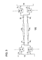
- a half duplex arrangement 120 as illustrated in FIG. 3, may be the preferred alternative.
- the same pair of devices for example, devices 18 i , 20 i at the near end and 26 i , 28 i at the far end, are used as both transmitting and receiving devices.
- an LED may behave as either a light emitter or light receptor, depending upon the bias applied thereto.
- arrays of LEDs may be used in this particular embodiment to provide bidirectional communication.
- a transmitter circuit 16′ i is co-located with receiver circuit 30 i at component 14 to provide the return data signal D′ i to devices 26 i , 28 i .
- a receiver circuit 30′ i is co-located with transmitter circuit 16 i at component 12 to receive electrical output from devices 18 i , 20 i and enable recovery of the transmitted return signal D′ i .
- the co-located transmitter and receiver circuitry may be integrated on a single substrate to decrease the overall size of the data link.
- a system clock would allow, for example, component 12 to transmit during only a first designated time period ⁇ 1, and component 14 to transmit during only a second designated time period ⁇ 2. It is to be understood that there exist many other means of controlling the communication of information between the two equipment components 12 and 14.
- An advantage of the present invention is the use of differential transmission in the form of a pair of paths used to form a single data channel. Differential transmission allows for the receiver circuitry to be formed with differential logic, with the threshold level set at zero.
- a receiver 30 i (30′ i ) merely compares the photocurrent outputs from devices 26 i ,28 i (18 i , 20 i ) and forms the recovered data signal by determining which device produces the largest signal. In particular, if the output from device 26 i (18 i ) is greater, the recovered bit is defined as a logic "0". Alternatively, of the output from device 28 i (20 i ) is greater, the recovered bit is defined as a logic "1".
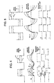
- FIG. 4 is illustrative of the pulse width distortion problem.
- a fixed threshold DC level TH is used to determine which logic bit has been received.
- FIG. 4 illustrates three different signal power levels, indicated by the appropriate letters L (low), S (standard) and H (high).
- L (low) low
- S standard
- H high
- the resultant output pulse from the receiver is also illustrated.
- the transitions are seen to occur at points C and D, and the output pulse is of the shape illustrated below the received signals.
- the receiver is overdriven and the signal power exceeds the specified value, the transitions are shown to occur at points E and F, with the resulting output data signal as shown.
- pulse width distortion will be present in this system, as indicated by ⁇ and ⁇ in FIG. 4.
- an "automatic threshold" setting may be utilized which continuously adjusts to the received signal power level.
- this particular type of receiver is known to fail in the absence of both "1"'s and "0"'s (or during long runs of either "1"'s or "0"'s).
- the threshold TH of the receiver is set to provide equal channel current levels so that a differential DC level of zero is achieved.
- the transitions between logic "1" to logic “0" are therefore determined only by the zero crossings of the received signal.
- L, S and H it is shown in FIG. 5 that the zero-crossing is independent of the received signal power. Therefore, the recovered data signal from the differential receiver will be essentially independent of the strength of the received signal.
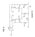
- FIG. 6 An exemplary transmitter circuit is illustrated in FIG. 6.
- the differential design exploits the inherent matching of devices 16 and 18, as discussed above, to provide equal emitted power, minimum noise injection.
- data signal D i is applied as the input to amplifier 40, where amplifier 40 is configured to provide a pair of output signals of opposite value (referred to as non-inverting and inverting outputs).
- the non-inverting output is applied to the base of a first transistor 42, the collector of transistor 42 being grounded.
- the inverting output from amplifier 40 is applied as the input to the base of a second transistor 44, where the collector of transistor 44 is also grounded.
- the bases of transistors 42,44 are coupled through resistors 46,48 to a power supply rail 50.
- Emitters of transistors 42,44 are coupled to LEDs 16 and 18, respectively, where LEDS 16,18 are also coupled through resistors 52 to power supply rail 50.
- D i data signal
- transistor 42 will be turned on and activate LED 16.
- the inverting output from amplifier 40 will go high and turn on transistor 44.
- the activation of transistor 44 will cause LED 18 to emit light.
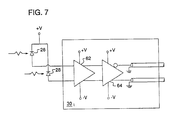
- Receiver 30 i contains a differential amplifier 62, where photodiode 26 is coupled to an inverting input of amplifier 62 and photodiode 28 is coupled to the noninverting input of amplifier 62.
- the complementary outputs from amplifier 62 are coupled to the inputs of a comparator 66. Since differential signaling is used, the DC level of the input to comparator 66 is maintained at a relative DC zero level, allowing the amplifiers to be directly connected to comparator 66 without any capacitive interconnection.
- Comparator 66 maintains a constant threshold TH, as discussed in association with FIG. 5, and provides the recovered data signal as a function of the input of the greatest magnitude.
- the transmitter circuit of FIG. 6 may be replicated for each data channel and integrated as a single monolithic unit.
- the receiver circuit of FIG. 7 may be replicated and integrated.
- the resultant array communication when used with an optical fiber ribbon cable, enjoys the maximum benefits of matching the optical and electrical characteristics of each data channel.
Landscapes
- Physics & Mathematics (AREA)
- Electromagnetism (AREA)
- Engineering & Computer Science (AREA)
- Computer Networks & Wireless Communication (AREA)
- Signal Processing (AREA)
- Optical Communication System (AREA)
Applications Claiming Priority (2)
| Application Number | Priority Date | Filing Date | Title |
|---|---|---|---|
| US07/499,225 US5138475A (en) | 1990-03-26 | 1990-03-26 | Dc-coupled optical data link utilizing differential transmission |
| US499225 | 1990-03-26 |
Publications (2)
| Publication Number | Publication Date |
|---|---|
| EP0449474A2 true EP0449474A2 (fr) | 1991-10-02 |
| EP0449474A3 EP0449474A3 (en) | 1992-09-09 |
Family
ID=23984361
Family Applications (1)
| Application Number | Title | Priority Date | Filing Date |
|---|---|---|---|
| EP19910302306 Withdrawn EP0449474A3 (en) | 1990-03-26 | 1991-03-18 | Dc-coupled optical data link utilizing differential transmission |
Country Status (3)
| Country | Link |
|---|---|
| US (1) | US5138475A (fr) |
| EP (1) | EP0449474A3 (fr) |
| JP (1) | JPH04223628A (fr) |
Cited By (2)
| Publication number | Priority date | Publication date | Assignee | Title |
|---|---|---|---|---|
| FR2737628A1 (fr) * | 1995-08-01 | 1997-02-07 | Motorola Inc | Appareil et procede de transport de signaux de positionnement temporel de trames, de signaux de positionnement temporel de donnees et de signaux de donnees |
| EP1261159A1 (fr) * | 2001-05-25 | 2002-11-27 | Lucent Technologies Inc. | Sytème optique différentiel a multiplexage par reparition en longueur d'onde dense |
Families Citing this family (11)
| Publication number | Priority date | Publication date | Assignee | Title |
|---|---|---|---|---|
| US5323409A (en) * | 1991-12-05 | 1994-06-21 | Honeywell Inc. | Wavelength stabilization |
| JP2746197B2 (ja) * | 1995-04-21 | 1998-04-28 | 日本電気株式会社 | 光送信装置 |
| US5541759A (en) * | 1995-05-09 | 1996-07-30 | Microsym Computers, Inc. | Single fiber transceiver and network |
| KR0159663B1 (ko) * | 1995-10-28 | 1998-12-01 | 김광호 | 광데이타 전송 이중화를 구현한 광데이타 전송장치 |
| US6310707B1 (en) * | 1996-10-25 | 2001-10-30 | Seiko Epson Corporation | Optical wireless data communication system, and transmitter and receiver used therefor |
| GB2346300B (en) * | 1999-01-28 | 2003-12-03 | Roke Manor Research | Data filtering apparatus and method of filtering a plurality of data signals |
| US20030235415A1 (en) * | 2002-06-21 | 2003-12-25 | Peters Frank H. | Optical communication devices and optical communication methods |
| US20050089331A1 (en) * | 2003-10-03 | 2005-04-28 | Near Margalit | Assured connectivity fiber-optic communications link |
| US20050089332A1 (en) * | 2003-10-03 | 2005-04-28 | Near Margalit | Long reach optical transmission over a single fiber |
| JP2010028751A (ja) * | 2008-07-24 | 2010-02-04 | Toshiba Corp | コンプリメンタリー光配線装置 |
| JP2010136244A (ja) * | 2008-12-08 | 2010-06-17 | Toshiba Corp | 送信回路およびコンプリメンタリー光配線システム |
Citations (7)
| Publication number | Priority date | Publication date | Assignee | Title |
|---|---|---|---|---|
| JPS5314503A (en) * | 1976-07-26 | 1978-02-09 | Fujitsu Ltd | Photo-communication system |
| JPS57106247A (en) * | 1980-12-24 | 1982-07-02 | Hitachi Ltd | Analogue optical communication device |
| WO1982002632A1 (fr) * | 1981-01-16 | 1982-08-05 | Western Electric Co | Dispositif de communication optique pour la reduction de la distorsion harmonique |
| FR2500972A1 (fr) * | 1981-02-27 | 1982-09-03 | France Etat | Procede et dispositif de transmission de signaux analogiques rapides sur fibres optiques |
| FR2563672A1 (fr) * | 1984-04-26 | 1985-10-31 | Lignes Telegraph Telephon | Systeme de transmission d'informations numeriques sur fibre optique |
| JPS6189735A (ja) * | 1984-10-08 | 1986-05-07 | Nippon Telegr & Teleph Corp <Ntt> | 光通信方式の時分割方向制御伝送方式 |
| EP0201370A1 (fr) * | 1985-04-02 | 1986-11-12 | Thomson-Csf | Système de transmission d'information de type analogique par conducteur optique, à très faible consommation |
Family Cites Families (17)
| Publication number | Priority date | Publication date | Assignee | Title |
|---|---|---|---|---|
| US4052611A (en) * | 1975-04-22 | 1977-10-04 | The United States Of America As Represented By The Secretary Of The Navy | High speed fiber optic communication link |
| US4330870A (en) * | 1980-09-05 | 1982-05-18 | Datapoint Corporation | Optical data link |
| US4338732A (en) * | 1980-12-15 | 1982-07-13 | Allis-Chalmers Corporation | Lifter cage for asphalt plant, dryers and drum mixers |
| JPS5824258A (ja) * | 1981-08-06 | 1983-02-14 | Sumitomo Electric Ind Ltd | 光通信受信回路 |
| FR2520174A1 (fr) * | 1982-01-15 | 1983-07-22 | Lignes Telegraph Telephon | Systeme de transmission de signaux numeriques sur fibre optique |
| US4497068A (en) * | 1982-01-25 | 1985-01-29 | Eaton Corporation | Encoding system for optic data link |
| JPS58181343A (ja) * | 1982-04-16 | 1983-10-24 | Nippon Denso Co Ltd | 光信号伝送回路 |
| US4495655A (en) * | 1982-07-27 | 1985-01-22 | General Electric Company | Testable optically isolated control circuit |
| US4569059A (en) * | 1984-05-25 | 1986-02-04 | Fish Franklin H | Optically coupled differential data link |
| US4703471A (en) * | 1985-01-02 | 1987-10-27 | General Electric Company | Monolithically integrated electro-optical multiplexer/demultiplexer |
| JPS6212221A (ja) * | 1985-07-10 | 1987-01-21 | Fujitsu Ltd | 光伝送方式 |
| JPS62234432A (ja) * | 1986-04-04 | 1987-10-14 | Hitachi Ltd | 双方向光伝送方法とその装置 |
| GB8616873D0 (en) * | 1986-07-10 | 1986-08-20 | British Telecomm | Optical telecommunications system |
| US4784001A (en) * | 1987-07-13 | 1988-11-15 | Emerson Electric Co. | Magnetic flowmeter with isolation amplifier and ranging circuit therefor and method |
| US4989934A (en) * | 1987-11-13 | 1991-02-05 | Kopin Corporation | Monolithic integrated transceiver of III-V devices on silicon |
| US4870637A (en) * | 1987-12-24 | 1989-09-26 | American Telephone And Telegraph Company | Optical backplane |
| US4979185A (en) * | 1989-10-30 | 1990-12-18 | Texas Instruments Incorporated | High speed serial data link |
-
1990
- 1990-03-26 US US07/499,225 patent/US5138475A/en not_active Expired - Lifetime
-
1991
- 1991-03-18 EP EP19910302306 patent/EP0449474A3/en not_active Withdrawn
- 1991-03-22 JP JP3081234A patent/JPH04223628A/ja active Pending
Patent Citations (7)
| Publication number | Priority date | Publication date | Assignee | Title |
|---|---|---|---|---|
| JPS5314503A (en) * | 1976-07-26 | 1978-02-09 | Fujitsu Ltd | Photo-communication system |
| JPS57106247A (en) * | 1980-12-24 | 1982-07-02 | Hitachi Ltd | Analogue optical communication device |
| WO1982002632A1 (fr) * | 1981-01-16 | 1982-08-05 | Western Electric Co | Dispositif de communication optique pour la reduction de la distorsion harmonique |
| FR2500972A1 (fr) * | 1981-02-27 | 1982-09-03 | France Etat | Procede et dispositif de transmission de signaux analogiques rapides sur fibres optiques |
| FR2563672A1 (fr) * | 1984-04-26 | 1985-10-31 | Lignes Telegraph Telephon | Systeme de transmission d'informations numeriques sur fibre optique |
| JPS6189735A (ja) * | 1984-10-08 | 1986-05-07 | Nippon Telegr & Teleph Corp <Ntt> | 光通信方式の時分割方向制御伝送方式 |
| EP0201370A1 (fr) * | 1985-04-02 | 1986-11-12 | Thomson-Csf | Système de transmission d'information de type analogique par conducteur optique, à très faible consommation |
Non-Patent Citations (3)
| Title |
|---|
| PATENT ABSTRACTS OF JAPAN vol. 10, no. 263 (E-435)(2319) 9 September 1986 & JP-A-61 089 735 ( NTT ) * |
| PATENT ABSTRACTS OF JAPAN vol. 2, no. 51 (E-78)(926) 12 April 1978 & JP-A-53 014 503 ( FUJITSU ) * |
| PATENT ABSTRACTS OF JAPAN vol. 6, no. 194 (E-134)(1072) 2 October 1982 & JP-A-57 106 247 ( HITACHI SEISAKUSHO ) * |
Cited By (5)
| Publication number | Priority date | Publication date | Assignee | Title |
|---|---|---|---|---|
| FR2737628A1 (fr) * | 1995-08-01 | 1997-02-07 | Motorola Inc | Appareil et procede de transport de signaux de positionnement temporel de trames, de signaux de positionnement temporel de donnees et de signaux de donnees |
| GB2303986A (en) * | 1995-08-01 | 1997-03-05 | Motorola Inc | Two fibre method for conveying frame timing, data timing, and data |
| GB2303986B (en) * | 1995-08-01 | 1999-08-11 | Motorola Inc | Apparatus and method for conveying frame timing, data timing, and data |
| EP1261159A1 (fr) * | 2001-05-25 | 2002-11-27 | Lucent Technologies Inc. | Sytème optique différentiel a multiplexage par reparition en longueur d'onde dense |
| US7072592B2 (en) | 2001-05-25 | 2006-07-04 | Lucent Technologies Inc. | Differential dense wavelength division multiplexing (DDWDM) in optical systems |
Also Published As
| Publication number | Publication date |
|---|---|
| US5138475A (en) | 1992-08-11 |
| EP0449474A3 (en) | 1992-09-09 |
| JPH04223628A (ja) | 1992-08-13 |
Similar Documents
| Publication | Publication Date | Title |
|---|---|---|
| US5138475A (en) | Dc-coupled optical data link utilizing differential transmission | |
| US6947672B2 (en) | High-speed optical data links | |
| US9048958B2 (en) | High-speed optical fiber link and a method for communicating optical data signals | |
| US8406634B2 (en) | Method and apparatus for optical signaling | |
| US5923451A (en) | Means for connecting electronic devices for communication with one another | |
| US5105293A (en) | Differential optical signal transmission using a single optical fiber | |
| US20060126993A1 (en) | SOI-based optical interconnect arrangement | |
| US20050036789A1 (en) | Free space optical bus | |
| US4051363A (en) | Split-path receiver for fiber optics application | |
| US7072590B2 (en) | Fiber optic receiver with an adjustable bandwidth post-amplifier | |
| US7536107B2 (en) | Optical offset signal cancellation for optical receiver | |
| Li et al. | Fully differential optical interconnections for high-speed digital systems | |
| CN208572096U (zh) | 双收双发设备及传输系统 | |
| CN100380851C (zh) | 双向光连接中降低串扰的方法和装置 | |
| Chujo et al. | A 25-Gb/s× 4-Ch, 8× 8 mm2, 2.8-mm thick compact optical transceiver module for on-board optical interconnect | |
| US5636047A (en) | Optical interconnection system | |
| Nishikido et al. | Multigigabit multichannel optical interconnection module for broadband switching system | |
| Akahori et al. | Hybrid integrated differential photoreceiver module for photonic packet switching systems using a planar lightwave circuit platform | |
| US7505497B2 (en) | Laser driver for high speed short distance links | |
| US8247756B1 (en) | Bi-directional data and signal channels in optical interconnects | |
| EP1417786A1 (fr) | Liaisons optiques de donnees a grande vitesse | |
| US4864650A (en) | Expansion network for increasing the number of subscriber terminations at a passive optical bus system comprising optical mixers | |
| US6751217B1 (en) | Combined selector switch and serial multi-Gb/s data pulse receiver | |
| GB2237949A (en) | Optical networks | |
| HORIMATSU et al. | Optical parallel interconnection based on group multiplexing and coding technique |
Legal Events
| Date | Code | Title | Description |
|---|---|---|---|
| PUAI | Public reference made under article 153(3) epc to a published international application that has entered the european phase |
Free format text: ORIGINAL CODE: 0009012 |
|
| AK | Designated contracting states |
Kind code of ref document: A2 Designated state(s): DE GB |
|
| PUAL | Search report despatched |
Free format text: ORIGINAL CODE: 0009013 |
|
| AK | Designated contracting states |
Kind code of ref document: A3 Designated state(s): DE GB |
|
| 17P | Request for examination filed |
Effective date: 19930225 |
|
| RAP3 | Party data changed (applicant data changed or rights of an application transferred) |
Owner name: AT&T CORP. |
|
| 17Q | First examination report despatched |
Effective date: 19950731 |
|
| STAA | Information on the status of an ep patent application or granted ep patent |
Free format text: STATUS: THE APPLICATION HAS BEEN WITHDRAWN |
|
| 18W | Application withdrawn |
Withdrawal date: 19951124 |