EP0448713B1 - Halbleiteranordnung - Google Patents
Halbleiteranordnung Download PDFInfo
- Publication number
- EP0448713B1 EP0448713B1 EP89908519A EP89908519A EP0448713B1 EP 0448713 B1 EP0448713 B1 EP 0448713B1 EP 89908519 A EP89908519 A EP 89908519A EP 89908519 A EP89908519 A EP 89908519A EP 0448713 B1 EP0448713 B1 EP 0448713B1
- Authority
- EP
- European Patent Office
- Prior art keywords
- substrate
- semiconductor chip
- coupling hole
- semiconductor
- tapered portion
- Prior art date
- Legal status (The legal status is an assumption and is not a legal conclusion. Google has not performed a legal analysis and makes no representation as to the accuracy of the status listed.)
- Expired - Lifetime
Links
Images
Classifications
-
- H—ELECTRICITY
- H10—SEMICONDUCTOR DEVICES; ELECTRIC SOLID-STATE DEVICES NOT OTHERWISE PROVIDED FOR
- H10W—GENERIC PACKAGES, INTERCONNECTIONS, CONNECTORS OR OTHER CONSTRUCTIONAL DETAILS OF DEVICES COVERED BY CLASS H10
- H10W72/00—Interconnections or connectors in packages
- H10W72/30—Die-attach connectors
-
- H—ELECTRICITY
- H10—SEMICONDUCTOR DEVICES; ELECTRIC SOLID-STATE DEVICES NOT OTHERWISE PROVIDED FOR
- H10D—INORGANIC ELECTRIC SEMICONDUCTOR DEVICES
- H10D62/00—Semiconductor bodies, or regions thereof, of devices having potential barriers
- H10D62/10—Shapes, relative sizes or dispositions of the regions of the semiconductor bodies; Shapes of the semiconductor bodies
- H10D62/117—Shapes of semiconductor bodies
-
- H—ELECTRICITY
- H10—SEMICONDUCTOR DEVICES; ELECTRIC SOLID-STATE DEVICES NOT OTHERWISE PROVIDED FOR
- H10W—GENERIC PACKAGES, INTERCONNECTIONS, CONNECTORS OR OTHER CONSTRUCTIONAL DETAILS OF DEVICES COVERED BY CLASS H10
- H10W70/00—Package substrates; Interposers; Redistribution layers [RDL]
- H10W70/01—Manufacture or treatment
- H10W70/05—Manufacture or treatment of insulating or insulated package substrates, or of interposers, or of redistribution layers
- H10W70/093—Connecting or disconnecting other interconnections thereto or therefrom, e.g. connecting bond wires or bumps
-
- H—ELECTRICITY
- H10—SEMICONDUCTOR DEVICES; ELECTRIC SOLID-STATE DEVICES NOT OTHERWISE PROVIDED FOR
- H10W—GENERIC PACKAGES, INTERCONNECTIONS, CONNECTORS OR OTHER CONSTRUCTIONAL DETAILS OF DEVICES COVERED BY CLASS H10
- H10W70/00—Package substrates; Interposers; Redistribution layers [RDL]
- H10W70/60—Insulating or insulated package substrates; Interposers; Redistribution layers
- H10W70/611—Insulating or insulated package substrates; Interposers; Redistribution layers for connecting multiple chips together
-
- H—ELECTRICITY
- H10—SEMICONDUCTOR DEVICES; ELECTRIC SOLID-STATE DEVICES NOT OTHERWISE PROVIDED FOR
- H10W—GENERIC PACKAGES, INTERCONNECTIONS, CONNECTORS OR OTHER CONSTRUCTIONAL DETAILS OF DEVICES COVERED BY CLASS H10
- H10W70/00—Package substrates; Interposers; Redistribution layers [RDL]
- H10W70/60—Insulating or insulated package substrates; Interposers; Redistribution layers
- H10W70/62—Insulating or insulated package substrates; Interposers; Redistribution layers characterised by their interconnections
- H10W70/63—Vias, e.g. via plugs
- H10W70/635—Through-vias
-
- H—ELECTRICITY
- H10—SEMICONDUCTOR DEVICES; ELECTRIC SOLID-STATE DEVICES NOT OTHERWISE PROVIDED FOR
- H10W—GENERIC PACKAGES, INTERCONNECTIONS, CONNECTORS OR OTHER CONSTRUCTIONAL DETAILS OF DEVICES COVERED BY CLASS H10
- H10W70/00—Package substrates; Interposers; Redistribution layers [RDL]
- H10W70/60—Insulating or insulated package substrates; Interposers; Redistribution layers
- H10W70/67—Insulating or insulated package substrates; Interposers; Redistribution layers characterised by their insulating layers or insulating parts
- H10W70/68—Shapes or dispositions thereof
- H10W70/682—Shapes or dispositions thereof comprising holes having chips therein
-
- H—ELECTRICITY
- H10—SEMICONDUCTOR DEVICES; ELECTRIC SOLID-STATE DEVICES NOT OTHERWISE PROVIDED FOR
- H10W—GENERIC PACKAGES, INTERCONNECTIONS, CONNECTORS OR OTHER CONSTRUCTIONAL DETAILS OF DEVICES COVERED BY CLASS H10
- H10W72/00—Interconnections or connectors in packages
- H10W72/851—Dispositions of multiple connectors or interconnections
- H10W72/874—On different surfaces
-
- H—ELECTRICITY
- H10—SEMICONDUCTOR DEVICES; ELECTRIC SOLID-STATE DEVICES NOT OTHERWISE PROVIDED FOR
- H10W—GENERIC PACKAGES, INTERCONNECTIONS, CONNECTORS OR OTHER CONSTRUCTIONAL DETAILS OF DEVICES COVERED BY CLASS H10
- H10W90/00—Package configurations
-
- H—ELECTRICITY
- H10—SEMICONDUCTOR DEVICES; ELECTRIC SOLID-STATE DEVICES NOT OTHERWISE PROVIDED FOR
- H10W—GENERIC PACKAGES, INTERCONNECTIONS, CONNECTORS OR OTHER CONSTRUCTIONAL DETAILS OF DEVICES COVERED BY CLASS H10
- H10W90/00—Package configurations
- H10W90/10—Configurations of laterally-adjacent chips
Definitions
- the present invention relates to a semiconductor device which is, for instance, highly integrated and has an improved reliability.
- an integrated circuit chip assembly wherein at least one integrated circuit chip is attached to a substrate of a single crystal material, said at least one chip being electrically connected to lithographically connected circuitry on the substrate.
- the chips may be on top or on the bottom of the substrate or both, may be placed within wells or grooves in the substrate or may be placed above or below the wells or grooves via peripheral attachment of the chips. Walls of the wells or grooves permit alignment by match-up with beveled edges of some chips.
- an object of the present invention is to improve the accuracy of the position of the semiconductor chip easily and to reduce the wiring pitch to a large extent.
- a semiconductor device of the present invention is characterized by the following elements; namely: a semiconductor device comprises a substrate on which is a coupling hole having a tapered portion; The coupling-hole is a through-hole which goes through the substrate.
- the coupling-hole has first and second taper portions.
- the first taper portion is formed on the main surface of the substrate so that the opening area of the main surface of the substrate is larger than the area of the inside portion of the substrate.
- the second taper portion is formed on the opposite side of the main surface of the substrate so that the opening area of the opposite side is larger than the area of the inside portion of the substrate.
- a semiconductor chip on which an element is formed, having a tapered portion corresponding to the coupling hole; a coupling member for coupling the substrate to the semiconductor chip so that the taper portion of the coupling hole corresponds to the tapered portion of the semiconductor chip; a leveling layer formed across the substrate and the semiconductor chip; and wiring electrically connected to the element, at least a part thereof being formed on the leveling layer.
- the accuracy of the chip in a horizontal direction can be easily improved because the tapered portion of the semiconductor chip is coupled to the tapered portion of the coupling hole and rub each other in the process for burying the semiconductor chip into the coupling hole.
- Such an improvement results in the reduction of the cost for controlling the position accuracy to the large extent and also reduce the wiring pitch extremely.
- Both substrate and semiconductor chip are comprised of silicon having a face orientation of (100). Since the tapered portions of the coupling hole and the semiconductor chip can be formed by an anisotropic etching of the silicon, the angle of each tapered portion can be easily and accurately formed so that the tapered portion of the semiconductor chip is parallel to that of the coupling hole in the process for burying the semiconductor chip into the coupling hole. As the result, the semiconductor chip is hardly shifted to a wrong position. In other words, accuracy of its position and productivity can be improved.
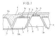
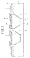
- Fig. 1 shows a sectional view of a hybrid integrated circuit device according to Fig. 1 being not covered by the claims
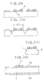
- Figs. 2(a) to (j) show sectional views illustrating its production process.
- reference numeral 1 shows a semiconductor chip which is comprised of a silicon substrate having a face-orientation (100).
- a taper portion 8 is formed on the upper-end face by anisotropic etching.
- Reference numeral 2 shows an adhesive member (e.g. low-boiling point glass, resin such as polyimide and epoxy, and, eutectic).
- Reference numeral 3 shows a silicon substrate having a face-orientation of (100).
- a chip-coupling hole 3a is formed on the opposite side of the substrate by anisotropic etching so that its size is the same as that of the semiconductor chip 1.
- the surface of the semiconductor chip 1 does not correspond to that of the substrate 3. Since it is difficult to connect the semiconductor chip 1 to the substrate 3 by film wiring in such a case, or if the surface of the semiconductor chip 1 does not protrude upwardly from the surface of the substrate 3, it is necessary to take a measure so that the surface of the semiconductor chip 1 is no lower than that of the substrate 3.
- the device is supposed to be designed so that the surface of the semiconductor chip 1 corresponds to that of the substrate 3 when the thickness of the substrate 3 is the maximum (when the disperison is +At). So the maximum gap which might occur between the semiconductor chip 1 and the substrate 3 would be 2 ⁇ t. Accordingly, for the purpose of making the semiconductor chip 1 stick up from the surface of the substrate 3, it is necessary to design it beforehand so as to make the surface of the semiconductor chip 1 stick up by 2 ⁇ t.
- the leveling layer 4 is formed across the semiconductor chip 1 and the substrate 3 so as to level the gap which has been occurred. Polyimide resin or SOG(spin on glass) is applied to the material of the leveling layer 4.
- Reference numeral 5 is wiring made of aluminum electrically connected to the semiconductor chip 1.
- Reference numeral 6 shows a passivation film of the semiconductor chip 1.
- Reference numeral 7a shows an electrode which is made of aluminum for instance and formed on the surface of the semiconductor chip 1'
- Reference numeral 7b shows an electrode which is formed on the surface of the substrate 3.
- Reference numeral 8 and 9 show taper portions which are formed by anistropic etching.
- Reference numeral 10a and 10b show a passivation film of the substrate 3.
- Reference numeral 11 shows a position-indication-hole for indicating the relationship between the main surface of the substrate 3 and the opposite side of the substrate 3.
- the semiconductor chip 1 and the substrate 3 include other elements such as transistors and resistances which are not illustrated in the drawings and electrically connected to the electrodes 7a and 7b, and wiring 5.
- electrode 7a is formed on the semiconductor chip 1 after the elements such as transistors and resistances have been formed on the semiconductor chip 1 by conventional process such as impurity doping.
- the passivation film 6 of nitride silicon is formed on the semiconductor chip 1 as shown in Fig. 2(a).
- a V shape ditch is formed by anisotropic etching which uses the partially opened passivation film 6 as a mask.
- the angle "A" of the V shape ditch is approximately 54.7°. Since the surface of the V shape ditch becomes a contacting surface, it is necessary to form it deeply in order to improve the coupling strength.
- the semiconductor chip 1 is cut along the V shape ditch as shown in Fig. 2(c) to obtain a unit chip.
- both sides of the substrate 3 are covered with passivation films 10a and 10b as shown in Fig. 2(d) after the electrode 7b has been formed on the substrate 3.
- the position-indication hole 11 is formed as shown in Fig. 2(e) by anisotropic etching which uses the partially opened passivation film 10a as a mask.
- the difference between the position of the electrode 7b and the back side of the substrate 3 is clarified by the presence of the position-indication-hole 11.
- the passivation film 10b is etched with reference to the position of the position-indication hole 11 as shown in Fig. 2(f).
- the chip-coupling hole 3a is formed by anisotropic etching which uses the partially opened passivation film 10b as a mask as shown in Fig. 2(g).
- the angle "B" between the taper portion and the main surface of the substrate 3 is set at about 54.7°.
- the length "L” is determined so that the surface length "L2" of the chip-coupling hole 3a.
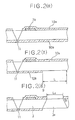
- the above processed semiconductor chip 1 is coupled to the above processed substrate 3 through the adhesive member 2 as shown in Fig. 2(h).
- the adhesive member 2 has to be treated with heat which has no adverse influence on the elements (e.g. below 500°C in case aluminum wiring is used in the elements).
- the adhesive member 2 has to withstand that heat-treatment in the next process for forming the leveling layer 4 shown in Fig. 2(i).
- a polyimido resin is used as the leveling layer 4 and treated with the maximum temperature 350°C.
- a low-boiling point glass or polyimido resin is used in the adhesive member 2.
- a contact hole 12 is formed by O2 plasma etching for instance as shown in Fig. 2(j).
- aluminum film is formed by vapor deposition or sputtering. This aluminum film is etched in a pattern that forms the wiring 5 which connects the electrode 7a on the semiconductor chip 1 to the electrode 7b on the substrate 3. Even if the above-described leveling is insufficient, disconnection of the wiring 5 can be prevented because the gap portion has a taper angle of 125° and the chip surface protrudes upwardly from the surface of the substrate 3.
- the semiconductor chip 1 and the substrate 3 have taper portions 8 and 9, respectively, and they are coupled to each other so that each taper portion corresponds to each other. So the accuracy of the chip position in the horizontal direction can be improved since the tapered portion 8 is couple to the tapered portion 9 through the adhesive member 2 with a rubbing movement. Both taper portions 8 and 9 are accurately formed by anisotropic etching. In the etching process of the silicon having the face orientation (100), since the etching mask has an square opening, its etching proceeds with exposing an equivalent face along the square opening. As a result, all taper angles of the tapered portions are the same angle (54.7°) and taper portion 8 becomes parallel to the taper portion 9.
- the taper portion 9 of the semiconductor chip 1 is formed in its back side by anisotropic etching, and the taper portion 8 of the substrate 3 is formed in its main surface in the same etching technique.
- the taper portion 9 is coupled to the taper portion 8 by the self-aignment coupling.
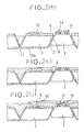
- the chip-coupling hole 3a of the second example is not a through-hole. According to the second example, since the depth and the interval of the semiconductor chip 1 can be determined independently of the substrate 3, further high-density integration can be obtained. However, as the semiconductor chip 1 protrudes upwardly from the surface of the substrate 3 corresponding to its depth, such protruding portion has to be leveled by a polyimido resin layer 4.
- a third example not being covered by the claims is explained with reference to Fig. 4.
- Most of the structures of the third example are the same as those of the first example.
- a plurality of semiconductor chips 1 are connected to one another by wiring 5 while in the first example the semiconductor chips 1 is connected to the substrate 3 by wiring 5.
- the reference numerals identical to those of the first examples denote the same elements as those of the first example. It is obvious that such elements have the same effect as those in the first example.
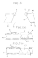
- FIG. 5 illustrates the basic structure of the present invention.
- Fig. 6 illustrates a characteristic portion of the present embodiment, namely the sectional view of a hole formed in a wiring-substrate 40.
- Figs. 7(a) and (b) show a process of the hole shown in Fig. 6.
- a substrate 20 is a flat board such as silicon wafer, ceramic board, metal board or glass board.
- Reference numeral 30 designates a semiconductor chip made of silicon having the face-orientation (100).
- a taper portion 31 is formed on the upper part of the semiconductor chip 30 by anisotropic etching (alkali solvent).
- Reference numeral 40 denotes a silicon substrate which has the face-orientation (100). This silicon substrate 40 is used for forming wiring.
- Reference numeral 50 denotes an adhesive member for coupling the semiconductor chip and the substrate 40 with a flat substrate 20 (e.g., low-boiling-point glass or polyimide resin, etc.).
- Reference numeral 41 denotes a coupling-hole, which is formed by anisoropic etching.
- the coupling hole 41 has a first taper portion 43 formed on a main surface 42 as indicated by a circle A in Fig. 6 and a second taper portion 45 formed in the substrate 40. So the opening area of the inside of the coupling hole 41 is smaller than that on the main surface of the substrate 40, and the opening area of the inside of the coupling-hole 41 is smaller than that on the opposite side 44 of the substrate 40.
- reference numerals 60 and 70 designate electrodes
- 80 and 90 designate a leveling layer and wiring, respectively.
- Fig. 7 illustrates the process for manufacturing the coupling hole 41.
- L1, ts, and ⁇ t designate the length of the upper-plain portion of the semiconductor chip 30, a thickness of the substrate 40 and an unevenness, respectively.
- Designation ⁇ indicates an angle (54.7° to silicon (100)) of a taper which is formed in an anisotropic etching.
- etching mask films 46 and 47 made of SiO2 or Si3N4 are formed on opposite sides of the substrate 40 so as to form a tapered hole 41a in size B. Then, as shown in Fig. 7(b), the etching mask film 47 on the opposite side of the substrate 40 has etched a tapered hole 41b in the length C by anisotropic etching. In this process, both etching mask films 46 and 47 may be etched by anisotropic etching at the same time.
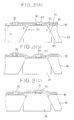
- Figs. 8(a)-(c) By using the above described structure in the tapered hole 41b, the laterprocesses shown in Figs. 8(a)-(c) can be obtained irrespective of the thickness of the semiconductor chip 30.
- Fig. 8(a), Fig. 8(b) and Fig. 8(c) show a case in which the thickness of the semiconductor chip 30 equals that of the substrate 40, and a case in which the semiconductor chip 30 is thinner than the substrate 50, respectively.
- the gap which occurs at a coupling portion when the taper portion of the semiconductor chip 30 is coupled to the taper hole of the substrate 40 may be absorbed by the adhesive member 50 using other material such asresin (i.e., an adhesive which is hardened by a heat treatment).
- an angle "D" formed between the main surface 42 of the substrate 40 and the first taper portion 43 always becomes an obtuse angle regardless of the presence of the gap which occurs due to the uneveness between the thickness of the semiconductor chip 30 and that of the substrate 40, because the first tapered portion 43 is formed in the coupling hole 41 in addition to the second taper portion 45.
- a portion above the first tapered portion 43 becomes a gentle surface as shown in Fig. 8(b) so that disconnection of wiring 90 can be prevented effectively.
- the present invention can be applied to a semiconductor device using a semiconductor chip which is directly coupled to a substrate, and is especially effective in being applied to a high-density integrated circuit or a semiconductor device in which a material of the semiconductor chip differs from that of the substrate.
Landscapes
- Wire Bonding (AREA)
- Internal Circuitry In Semiconductor Integrated Circuit Devices (AREA)
Claims (4)
- Halbleitervorrichtung, welche aufweist:
ein aus einem Halbleiterkristallmaterial hergestelltes Substrat (40) mit einer vorbestimmten Kristallorientierung, in welchem eine Kopplungsöffnung (41) derart ausgebildet ist, daß die Kopplungsöffnung (41) durch das Substrat (40) ausgehend von einer Hauptseitenoberfläche (42) des Substrates (40) bis zu einer entgegengesetzten Seitenoberfläche (44) des Substrates (40) angeordnet ist, wobei eine Öffnungsgröße (C) der Kopplungsöffnung (41) bei der entgegengesetzten Seitenoberfläche (44) größer ist als eine Öffnungsgröße (B) der Kopplungsöffnung (41) bei der Kauptseitenoberfläche (42); wobei die Kopplungsöffnung (41) einen ersten, sich verjüngenden Abschnitt (43) aufweist, der auf der Hauptoberfläche (42) des Substrates (40) derart ausgebildet ist, daß die Fläche der Öffnungsgröße (B) der Kopplungsöffnung (41) bei der Hauptoberfläche des Substrates (40) größer ist als eine Fläche eines inneren Abschnittes des Substrates (40), und einen zweiten, sich verjüngenden Abschnitt (45) aufweist, der auf der entgegengesetzten Seite (44) der Hauptoberfläche (42) des Substrates (40) derart ausgebildet ist, daß die Fläche der Öffnungsgröße (C) der Kopplungsöffnung (41) der entgegengesetzten Seitenoberfläche (44) größer ist als die Fläche des inneren Abschnitt des Substrates (40);
einen Halbleiterchip (30), der aus einem Halbleiterkristallmaterial hergestellt ist und einen sich verjüngenden Abschnitt (31) mit einer Form derart aufweist, daß der Halbleiterchip (30) paßgenau in der Kopplungsöffnung (41) des Substrates (40) anordenbar ist;
ein Kopplungsteil (50) zum Koppeln des Kalbleiterchip (30) an das Substrat (40) derart, daß sich der zweite, sich verjüngende Abschnitt (45) des Substrates (40) und der sich verjüngende Abschnitt (31) des Halbleiterchips (30) gegenseitig entsprechen;
eine Nivellierschicht (80), welche über das Substrat (40) und den Halbleiterchip (30) gebildet ist;
eine Verdrahtung (90), die elektrisch mit einem auf dem Halbleiterchip (30) gebildeten Element verbunden ist, wobei zumindest ein Teil der Verdrahtung (90) auf der Nivellierschicht (80) gebildet ist. - Halbleitervorrichtung nach Anspruch 1, bei dem die Hauptseitenoberfläche des Halbleiterchips (30) sich nach oben von der Hauptseitenoberfläche (42) des Substrates (40) erhebt.
- Halbleitervorrichtung nach Anspruch 1 oder 2, bei dem das Substrat (40) und der Halbleiterchip (30) aus Silizium hergestellt sind.
- Halbleitervorrichtung nach einem der vorhergehenden Ansprüche, bei dem der Halbleiterchip (30) dieselbe Kristallorientierung wie das Substrat (40) aufweist.
Applications Claiming Priority (2)
| Application Number | Priority Date | Filing Date | Title |
|---|---|---|---|
| JP18419188 | 1988-07-22 | ||
| JP184191/88 | 1988-07-22 |
Publications (3)
| Publication Number | Publication Date |
|---|---|
| EP0448713A4 EP0448713A4 (de) | 1991-07-09 |
| EP0448713A1 EP0448713A1 (de) | 1991-10-02 |
| EP0448713B1 true EP0448713B1 (de) | 1993-10-27 |
Family
ID=16148949
Family Applications (1)
| Application Number | Title | Priority Date | Filing Date |
|---|---|---|---|
| EP89908519A Expired - Lifetime EP0448713B1 (de) | 1988-07-22 | 1989-07-21 | Halbleiteranordnung |
Country Status (4)
| Country | Link |
|---|---|
| US (1) | US5153700A (de) |
| EP (1) | EP0448713B1 (de) |
| DE (1) | DE68910327T2 (de) |
| WO (1) | WO1990001215A1 (de) |
Families Citing this family (7)
| Publication number | Priority date | Publication date | Assignee | Title |
|---|---|---|---|---|
| WO2001075789A1 (en) * | 2000-04-04 | 2001-10-11 | Toray Engineering Company, Limited | Method of manufacturing cof package |
| JP4198966B2 (ja) * | 2002-10-17 | 2008-12-17 | 株式会社東芝 | 半導体装置の製造方法 |
| US7405787B2 (en) | 2003-03-25 | 2008-07-29 | Nitto Denko Corporation | Liquid crystal display with offset viewing cone |
| EP1517166B1 (de) | 2003-09-15 | 2015-10-21 | Nuvotronics, LLC | Vorrichtungsgehäuse und Verfahren zu derer Prüfung und Herstellung |
| DK1962344T3 (da) | 2007-02-25 | 2012-07-02 | Samsung Electronics Co Ltd | Emballager til elektroniske indretninger og fremgangsmåder til fremstilling |
| US10319654B1 (en) | 2017-12-01 | 2019-06-11 | Cubic Corporation | Integrated chip scale packages |
| US10692804B2 (en) * | 2018-08-15 | 2020-06-23 | Advanced Semiconductor Engineering, Inc. | Semiconductor device package and method of manufacturing the same |
Citations (2)
| Publication number | Priority date | Publication date | Assignee | Title |
|---|---|---|---|---|
| JPS5756216B2 (de) * | 1979-01-12 | 1982-11-29 | ||
| JPS5853847A (ja) * | 1981-09-25 | 1983-03-30 | Fujitsu Ltd | 超高周波モジュ−ル |
Family Cites Families (8)
| Publication number | Priority date | Publication date | Assignee | Title |
|---|---|---|---|---|
| US3871015A (en) * | 1969-08-14 | 1975-03-11 | Ibm | Flip chip module with non-uniform connector joints |
| JPS5321771A (en) * | 1976-08-11 | 1978-02-28 | Sharp Kk | Electronic parts mounting structure |
| JPS6059857B2 (ja) * | 1980-09-22 | 1985-12-27 | 横浜ゴム株式会社 | 柔軟性を有する帯状材料の貼り合せ方法及び装置 |
| US4670770A (en) * | 1984-02-21 | 1987-06-02 | American Telephone And Telegraph Company | Integrated circuit chip-and-substrate assembly |
| EP0172889A1 (de) * | 1984-02-17 | 1986-03-05 | AT&T Corp. | Zusammenbau mit integriertem schaltungschip |
| JPS62147746A (ja) * | 1985-12-20 | 1987-07-01 | Nec Corp | 集積回路構造 |
| JPS62291037A (ja) * | 1986-06-10 | 1987-12-17 | Oki Electric Ind Co Ltd | 半導体チツプのダイボンデイング方法 |
| JPS63156328A (ja) * | 1986-12-19 | 1988-06-29 | Ricoh Co Ltd | 集積回路装置チツプの実装体 |
-
1989
- 1989-07-21 WO PCT/JP1989/000730 patent/WO1990001215A1/ja not_active Ceased
- 1989-07-21 EP EP89908519A patent/EP0448713B1/de not_active Expired - Lifetime
- 1989-07-21 DE DE68910327T patent/DE68910327T2/de not_active Expired - Fee Related
-
1991
- 1991-01-22 US US07/643,585 patent/US5153700A/en not_active Expired - Fee Related
Patent Citations (2)
| Publication number | Priority date | Publication date | Assignee | Title |
|---|---|---|---|---|
| JPS5756216B2 (de) * | 1979-01-12 | 1982-11-29 | ||
| JPS5853847A (ja) * | 1981-09-25 | 1983-03-30 | Fujitsu Ltd | 超高周波モジュ−ル |
Also Published As
| Publication number | Publication date |
|---|---|
| US5153700A (en) | 1992-10-06 |
| DE68910327T2 (de) | 1994-05-19 |
| DE68910327D1 (de) | 1993-12-02 |
| EP0448713A1 (de) | 1991-10-02 |
| EP0448713A4 (de) | 1991-07-09 |
| WO1990001215A1 (fr) | 1990-02-08 |
Similar Documents
| Publication | Publication Date | Title |
|---|---|---|
| US5237130A (en) | Flip chip technology using electrically conductive polymers and dielectrics | |
| US6138348A (en) | Method of forming electrically conductive polymer interconnects on electrical substrates | |
| KR100595885B1 (ko) | 반도체장치 및 그 제조방법 | |
| US8063493B2 (en) | Semiconductor device assemblies and packages | |
| EP1030369B1 (de) | Mehrchipmodulstruktur und seine herstellung | |
| KR100290193B1 (ko) | 반도체장치및그제조방법 | |
| US10446515B2 (en) | Semiconductor substrate and semiconductor packaging device, and method for forming the same | |
| US20080036061A1 (en) | Integrated chip carrier with compliant interconnect | |
| TWI605557B (zh) | 電子封裝件及其製法與基板結構 | |
| US5406122A (en) | Microelectronic circuit structure including conductor bridges encapsulated in inorganic dielectric passivation layer | |
| EP0448713B1 (de) | Halbleiteranordnung | |
| US7205181B1 (en) | Method of forming hermetic wafer scale integrated circuit structure | |
| KR101266642B1 (ko) | 집적 회로 및 본드 패드 형성 방법 | |
| US6107179A (en) | Integrated flexible interconnection | |
| TWI604588B (zh) | 封裝結構及其製造方法 | |
| JPH0410635A (ja) | フリップチップ実装方法 | |
| JP2815650B2 (ja) | 半導体装置 | |
| JPH10209164A (ja) | 半導体装置の製造方法 | |
| US20090001597A1 (en) | Semiconductor device having an interconnect electrically connecting a front and backside thereof and a method of manufacture therefor | |
| US6560735B1 (en) | Methods and apparatus for testing integrated circuits | |
| KR0160959B1 (ko) | 상호접속 구조물 | |
| CN120784169A (zh) | 基板处理方法及半导体装置 | |
| JPWO1990001215A1 (ja) | 半導体装置 | |
| CN120652608A (zh) | 具有扩展金属层的光子器件和方法 | |
| JPH04250628A (ja) | 半導体装置の製造方法 |
Legal Events
| Date | Code | Title | Description |
|---|---|---|---|
| PUAI | Public reference made under article 153(3) epc to a published international application that has entered the european phase |
Free format text: ORIGINAL CODE: 0009012 |
|
| 17P | Request for examination filed |
Effective date: 19910121 |
|
| AK | Designated contracting states |
Kind code of ref document: A1 Designated state(s): DE |
|
| 17Q | First examination report despatched |
Effective date: 19920615 |
|
| GRAA | (expected) grant |
Free format text: ORIGINAL CODE: 0009210 |
|
| AK | Designated contracting states |
Kind code of ref document: B1 Designated state(s): DE |
|
| REF | Corresponds to: |
Ref document number: 68910327 Country of ref document: DE Date of ref document: 19931202 |
|
| PLBE | No opposition filed within time limit |
Free format text: ORIGINAL CODE: 0009261 |
|
| STAA | Information on the status of an ep patent application or granted ep patent |
Free format text: STATUS: NO OPPOSITION FILED WITHIN TIME LIMIT |
|
| 26N | No opposition filed | ||
| PGFP | Annual fee paid to national office [announced via postgrant information from national office to epo] |
Ref country code: DE Payment date: 20010716 Year of fee payment: 13 |
|
| PG25 | Lapsed in a contracting state [announced via postgrant information from national office to epo] |
Ref country code: DE Free format text: LAPSE BECAUSE OF NON-PAYMENT OF DUE FEES Effective date: 20030201 |