EP0448470B1 - Appareil de traitement d'images ayant la capacité de réduction d'images et procédé correspondant - Google Patents
Appareil de traitement d'images ayant la capacité de réduction d'images et procédé correspondant Download PDFInfo
- Publication number
- EP0448470B1 EP0448470B1 EP91400758A EP91400758A EP0448470B1 EP 0448470 B1 EP0448470 B1 EP 0448470B1 EP 91400758 A EP91400758 A EP 91400758A EP 91400758 A EP91400758 A EP 91400758A EP 0448470 B1 EP0448470 B1 EP 0448470B1
- Authority
- EP
- European Patent Office
- Prior art keywords
- curtailment
- image
- line
- image processing
- processing apparatus
- Prior art date
- Legal status (The legal status is an assumption and is not a legal conclusion. Google has not performed a legal analysis and makes no representation as to the accuracy of the status listed.)
- Expired - Lifetime
Links
Images


Classifications
-
- H—ELECTRICITY
- H04—ELECTRIC COMMUNICATION TECHNIQUE
- H04N—PICTORIAL COMMUNICATION, e.g. TELEVISION
- H04N1/00—Scanning, transmission or reproduction of documents or the like, e.g. facsimile transmission; Details thereof
- H04N1/387—Composing, repositioning or otherwise geometrically modifying originals
- H04N1/393—Enlarging or reducing
- H04N1/3935—Enlarging or reducing with modification of image resolution, i.e. determining the values of picture elements at new relative positions
Definitions
- This invention relates to an image processing apparatus which processes a binarized pixel image data of M pixels in the row or line scanning direction and N pixels in the column or paper feeding direction so as to reduce to binarized pixel image data of m pixels in the row direction and n pixels in the column direction.
- an image may be reduced by curtailment of pixels in each line in a main scanning direction and curtailment of lines in a sub-scanning direction, because the display apparatus does not have a display area or the capability to print on a sheet of proper size, e.g., see Japanese Laid-open Patents JP-A-58125953 and JP-A-60132273 and United States Patent US-A-4,536,802. Special processing is required to output a reduced image onto the display screen or sheet.
- a sending facsimile apparatus has an image reading unit which is capable of reading an image with high resolution and a receiving facsimile appparatus has a printing unit which can only output the image data using lower resolution than the sending facsimile apparatus.
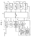
- FIG. 1 is a block diagram of a facsimile apparatus including an image processing apparatus according to the present invention.
- the facsimile apparatus includes an image reading unit 10, illustrated in more detail in FIG. 2, for reading image data from an original document.
- a data compression/decompression unit 12 compresses the image data read by the image reading unit 10 and decompresses image data received from another facsimile apparatus (not shown) connected by a phone line 13.
- the phone line 13 is connected to an interface control unit 14 in the facsimile apparatus illustrated in Fig. 1.
- a modem 16 connected to the interface control unit 14 transmits and receives over the phone line 13.
- the image reducing unit 24 is provided for reducing the image data.
- a main control unit 26 controls the operation of the facsimile apparatus illustrated in FIG. 1 in response to instructions received from an operator panel unit 28.
- the image reducing unit 24 includes a curtailment pattern generating circuit 30, a curtailment position setting circuit 32, and a data conversion circuit 34. The operation of the circuits in the image reducing unit 24 will be described below with reference to FIG. 4.
- FIG. 2 is a block diagram of the detailed structure of the image reading unit 10.
- a document 40 is fed along a subscanning direction, indicated by arrow Y in FIG. 2, by rollers 42a and 42b.
- a motor 44 is controlled via a driving unit 45 by main control unit 26 to rotate the rollers 42.
- An image on the document 40 is read by a charge coupled device (CCD) unit 46 using a focusing lens 48.
- the CCD unit 46 is driven by a driving unit 50 which is controlled by the main control unit 26.
- the CCD unit 46 includes about 5000 or more CCD devices which are arranged in a main scanning direction, indicated by arrow X in FIG.2, to read an A3 size document with a resolution of 400 dpi.
- the CCD unit 46 outputs an output signal, in accordance with the density of an image on the document 40, to a multi-value image data producing unit 52.
- the multi-value image data producing unit 52 produces 16 levels per pixel by comparing the output signal from the CCD unit 46 with predetermined multi-threshold levels and then the multi-value image data is output to a dither/binarizer 54. Namely, where an image on the document 40 includes a half-tone image, the output signal from the CCD unit 46 supplies multi-level or analog values continuously varying from a minimum level to a maximum level.
- the dither/binarizer 54 converts the multi-value image data from the image data producing unit 52 to binarized pixel data using a dither method, etc.
- the binarized pixel data is stored in the image memory 20 under control of the main control unit 26. This procedure is used because the output apparatus, such as an electrophotographic or thermal printer which is typically used for printing in a facsimile apparatus, is unable to express a half-tone by one pixel. Hence, the half-tone image is converted to binarized pixel data by the dither method, etc.
- FIG. 3 is a block diagram illustrating the detailed structure of the printing unit 18.
- the printing unit 18 includes a printing controller 60 and a printing mechanism 62. Under control of the printing controller 60, the printing mechanism 62 prints out the binarized image data stored in the image memory 20 in accordance with instructions from the main control unit 26.
- the printing mechanism 62 may be an electrophotographic type printer which includes a photoconductive drum 64, a precharger 66, an exposure unit 68, a developing unit 70, a transfer charger 72, a cleaner 74, a heat roller type fuser 76, a stacker 78, two hoppers 80a and 80b for different size paper and two paper size detectors 82a and 82b which detect the size of the paper which is placed in each hopper 80a and 80b.
- the exposure unit 68 may be an LED array type, as illustrated in FIG. 3, or a mirror scanning type, or any conventional exposure unit. Detection signals of the paper size detectors 82a and 82b are output to the printing controller 60.
- a document 40 is first set in a reading position in the image reading unit 10.
- the size of the document 40 is detected by the photosensitive sensors 84a to 84c and a paper size detector 86 sends the paper size to the main control unit 26.
- the main control unit 26 controls the image reading unit 10 to read the document 40 and stores the binarized pixel data in the image memory 20. Namely, image data to be reduced is stored to the image memory 20 as a binarized pixel data so that cost of the image memory 20 is minimal. Then the main control unit 26 proceeds with the sending procedure to another (receiving) facsimile apparatus.
- the main control unit 26 After the main control unit 26 receives information from the receiving facsimile apparatus indicating the size of the recording sheet, resolution of the print unit, etc., the main control unit 26 determines a curtailment rate in accordance with the size of document reported by the paper size detector 86 and the recording sheet size or the resolution from the receiving facsimile apparatus.
- the receiving facsimile apparatus determines the size of the recording sheet using a paper size detector like detectors 82a, 82b shown in FIG. 3, if the receiving facsimile apparatus has the same printing unit shown in FIG. 3.
- the printing controller 60 transmits the size of the recording sheet which is detected by the sensors 82a and 82b to the main control unit in the receiving facsimile apparatus. Then the main control unit in the receiving facsimile apparatus sends the size of the recording sheet to the sending facsimile apparatus.
- the main control unit 26 in the sending facsimile apparatus calculates a curtailment rate and operates the image reducing unit 24 in compliance with the curtailment rate.
- the binarized pixel data to be sent from the image memory 20, which is B4 size image.data is reduced to A4 size binarized pixel data by the image reducing unit 24.
- The, e.g., A4 size pixel data is compressed by the data compression/decompression unit 12 and is transmitted to the receiving facsimile apparatus through the modem 16, the interface control unit 14, and the phone line 13 under control of the main control unit 26. Finally, the binarized pixel data is printed out by the printing unit in the receiving facsimile apparatus.
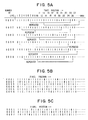
- the curtailment pattern generating circuit 30 comprises a read only memory (ROM) 90 which stores a curtailment pattern as shown in FIGS. 5A-5C, an address generating circuit 92 and a data register 94.
- FIG. 5A shows a curtailment pattern for reducing A3 size pixel data to B4 size pixel data
- FIG. 5B is a pattern for converting B4 to A4
- FIG. 5C is a pattern for converting A3 to A4.
- CITT Consultative Committee for International Telephone and Telephone
- the curtailment rate is 16/19; B4 to A4 is 27/32; and A3 to A4 is 27/38.
- the 16/19 rate because 19 pixels are reduced to 16 pixels, one pixel is eliminated for each 6.33 pixels. Namely, the sixth pixel, the thirteenth pixel (seventh pixel after the sixth pixel), the nineteenth pixel (sixth pixel after the thirteenth pixel) are eliminated in the 19 pixels and these curtailment positions are set to be repeated for each line of the main scanning direction. This is a 6-7-6 interval.
- the curtailment positions in the 27/32 rate are the sixth pixel, the thirteenth pixel (seventh pixel after the sixth pixel), the nineteenth pixel (sixth pixel after the thirteenth pixel, the twenty-sixth pixel (seventh pixel after the nineteenth pixel), and the thirty-second pixel (sixth pixel after the twenty-sixth pixel) in the thirty-two pixels, and each curtailment position is set to be repeated in each line. This is a 6-7-6-7-6 interval.
- the curtailment positions in the 27/38 rate are the third pixel, the seventh pixel (fourth pixel after the third pixel), the tenth pixel, the fourteenth pixel, the seventeenth pixel, twentieth pixel, the twenty-fourth pixel, the twenty-seventh pixel, the thirty-first pixel, the thirty-fifth pixel, and the thirty-eighth pixel in the thirty-eight pixels, and each curtailment position is set to be repeated in each line. This is a 3-4-3-4-3-4-3-4-3-4-3-4-3 interval.
- a data "0" in a pixel position indicates a curtailment position and a data "1" in a pixel indicates a writing or noncurtailment position.
- the curtailment positions on adjacent lines are different. Namely, in FIGS. 5A and 5B, the first curtailment position occurs at six different pixels in the six lines of the curtailment pattern. Thereby, all of the curtailment positions differ in the lines in the curtailment pattern.
- each line of the curtailment pattern has a different first curtailment position within the first three pixels. Thereby, all of the curtailment positions are different on the three lines in the curtailment pattern.
- FIGs. 5A-5C illustrate curtailment where resolution is the same and the size of the document is reduced.
- the curtailment rate is calculated based upon resolution before and after curtailment, for example, 400 dpi to 300 dpi is 3/4.
- curtailment lines in the subscanning direction which is the paper feeding direction are decided in the same manner as curtailment in the main scanning direction and thus, lines are reduced in a manner similar to that described above.
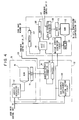
- the curtailment position setting circuit 32 comprises a parallel/serial conversion circuit 96, a buffer memory 98 such as a FIFO memory, and a subscanning curtailment position setting circuit 100.
- the data conversion circuit 34 comprises a buffer memory 102 such as a FIFO memory, a gate circuit 104 which may be a latch circuit, a buffer memory 106 such as a FIFO memory, a serial/parallel conversion circuit 108, a data register 110, a random access memory (RAM) 112, an address register 114, and a writing address generating circuit 116.
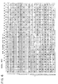
- FIGs. 5-8 illustrate a curtailment rate of 16/19 in which A3 size paper is reduced to B4 size.
- binarized pixel data which is stored in the image memory 20 is read out arid then stored in the buffer memory 102.
- the main control unit 26 outputs a select signal which indicates a curtailment rate to the curtailment pattern generating circuit 30 and the curtailment position setting circuit 32.
- the address generating circuit 92 in the curtailment pattern generating circuit 30 generates an address to read out a curtailment pattern, for the curtailment rate 16/19 as shown in FIG. 5A, from the ROM 90.
- Curtailment pattern data for example, the 8 bits of data, "11111011", which are the first 8 bits of line number 1 in FIG. 5A, are output from ROM 90 to the data register 94.
- the 8 bits of curtailment pattern data received from ROM 90 are converted to serial data by the parallel/serial conversion circuit 96 in accordance with a converting signal from the main control unit 26.
- the serial data are sent to the buffer memory 98 under control of the main control unit 26 in synchronization with reading of the image data from the image memory 20.
- Output signals from the buffer memories 98 and 102 are input to the latch circuit 104. If the output signal of the buffer memory 90 is a "1", the latch circuit 104 outputs the input signal from the buffer memory 102 to the buffer memory 106. On the other hand, if the output signal of the buffer memory 98 is a "0", the latch circuit 104 inhibits output of the signal from the buffer memory 102 to the buffer memory 106.
- the first five binarized pixel data, "10001", in line number 1 in FIG. 6 will be stored in the buffer memory 106. Then the pixel data, "0", of sixth,pixel position in line number 1 in FIG. 6 is not stored in the buffer memory 106 and the line length is thereby reduced, because the sixth pixel position in buffer memory 98 is "0". Furthermore, the seventh and eighth pixel data in line number 1 in FIG. 6 are stored in the buffer memory 106 because the output signals of the seventh and eighth positions from the buffer memory 98 are "1".
- the output signals from the buffer memory 98 are supplied to the latch circuit 104, the output signals of the buffer memory 102 are supplied to the buffer memory 106 or are inhibited by the latch circuit 104 in accordance with the pattern data ("1" or "0") from the buffer memory 98.
- the data "100010001" which are the first nine pixel data in line number 1 in FIG. 6 are converted to the data "10001001".
- the serial data from buffer 106 are then converted to parallel data under control of a converting signal from the main control unit 26 after serial data of 8 bits have been input to the serial/parallel conversion circuit 108.
- the buffer memory 106 can store at least nine pixels of data
- the converting signal 118 controlling the serial/parallel conversion circuit 108 may be supplied by the main control unit 26 one cycle later than the converting signal 120 controlling the parallel/serial conversion circuit 96.
- the 8 bits of parallel data is stored in the RAM 112 (see the first 8 bits of line number 1 in FIG. 7) at an address which is set in the address register 114 by the writing address generating circuit 116.
- the writing address generating circuit 116 generates an address in compliance with the converting signal 118 after a necessary time has passed to process the operation of the serial/parallel conversion circuit 108.
- the address generating circuit 92 Prior to finishing the reducing process for line number 1 in the document 40, the address generating circuit 92 generates an address to read out the curtailment pattern for the line number 2.
- the same curtailment process described above is used for lines 2-5.
- the entire-sixth line of the binarized pixel data in the image memory 20 is deleted, under the control of the subscanning curtailment position setting circuit 100, which reduces the number of lines in the document 40 according to the curtailment rate.
- the subscanning curtailment position setting circuit 100 deletes the thirteenth line (seven lines past the sixth line), nineteenth line (six lines past the thirteenth line), the twenty-fifth line (six lines past the nineteenth line), etc.
- the address generating circuit 92 does not increment the address to read out a curtailment pattern for, e.g., the sixth line of the document 40 in compliance with a curtailment signal from the subscanning curtailment position setting circuit 100 and therefore, the ROM 90 outputs the fifth line of the curtailment pattern, even though the sixth line of the binarized pixel data in the image memory 20 is output to the buffer memory 102.
- the address generating circuit 92 increments the address and then the sixth line of the curtailment pattern is read out from the ROM 90 to apply for the seventh line of the binarized pixel image data read out from the image memory 20.
- the writing address generating circuit 116 does not increment the address register 114 to write to the RAM 112 in accordance with the curtailment signal from circuit 100.
- the data is overwritten in the RAM 112 so as to be added to data which has already been stored in the same address of the RAM 112 for the preceding line, e.g., line 5.
- the writing address generating circuit 116 increments the address register 114 to store the seventh line of the binarized pixel data at the address of the sixth line of the RAM 112.
- the binarized pixel data shown in FIG. 6 will be reduced by the reducing process of the present invention so that binarized pixels are reduced at the predetermined positions of the sixth, thirteenth, nineteenth, twenty-fifth, forty-fourth,... pixel in each line.
- periodical unevenness occurs in the reduced binarized pixel data as shown in FIG. 8. Namely, as shown in FIG. 8, a gap between two black pixels may be wider than a gap before curtailment, for example, the gap between the eighth and fifteenth pixels on line 1 is extended from three white pixels (see FIG. 6) to six white pixels (see FIG. 8) or a gap between the forty-second and forty-fifth pixels on line 29 is extended from one white pixel (see FIG. 6) to two white pixels (see FIG. 8). These gaps also occur on other lines. These gaps are therefore seen by a viewer as a continuing white line prolonging along the sub-scanning direction in Fig. 8.
Landscapes
- Engineering & Computer Science (AREA)
- Multimedia (AREA)
- Signal Processing (AREA)
- Editing Of Facsimile Originals (AREA)
- Image Processing (AREA)
- Controls And Circuits For Display Device (AREA)
Claims (18)
- Appareil de traitement d'image possédant un moyen (24) de réduction d'image qui sert à réduire des données d'image mises sous forme binaire de M pixels par ligne dans une première direction et de N lignes dans une deuxième direction en des données d'image mises sous forme binaire de m pixels par ligne dans la première direction et de n lignes dans la deuxième direction, où M > m et N > n, ledit appareil comprenant :
un moyen de désignation (30, 32) servant à désigner des positions de pixels de troncation dans chaque ligne des données d'image mises sous forme binaire et des positions de lignes de troncation dans les données d'image mises sous forme binaire, selon un taux de réduction d'image, et
un moyen de troncation (34) servant à éliminer des pixels de chaque ligne aux positions de pixels de troncation désignées et à éliminer des lignes aux positions de lignes de troncation désignées,
caractérisé en ce que le moyen de désignation est conçu pour décaler les positions de pixels de troncation entre lignes adjacentes selon une séquence prédéterminée. - Appareil de traitement d'image selon la revendication 1, comprenant en outre un moyen de conversion (52, 54) servant à convertir une image de façon à la faire passer de la forme de données d'image à plusieurs valeurs par pixel à la forme de données d'image mises sous forme binaire par pixel, avec M pixels par ligne dans la première direction et N lignes dans la deuxième direction.
- Appareil de traitement d'image selon la revendication 1 ou 2, comprenant en outre un moyen de décision (26) servant à décider de la valeur du taux de réduction d'image en fonction des tailles, ou formats, d'image des données d'image mises sous forme binaire avant et après la troncation.
- Appareil de traitement d'image selon l'une quelconque des revendications 1 à 3, où ledit moyen de désignation comprend :
une mémoire (90), fonctionnellement connectée audit moyen de troncation (34), qui mémorise une configuration de troncation afin de commander la troncation de chaque ligne à réduire par ledit moyen de troncation,
un moyen de lecture (26, 92, 100) servant à lire la configuration de troncation dans ladite mémoire en fonction du taux de réduction d'image. - Appareil de traitement d'image selon la revendication 4, où ladite mémoire (90) mémorise une configuration de troncation pour J lignes, J étant inférieur à N, et
où ledit moyen de lecture (26, 92, 100) lit à répétition la configuration de troncation pour chaque nouveau groupe de J lignes. - Appareil de traitement d'image selon la revendication 5, où ledit moyen de lecture (26, 92, 100) fait une pause dans la lecture de la configuration de troncation lorsque ledit moyen de désignation (30, 32) désigne une position de ligne de troncation.
- Appareil de traitement d'image selon l'une quelconque des revendications 1 à 6, comprenant en outre :
un moyen de sortie (14) servant à délivrer les données de pixels tronquées qui sont produites par ledit moyen de troncation. - Appareil de traitement d'image selon l'une quelconque des revendications 1 à 7, où ledit moyen de troncation (34) est conçu pour supprimer par troncation des lignes en écrasant une ligne adjacente pour chacune des lignes à supprimer par troncation.
- Appareil de traitement d'image selon l'une quelconque des revendications 1 à 8, comprenant en outre un moyen (10) de lecture de document servant à lire une feuille d'un document afin de produire des données de pixels mises sous forme binaire ayant M pixels dans la première direction et N lignes dans la deuxième direction.
- Appareil de traitement d'image selon la revendication 9, où ledit moyen de lecture de document (10) comprend un moyen de conversion (52, 54) servant à convertir une image en la faisant passer de la forme données d'image à plusieurs valeurs par pixel à la forme données d'image mises sous forme binaire par pixel, avec M pixels dans la première direction et N lignes dans la deuxième direction.
- Appareil de traitement d'image selon l'une quelconque des revendications 1 à 10, comprenant en outre une mémoire (20), fonctionnellement connectée audit moyen de troncation (34), afin de mémoriser des données de pixels mises sous forme binaire ayant M pixels par ligne dans la première direction et N lignes dans la deuxième direction.
- Appareil de traitement d'image selon l'une quelconque des revendications 1 à 11, comprenant en outre un moyen (26) servant à fournir le taux de réduction d'image audit moyen de désignation (24).
- Appareil de traitement d'image selon l'une quelconque des revendication 1 à 12, comprenant en outre un moyen d'émission (14, 16) servant à émettre les données d'image réduites à destination d'un autre appareil de traitement d'image.
- Appareil de traitement d'image selon l'une quelconque des revendications 1 à 12, où ledit appareil peut être connecté à un autre appareil de traitement d'image, et comprend en outre :
un moyen d'émission (14, 16) servant à émettre les données d'image mises sous forme binaire réduites à destination de l'autre appareil de traitement d'image ; et
un moyen de réception (14) servant à recevoir des données d'image mises sous forme binaire traitées de la part de l'autre appareil de traitement d'image. - Appareil de traitement selon la revendication 14,
où ledit moyen de réception (14) est destiné à recevoir en outre un format de document de sortie de la part de l'autre appareil de traitement d'image ;
où ledit moyen de lecture de document (10) est en outre conçu pour produire un format de document d'entrée,
où ledit moyen de désignation (30, 32) possède un moyen servant à mémoriser des groupes de configurations de pixels pouvant être sélectionnés en fonction du taux de réduction d'image, et
où ledit appareil de traitement d'image comprend en outre un moyen servant à calculer le taux de réduction d'image à partir des formats de document d'entrée et de sortie. - Procédé de traitement d'image comprenant les opérations suivantes :(a) fournir des données de pixels mises sous forme binaire ayant M pixels par ligne dans une première direction et N lignes dans une deuxième direction ;(b) désigner des position de pixels de troncation dans chaque ligne de données de pixels et des positions de lignes de troncation en fonction d'un taux de réduction d'image ;(c) tronquer les données de pixels mises sous forme binaire qui sont fournies dans l'opération (a) afin de réduire celles-ci de M pixels par ligne et N lignes à des données de pixels mises sous forme binaire tronquées ayant m pixels par ligne dans la première direction et n lignes dans la deuxième direction en fonction des positions de pixels de troncation et des positions de lignes de troncation, où M > m et N > n ; et(d) délivrer les données de pixels mises sous forme binaire tronquées qui sont obtenues en résultat de l'opération (c) ;caractérisé en ce que la désignation de positions de troncation à l'opération (b) est faite de façon à provoquer un décalage des positions de pixels de troncation entre lignes adjacentes selon une séquence prédéterminée.
- Procédé de traitement d'image selon la revendication 16, où la troncation des lignes s'effectue par écrasement d'une ligne adjacente pour chacune des lignes devant être supprimées dans la troncation.
- Procédé de traitement d'image selon l'une quelconque des revendications 16 et 17, comprenant en outre les opérations suivantes :
incrémenter une ligne de sortie des données de pixels mises sous forme binaire tronquées correspondant à une ligne d'entrée des données de pixels mises sous forme binaire, et
interdire l'incrémentation de ladite ligne de sortie lorsque ladite désignation effectuée à l'opération (b) indique que la ligne d'entrée correspondante doit être supprimée dans la troncation, les pixels présents sur la ligne d'entrée étant écrits sur la ligne de sortie qui correspond à une ligne d'entrée immédiatement précédente.
Applications Claiming Priority (2)
| Application Number | Priority Date | Filing Date | Title |
|---|---|---|---|
| JP2070072A JPH03269775A (ja) | 1990-03-20 | 1990-03-20 | 画像縮小方式 |
| JP70072/90 | 1990-03-20 |
Publications (3)
| Publication Number | Publication Date |
|---|---|
| EP0448470A2 EP0448470A2 (fr) | 1991-09-25 |
| EP0448470A3 EP0448470A3 (en) | 1992-01-02 |
| EP0448470B1 true EP0448470B1 (fr) | 1995-12-06 |
Family
ID=13420974
Family Applications (1)
| Application Number | Title | Priority Date | Filing Date |
|---|---|---|---|
| EP91400758A Expired - Lifetime EP0448470B1 (fr) | 1990-03-20 | 1991-03-20 | Appareil de traitement d'images ayant la capacité de réduction d'images et procédé correspondant |
Country Status (4)
| Country | Link |
|---|---|
| EP (1) | EP0448470B1 (fr) |
| JP (1) | JPH03269775A (fr) |
| KR (1) | KR940007681B1 (fr) |
| DE (1) | DE69115089T2 (fr) |
Family Cites Families (6)
| Publication number | Priority date | Publication date | Assignee | Title |
|---|---|---|---|---|
| JPS5797271A (en) * | 1980-12-08 | 1982-06-16 | Ricoh Co Ltd | Thinning out and shrinking system and device for facsimile device |
| GB2100089B (en) * | 1981-05-28 | 1985-11-27 | Eltra Corp | Facsimile system with reduction of line spacing error |
| JPS58119259A (ja) * | 1982-01-08 | 1983-07-15 | Fuji Xerox Co Ltd | フアクシミリ装置 |
| JPS61210764A (ja) * | 1985-03-15 | 1986-09-18 | Fuji Xerox Co Ltd | フアクシミリ通信装置 |
| JPS63233670A (ja) * | 1987-03-20 | 1988-09-29 | Canon Inc | 画像信号処理装置 |
| JP2687366B2 (ja) * | 1987-09-18 | 1997-12-08 | 富士ゼロックス株式会社 | 画像読取装置 |
-
1990
- 1990-03-20 JP JP2070072A patent/JPH03269775A/ja active Pending
-
1991
- 1991-03-20 KR KR1019910004411A patent/KR940007681B1/ko not_active IP Right Cessation
- 1991-03-20 EP EP91400758A patent/EP0448470B1/fr not_active Expired - Lifetime
- 1991-03-20 DE DE69115089T patent/DE69115089T2/de not_active Expired - Fee Related
Also Published As
| Publication number | Publication date |
|---|---|
| DE69115089T2 (de) | 1996-04-25 |
| KR940007681B1 (ko) | 1994-08-22 |
| KR910017860A (ko) | 1991-11-05 |
| DE69115089D1 (de) | 1996-01-18 |
| EP0448470A3 (en) | 1992-01-02 |
| JPH03269775A (ja) | 1991-12-02 |
| EP0448470A2 (fr) | 1991-09-25 |
Similar Documents
| Publication | Publication Date | Title |
|---|---|---|
| JP3301607B2 (ja) | 画像処理装置 | |
| EP0827332A2 (fr) | Appareil et procédé de modification du rapport d'agrandissement ou de la réduction d'une image | |
| EP0601735B1 (fr) | Conversion de la résolution avec gris simulés par plusieurs bits | |
| US6088138A (en) | Image forming apparatus containing a display showing an adjustable image | |
| US5493415A (en) | Imgae processing system | |
| US6529287B1 (en) | Image processing system | |
| US4905095A (en) | Image processing apparatus | |
| US5517319A (en) | Apparatus for combining divided portions of larger image into a combined image | |
| JPH0937028A (ja) | 画像処理装置 | |
| US5647026A (en) | Uniformity correction and threshold or halftoning conversion unit and method | |
| JPH09130577A (ja) | 画像形成装置 | |
| JP3332398B2 (ja) | 画像処理装置及び画像処理方法 | |
| US5058038A (en) | Method to connect wide size scanner to laser printer engine for copying with size reduction | |
| US7016086B2 (en) | Image forming apparatus | |
| EP0395405B1 (fr) | Système de traitement d'images | |
| US6160249A (en) | Adaptive resolution scanning | |
| EP0448470B1 (fr) | Appareil de traitement d'images ayant la capacité de réduction d'images et procédé correspondant | |
| US5680226A (en) | Image recording apparatus | |
| US5959743A (en) | Image processing apparatus with image overlaying function | |
| JPH05219354A (ja) | 合成画像出力装置 | |
| EP0898413A2 (fr) | Procédé pour l'élimination des données de déchets d'un dispositif de lecture | |
| EP0421773B1 (fr) | Système de traitement d'images | |
| JPH09116737A (ja) | 画像処理装置及び方法 | |
| JP3355220B2 (ja) | 複数原稿一括複写装置 | |
| JP2001013822A (ja) | 画像形成装置、付加情報出力方法および記憶媒体 |
Legal Events
| Date | Code | Title | Description |
|---|---|---|---|
| PUAI | Public reference made under article 153(3) epc to a published international application that has entered the european phase |
Free format text: ORIGINAL CODE: 0009012 |
|
| AK | Designated contracting states |
Kind code of ref document: A2 Designated state(s): DE FR GB |
|
| PUAL | Search report despatched |
Free format text: ORIGINAL CODE: 0009013 |
|
| AK | Designated contracting states |
Kind code of ref document: A3 Designated state(s): DE FR GB |
|
| 17P | Request for examination filed |
Effective date: 19920518 |
|
| 17Q | First examination report despatched |
Effective date: 19940525 |
|
| GRAA | (expected) grant |
Free format text: ORIGINAL CODE: 0009210 |
|
| AK | Designated contracting states |
Kind code of ref document: B1 Designated state(s): DE FR GB |
|
| REF | Corresponds to: |
Ref document number: 69115089 Country of ref document: DE Date of ref document: 19960118 |
|
| ET | Fr: translation filed | ||
| PLBE | No opposition filed within time limit |
Free format text: ORIGINAL CODE: 0009261 |
|
| STAA | Information on the status of an ep patent application or granted ep patent |
Free format text: STATUS: NO OPPOSITION FILED WITHIN TIME LIMIT |
|
| 26N | No opposition filed | ||
| REG | Reference to a national code |
Ref country code: GB Ref legal event code: IF02 |
|
| PGFP | Annual fee paid to national office [announced via postgrant information from national office to epo] |
Ref country code: FR Payment date: 20030310 Year of fee payment: 13 |
|
| PGFP | Annual fee paid to national office [announced via postgrant information from national office to epo] |
Ref country code: GB Payment date: 20030319 Year of fee payment: 13 |
|
| PGFP | Annual fee paid to national office [announced via postgrant information from national office to epo] |
Ref country code: DE Payment date: 20030327 Year of fee payment: 13 |
|
| PG25 | Lapsed in a contracting state [announced via postgrant information from national office to epo] |
Ref country code: GB Free format text: LAPSE BECAUSE OF NON-PAYMENT OF DUE FEES Effective date: 20040320 |
|
| PG25 | Lapsed in a contracting state [announced via postgrant information from national office to epo] |
Ref country code: DE Free format text: LAPSE BECAUSE OF NON-PAYMENT OF DUE FEES Effective date: 20041001 |
|
| GBPC | Gb: european patent ceased through non-payment of renewal fee |
Effective date: 20040320 |
|
| PG25 | Lapsed in a contracting state [announced via postgrant information from national office to epo] |
Ref country code: FR Free format text: LAPSE BECAUSE OF NON-PAYMENT OF DUE FEES Effective date: 20041130 |
|
| REG | Reference to a national code |
Ref country code: FR Ref legal event code: ST |