EP0448026A2 - Alimentation en courant électrique. - Google Patents
Alimentation en courant électrique. Download PDFInfo
- Publication number
- EP0448026A2 EP0448026A2 EP91104189A EP91104189A EP0448026A2 EP 0448026 A2 EP0448026 A2 EP 0448026A2 EP 91104189 A EP91104189 A EP 91104189A EP 91104189 A EP91104189 A EP 91104189A EP 0448026 A2 EP0448026 A2 EP 0448026A2
- Authority
- EP
- European Patent Office
- Prior art keywords
- potential
- power supply
- detection
- circuit
- central
- Prior art date
- Legal status (The legal status is an assumption and is not a legal conclusion. Google has not performed a legal analysis and makes no representation as to the accuracy of the status listed.)
- Granted
Links
Images


Classifications
-
- G—PHYSICS
- G03—PHOTOGRAPHY; CINEMATOGRAPHY; ANALOGOUS TECHNIQUES USING WAVES OTHER THAN OPTICAL WAVES; ELECTROGRAPHY; HOLOGRAPHY
- G03G—ELECTROGRAPHY; ELECTROPHOTOGRAPHY; MAGNETOGRAPHY
- G03G21/00—Arrangements not provided for by groups G03G13/00 - G03G19/00, e.g. cleaning, elimination of residual charge
-
- G—PHYSICS
- G03—PHOTOGRAPHY; CINEMATOGRAPHY; ANALOGOUS TECHNIQUES USING WAVES OTHER THAN OPTICAL WAVES; ELECTROGRAPHY; HOLOGRAPHY
- G03G—ELECTROGRAPHY; ELECTROPHOTOGRAPHY; MAGNETOGRAPHY
- G03G15/00—Apparatus for electrographic processes using a charge pattern
- G03G15/80—Details relating to power supplies, circuits boards, electrical connections
-
- G—PHYSICS
- G05—CONTROLLING; REGULATING
- G05F—SYSTEMS FOR REGULATING ELECTRIC OR MAGNETIC VARIABLES
- G05F1/00—Automatic systems in which deviations of an electric quantity from one or more predetermined values are detected at the output of the system and fed back to a device within the system to restore the detected quantity to its predetermined value or values, i.e. retroactive systems
- G05F1/10—Regulating voltage or current
- G05F1/46—Regulating voltage or current wherein the variable actually regulated by the final control device is DC
- G05F1/56—Regulating voltage or current wherein the variable actually regulated by the final control device is DC using semiconductor devices in series with the load as final control devices
- G05F1/577—Regulating voltage or current wherein the variable actually regulated by the final control device is DC using semiconductor devices in series with the load as final control devices for plural loads
-
- G—PHYSICS
- G06—COMPUTING OR CALCULATING; COUNTING
- G06K—GRAPHICAL DATA READING; PRESENTATION OF DATA; RECORD CARRIERS; HANDLING RECORD CARRIERS
- G06K15/00—Arrangements for producing a permanent visual presentation of the output data, e.g. computer output printers
- G06K15/02—Arrangements for producing a permanent visual presentation of the output data, e.g. computer output printers using printers
- G06K15/12—Arrangements for producing a permanent visual presentation of the output data, e.g. computer output printers using printers by photographic printing, e.g. by laser printers
Definitions
- the present invention relates to an improvement in a power supply device used as a power supply for driving a common driver of a line head having, e.g., an array of a large number of electroluminescence elements.
- a printer called an electroluminescence (to be abbreviated to as EL hereinafter) printer performs information recording on a photosensitive drum using a line head having an array of a large number of EL elements. More specifically, after the surface of a photosensitive drum whose surface is formed of a photoconductive material is uniformly changed, the surface is exposed with light emitted from the EL elements, thereby recording image information in the form of an electrostatic latent image. The electrostatic latent image is developed with a toner to form a toner image. The toner image is transferred to a paper sheet. In this manner, a printing operation is performed.
- EL electroluminescence
- Each EL element used in such an EL printer comprises a channel electrode and a common electrode.
- the channel electrode is applied with a rectangular wave voltage having a voltage amplitude of +28 V
- the common electrode is applied with an AC voltage pulse which is periodically changed like +260 V ⁇ +15 V ⁇ -230 V ⁇ +15 V ⁇ +260 V, and has relatively high voltage values, thereby performing a light-emitting operation.
- the AC voltage applied to the common electrode is generated by a common driver.
- the common driver is externally applied with voltages of +260 V, +15 V, and -230 V.
- an object of the present invention to provide a power supply device for an electrophotography apparatus, which device can easily stop only outputs of relatively high positive and negative voltages under external control.
- a power supply device comprises: a first output circuit for outputting a power supply voltage of a first potential; a second output circuit for outputting a power supply voltage of a second potential; a connection circuit for connecting the first and second output circuits; a circuit for applying a predetermined central potential to the connection circuit; a reference potential circuit for generating a reference potential having a predetermined potential difference from the central potential; a first detection potential circuit for generating a first detection potential corresponding to the first potential; a second detection potential circuit for generating a second detection potential corresponding to both the first potential and the second potential; a first control circuit for controlling the first output circuit to minimize a potential difference between the first detection potential and the reference potential; a second control circuit for controlling the second output circuit to minimize a potential difference between the second detection potential and the central potential; and a circuit for forcibly changing at least one of the first detection potential and the reference potential using a predetermined control signal, so that both the first potential and the second potential change toward the
- the first and second output circuits are used to power positive and negative high voltage sections of an electronic copying machine. If the control signal is generated when a cover of the copying machine is opened, only positive and negative power supply potentials to the positive and negative high voltage sections can be attenuated to the central potential at the same rate. If the central potential is sufficiently lower than the potentials to be supplied to the high voltage sections, power supply to the high voltage sections can be equivalently stopped.
- the present invention is applied to a power supply for driving a common driver in a line head having an array of a large number of EL elements, which is used as an exposure device in an EL printer.
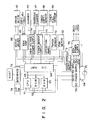
- Fig. 1 shows a structure of an EL printer.
- Photosensitive drum 42 whose surface is formed of a photoconductive material is arranged in substantially the central portion of housing 41 which is axially supported at one end, so that a portion at the other end can be vertically opened.
- Photosensitive drum 42 is rotated by drive motor 43 in one direction, i.e., in the clockwise direction in Fig. 1.
- EEH unit 45 comprises a line head including an array of a large number of EL elements, i.e., an edge emitter array head (EEH).
- EH edge emitter array head
- Transfer charger 47 is located below photosensitive drum 42. Paper sheet P is fed one by one at a predetermined timing from paper feed cassette 51 arranged at the other end side of housing 41 toward transfer charger 47 upon operation of pickup roller 52.
- paper sheet P is then exhausted onto an upper portion of the housing by exhaust rollers 54A and 54B.
- Drive motor 43 serves as a driving source of a convey mechanism for paper sheets P as well as a driving source of photosensitive drum 42.
- Fan motor 55 for dissipating internal heat outside the printer, DC power supply device 56, cover-open switch 57 for detecting a vertically opened state of housing 41, and cutting off a 24-V power supply output line from DC power supply device 56, and the like are arranged in housing 41.
- Fig. 2 is a block diagram showing a circuit arrangement.
- reference numeral 61 denotes a microprocessor (CPU) constituting a control unit main body; 62, a ROM (read-only memory) for storing program data used by CPU 61 to control respective units; 63, a RAM (random-access memory) for storing image information, and various processing data sent from an external host computer; and 64, an I/O port. These components are connected through bus line 65.
- CPU microprocessor
- 62 read-only memory
- 63 random-access memory for storing image information, and various processing data sent from an external host computer
- 64 an I/O port.
- I/O port 64 is connected to motor driver 66 for controlling drive motor 43, high voltage power supply 67 for supplying a high voltage to EEH unit 45, charger 44, and transfer charger 47, toner sensor circuit 70 for receiving signals from toner empty sensor 68 and toner full sensor 69 arranged in developer 46, operation panel 71 serving as an operation unit provided with key switches, indicators, and the like, paper sensor 72 for detecting conveyed paper sheet P, fan motor 55, interface 73 for receiving image information from the host computer, and dip switch 74.
- DC power supply 56 is connected to commercial AC power supply 75 to generate a voltage of 5 V between a 5-V terminal and an SG (ground) terminal, and to generate a voltage of 24 V between a 24-V terminal and a PG (ground) terminal.
- Cover-open switch 57 is inserted in a line connected to the 24-V terminal.
- the voltage of 5 V from DC power supply 56 is supplied to CPU 61, ROM 62, RAM 63, and I/O port 64, and the voltage of 24 V is supplied to motor driver 66, EEH unit 45, high voltage power supply 67, and fan motor 55.
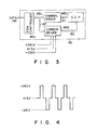
- DC power supply 56 generates voltages of 10 V, 15 V, and 27 V, and supplies them to EEH power supply 76.
- EEH power supply 76 supplies DC voltages of 260 V, 15 V, and -230 V to EEH unit 45.
- EEH unit 45 comprises EEH controller 45a for converting externally input data Din into printing data DP, channel driver 45c for applying rectangular wave voltage signal E1 having a voltage amplitude of +28 V to channel electrodes of edge emitter array head (EEH) 45b on the basis of data DP from EEH controller 45a, and common driver 45d.
- Common driver 45d receives data DP from EEH controller 45a, and DC voltages of 260 V, 15 V, and -230 V from EEH power supply 76, and applies, to common electrodes of EEH 45b, AC voltage signal pulse E2 which is periodically changed like +260 V ⁇ +15 V ⁇ -230 V ⁇ +15 V ⁇ +260 V, as shown in Fig. 4.
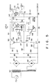
- EEH power supply 76 shown in Fig. 2 is a power supply as principal part of the present invention, and is arranged, as shown in Fig. 5. More specifically, first and second full-wave rectifies 83 and 84 are connected to AC power supply 75 via power supply transformer 82. Filter capacitors 85 and 86 are respectively connected to the DC output terminals of full-wave rectifies 83 and 84, thus constituting a voltage output circuit. Resistors 87 and 88 are connected in parallel with filter capacitors 85 and 86, respectively.
- first full-wave rectifier 83 is connected to the positive output terminal of second full-wave rectifier 84, and the node is applied with central potential Vc of 15 V from DC power supply 56 via line 89.
- the collector of NPN transistor 90 is connected to the positive output terminal of first full-wave rectifier 83, and the emitter of transistor 90 is connected to 260-V output line 91.
- NPN transistor 92 The emitter of NPN transistor 92 is connected to the negative output terminal of second full-wave rectifier 84, and the collector of transistor 92 is connected to -230-V output line 93.
- the collector and the base of transistor 90 are connected to the emitter and the collector of PNP transistor 94.
- Resistor 95 is connected between the emitter and the base of transistor 94.
- the base of transistor 94 is connected to line 89 via resistor 96, and the collector and the emitter of NPN transistor 97.
- Resistor 98 is connected between the base and the emitter of transistor 92.
- the base of transistor 92 is connected to line 89 via resistor 99 and the collector and the emitter of PNP transistor 100.
- Transistors 90, 94, and 97, and resistors 95 and 96 form a first voltage adjusting circuit
- transistors 92 and 100, and resistors 98 and 99 form a second voltage adjusting circuit.
- a voltage detector comprising a series circuit of variable resistor 101 and resistor 102, and capacitor 103 are connected between output line 91 and line 89.
- variable resistor 101 The movable terminal of variable resistor 101 is connected to the noninverting input terminal (+) of first comparator 106, and the node between resistor 104 and Zener diode 105 is connected to the inverting input terminal (-) of first comparator 106.
- a power supply circuit of first comparator 106 is connected between the 27-V power supply terminal and line 89.
- the output terminal of first comparator 106 is connected to the base of transistor 97 via resistor 107.
- a voltage divider comprising a series circuit of two resistors 108 and 109 having the same resistance is connected between output lines 91 and 93.
- Capacitor 110 is connected between line 89 and output line 93.
- Line 89 for obtaining central potential Vc is connected to the noninverting input terminal (+) of second comparator 112 via resistor 111, and the node between resistors 108 and 109 of the voltage divider is connected to the inverting input terminal (-) of second comparator 112.
- a power supply circuit of second comparator 112 is connected between the node between resistor 104 and Zener diode 105 and the 10-V power supply terminal.
- the output terminal of second comparator 112 is connected to the base of transistor 100 via resistor 113.
- Resistor 102 is connected in parallel with MOS FET (field effect transistor) 114.
- NPN transistor 116 is connected between the 27-V power supply terminal and a ground terminal via resistor 115.
- the gate of FET 114 is connected to the collector of transistor 116.
- MOS FET 114 and transistor 116 constitute a level changing means.
- Control signal S is normally a high-level signal.
- cover-open switch 57 in Fig. 1 is turned off, and control signal S becomes a low-level signal.
- an AC voltage from transformer 82 is full-wave rectified by full-wave rectifiers 83 and 84, and the rectified voltages are then filtered by filter capacitors 85 and 86, thereby generating DC voltages slightly higher than 245 V across the two terminals of capacitors 85 and 86, respectively.
- First comparator 106 compares detection potential Va input from the movable terminal of variable resistor 101 with reference potential Vref input from Zener diode 105, and controls the base current of transistor 97 so that a difference between Vref and Va becomes zero. Thus, the emitter currents of transistors 94 and 90 are controlled, and a potential difference between output line 91 and line 89 is held just at 245 V. Since a voltage of 15 V is applied from DC power supply 56 to line 89, potential Vd of output line 91 is held at a constant value of 260 V.
- potential Vd of output line 91 is determined to be 260 V in this manner, potential Ve of output line 93 is automatically determined to be -230 V. Therefore, potentials of 260 V and -230 V can be easily obtained by only adjusting variable resistor 101. More specifically, an adjusting operation can be facilitated.
- central potential Vc 15 V is determined as a fundamental voltage for generating a reference voltage to be input to first and second comparators 106 and 112, when the central potential is changed, potentials Vd and Ve of output lines 91 and 93 can be changed in the same manner as the central potential. Therefore, positive and negative potentials Vd and Ve can be simultaneously changed.
- EEH unit 45 In this manner, voltages of 260 V, 15 V, and -230 V are supplied from EEH power supply 76 to common driver 45d of EEH unit 45.
- Common driver 45d supplies an AC voltage signal pulse which is periodically changed like +260 V ⁇ +15 V ⁇ -230 V ⁇ +15 V ⁇ +260 V, to the common electrodes of the EL elements of EEH 45b. In this manner, EEH unit 45 is ready to perform an exposure operation.
- the photosensitive body of photosensitive drum 42 is uniformly changed by charger 44, and is then exposed by a light-emitting operation of EEH 45b of EEH unit 45, so that image information is recorded thereon as an electrostatic latent image.
- the electrostatic latent image is developed with a toner by developer 46, and the toner image is transferred by transfer charger 47 onto a paper sheet fed from paper feed cassette 51. Thereafter, the paper sheet is exhausted through fixing device 53 and exhaust rollers 54A and 54B. Any residual toner is removed by cleaning device 49 from the photosensitive body after the transfer operation.
- the photosensitive body is then discharged by discharging device 50 to prepare for the next charging operation.
- control signal S to be supplied from I/O port 64 to EEH power supply 76 goes to low level.
- transistor 116 is disabled, and FET 114 is enabled.
- the level of detection potential Va input from variable resistor 101 to first comparator 106 is decreased to be lower than the level of reference potential Vref input from Zener diode 105.
- the output level from first comparator 106 becomes low level, so that transistor 97 is disabled, and transistors 90 and 94 are disabled. Then, positive voltage output line 91 is disconnected from the positive terminal of filter capacitor 85.
- Fig. 6 shows a modification of EEH power supply 76 shown in Fig. 5.
- Figs. 5 and 6 illustrate substantially the same circuit arrangements of the power supply regulators except for an arrangement for stopping voltage outputs.
- transistor 116 is enabled, and transistor 114 is disabled in response to high-level signal S, and detection potential Va is increased to satisfy Va > Vref, thereby decreasing voltages +Vd and -Ve.
- transistor 116 is enabled in response to high-level signal S, and reference potential Vref is decreased to be lower than Vc + Vz and to satisfy Va > Vref, thereby decreasing voltages +Vd and -Ve.
- resistances R108 and R109 of resistors 108 and 109 are set to be equal to each other.
- , but if R108 nR109,
- n
- the present invention is applied to a power supply for driving a common driver of a line head having an array of EL elements, which is used as an exposure device in an EL printer.
- the present invention is not limited to this.
- a power supply device which can easily stop positive and negative relatively high voltage outputs under the external control, and has a simple circuit arrangement for attaining the control can be provided.
Landscapes
- Physics & Mathematics (AREA)
- Engineering & Computer Science (AREA)
- General Physics & Mathematics (AREA)
- Optics & Photonics (AREA)
- General Engineering & Computer Science (AREA)
- Theoretical Computer Science (AREA)
- Electromagnetism (AREA)
- Radar, Positioning & Navigation (AREA)
- Automation & Control Theory (AREA)
- Control Or Security For Electrophotography (AREA)
Applications Claiming Priority (4)
| Application Number | Priority Date | Filing Date | Title |
|---|---|---|---|
| JP7283090A JP2796400B2 (ja) | 1990-03-22 | 1990-03-22 | 電源装置 |
| JP72830/90 | 1990-03-22 | ||
| JP7282890A JP2796399B2 (ja) | 1990-03-22 | 1990-03-22 | 電源装置 |
| JP72828/90 | 1990-03-22 |
Publications (3)
| Publication Number | Publication Date |
|---|---|
| EP0448026A2 true EP0448026A2 (fr) | 1991-09-25 |
| EP0448026A3 EP0448026A3 (en) | 1992-11-19 |
| EP0448026B1 EP0448026B1 (fr) | 1994-11-30 |
Family
ID=26413964
Family Applications (1)
| Application Number | Title | Priority Date | Filing Date |
|---|---|---|---|
| EP91104189A Expired - Lifetime EP0448026B1 (fr) | 1990-03-22 | 1991-03-18 | Alimentation en courant électrique. |
Country Status (4)
| Country | Link |
|---|---|
| US (1) | US5144364A (fr) |
| EP (1) | EP0448026B1 (fr) |
| KR (1) | KR940002426B1 (fr) |
| DE (1) | DE69105318T2 (fr) |
Cited By (2)
| Publication number | Priority date | Publication date | Assignee | Title |
|---|---|---|---|---|
| EP0712207A3 (fr) * | 1994-11-14 | 1996-09-25 | Hewlett Packard Co | Alimentation de puissance pur une puissance résiduelle temporisée après le blocage |
| EP0860754A3 (fr) * | 1997-02-21 | 1999-05-19 | Sharp Kabushiki Kaisha | Appareil de formation d'images |
Families Citing this family (3)
| Publication number | Priority date | Publication date | Assignee | Title |
|---|---|---|---|---|
| JP2783946B2 (ja) * | 1992-08-20 | 1998-08-06 | 株式会社テック | 端面発光型ラインヘッドの駆動装置 |
| US8692165B2 (en) * | 2003-01-06 | 2014-04-08 | Bunn-O-Matic Corporation | Power circuitry incorporating both foreign and domestic alternating current line voltages for a heated beverage apparatus |
| US9643439B2 (en) | 2013-09-20 | 2017-05-09 | Veltek Associates, Inc. | Portable cleanroom printing cabinet |
Family Cites Families (7)
| Publication number | Priority date | Publication date | Assignee | Title |
|---|---|---|---|---|
| US3504272A (en) * | 1968-05-31 | 1970-03-31 | Hewlett Packard Co | Power supply having interconnected voltage regulators providing multiple outputs |
| US4239373A (en) * | 1978-11-01 | 1980-12-16 | Xerox Corporation | Full wave rectification apparatus for operation of DC corotrons |
| US4234249A (en) * | 1978-11-01 | 1980-11-18 | Xerox Corporation | Tracking power supply for AC and DC corotrons |
| US4320447A (en) * | 1980-11-12 | 1982-03-16 | Krauss Geoffrey H | Fail-safe amplifier power supply |
| DE3139066A1 (de) * | 1981-10-01 | 1983-04-14 | Johnson Service Co., Milwaukee, Wis. | Netzgeraet |
| DE3303450A1 (de) * | 1982-02-04 | 1983-08-11 | Canon K.K., Tokyo | Steuereinrichtung fuer kopiergeraete oder dergleichen |
| US4535341A (en) * | 1983-08-19 | 1985-08-13 | Westinghouse Electric Corp. | Thin film electroluminescent line array emitter and printer |
-
1991
- 1991-03-14 US US07/669,384 patent/US5144364A/en not_active Expired - Fee Related
- 1991-03-18 DE DE69105318T patent/DE69105318T2/de not_active Expired - Fee Related
- 1991-03-18 EP EP91104189A patent/EP0448026B1/fr not_active Expired - Lifetime
- 1991-03-20 KR KR1019910004409A patent/KR940002426B1/ko not_active Expired - Fee Related
Cited By (3)
| Publication number | Priority date | Publication date | Assignee | Title |
|---|---|---|---|---|
| EP0712207A3 (fr) * | 1994-11-14 | 1996-09-25 | Hewlett Packard Co | Alimentation de puissance pur une puissance résiduelle temporisée après le blocage |
| EP0860754A3 (fr) * | 1997-02-21 | 1999-05-19 | Sharp Kabushiki Kaisha | Appareil de formation d'images |
| US6003976A (en) * | 1997-02-21 | 1999-12-21 | Sharp Kabushiki Kaisha | Apparatus for electrostatically forming images using time stable reference voltage |
Also Published As
| Publication number | Publication date |
|---|---|
| KR940002426B1 (ko) | 1994-03-24 |
| KR910017249A (ko) | 1991-11-05 |
| EP0448026A3 (en) | 1992-11-19 |
| DE69105318T2 (de) | 1995-04-06 |
| US5144364A (en) | 1992-09-01 |
| EP0448026B1 (fr) | 1994-11-30 |
| DE69105318D1 (de) | 1995-01-12 |
Similar Documents
| Publication | Publication Date | Title |
|---|---|---|
| US8019241B2 (en) | Image forming apparatus | |
| US5099287A (en) | Transferring voltage control section | |
| US5191362A (en) | Electrophotographic printing apparatus with a control system responsive to temperature changes | |
| US4583836A (en) | Abnormal condition detection device for corona discharger in electrophotographic copying machine | |
| US6070025A (en) | Technique for controlling transfer voltage in an image forming apparatus in accordance with detected composite resistance between photoconductive drum and transfer roller | |
| EP0448026B1 (fr) | Alimentation en courant électrique. | |
| US5237339A (en) | Electrophotography apparatus | |
| US6731892B2 (en) | Image forming apparatus having high-voltage power supply | |
| JPH01142739A (ja) | 現像器脱着型記録装置 | |
| JP2728831B2 (ja) | 3レベル像形成装置の作動中に電荷保持表面上に3レベル像を形成する方法及び装置 | |
| JPH07160098A (ja) | 画像形成装置 | |
| JP2796399B2 (ja) | 電源装置 | |
| JP2796400B2 (ja) | 電源装置 | |
| JP2733362B2 (ja) | 電子写真装置 | |
| JP2690403B2 (ja) | 電子写真プリント装置 | |
| JP3437699B2 (ja) | 帯電装置 | |
| JP3354919B2 (ja) | 画像形成装置 | |
| JPH0739352Y2 (ja) | 複写機用高圧電源装置 | |
| JPH05150613A (ja) | コロナ放電装置 | |
| JP3414006B2 (ja) | 転写装置 | |
| JP3782570B2 (ja) | 画像記録装置 | |
| JP2611988B2 (ja) | 放電装置 | |
| JPH0540397A (ja) | コロトロン用高圧電源出力の自動調整方法 | |
| JPH06230656A (ja) | コロナ放電装置 | |
| JPS6159460A (ja) | 帯電用高圧電源 |
Legal Events
| Date | Code | Title | Description |
|---|---|---|---|
| PUAI | Public reference made under article 153(3) epc to a published international application that has entered the european phase |
Free format text: ORIGINAL CODE: 0009012 |
|
| 17P | Request for examination filed |
Effective date: 19910318 |
|
| AK | Designated contracting states |
Kind code of ref document: A2 Designated state(s): DE FR GB IT NL |
|
| PUAL | Search report despatched |
Free format text: ORIGINAL CODE: 0009013 |
|
| AK | Designated contracting states |
Kind code of ref document: A3 Designated state(s): DE FR GB IT NL |
|
| 17Q | First examination report despatched |
Effective date: 19930622 |
|
| GRAA | (expected) grant |
Free format text: ORIGINAL CODE: 0009210 |
|
| AK | Designated contracting states |
Kind code of ref document: B1 Designated state(s): DE FR GB IT NL |
|
| PG25 | Lapsed in a contracting state [announced via postgrant information from national office to epo] |
Ref country code: IT Free format text: LAPSE BECAUSE OF FAILURE TO SUBMIT A TRANSLATION OF THE DESCRIPTION OR TO PAY THE FEE WITHIN THE PRE;WARNING: LAPSES OF ITALIAN PATENTS WITH EFFECTIVE DATE BEFORE 2007 MAY HAVE OCCURRED AT ANY TIME BEFORE 2007. THE CORRECT EFFECTIVE DATE MAY BE DIFFERENT FROM THE ONE RECORDED.SCRIBED TIME-LIMIT Effective date: 19941130 Ref country code: NL Effective date: 19941130 Ref country code: FR Effective date: 19941130 |
|
| REF | Corresponds to: |
Ref document number: 69105318 Country of ref document: DE Date of ref document: 19950112 |
|
| EN | Fr: translation not filed | ||
| NLV1 | Nl: lapsed or annulled due to failure to fulfill the requirements of art. 29p and 29m of the patents act | ||
| PLBE | No opposition filed within time limit |
Free format text: ORIGINAL CODE: 0009261 |
|
| STAA | Information on the status of an ep patent application or granted ep patent |
Free format text: STATUS: NO OPPOSITION FILED WITHIN TIME LIMIT |
|
| 26N | No opposition filed | ||
| PGFP | Annual fee paid to national office [announced via postgrant information from national office to epo] |
Ref country code: GB Payment date: 19960311 Year of fee payment: 6 |
|
| PGFP | Annual fee paid to national office [announced via postgrant information from national office to epo] |
Ref country code: DE Payment date: 19960328 Year of fee payment: 6 |
|
| PG25 | Lapsed in a contracting state [announced via postgrant information from national office to epo] |
Ref country code: GB Effective date: 19970318 |
|
| GBPC | Gb: european patent ceased through non-payment of renewal fee |
Effective date: 19970318 |
|
| PG25 | Lapsed in a contracting state [announced via postgrant information from national office to epo] |
Ref country code: DE Effective date: 19971202 |