EP0448024A2 - Appareil de géneration d'image comprenant un circuit de traitement d'inclinaison - Google Patents
Appareil de géneration d'image comprenant un circuit de traitement d'inclinaison Download PDFInfo
- Publication number
- EP0448024A2 EP0448024A2 EP91104182A EP91104182A EP0448024A2 EP 0448024 A2 EP0448024 A2 EP 0448024A2 EP 91104182 A EP91104182 A EP 91104182A EP 91104182 A EP91104182 A EP 91104182A EP 0448024 A2 EP0448024 A2 EP 0448024A2
- Authority
- EP
- European Patent Office
- Prior art keywords
- skew
- image data
- count means
- count
- processing
- Prior art date
- Legal status (The legal status is an assumption and is not a legal conclusion. Google has not performed a legal analysis and makes no representation as to the accuracy of the status listed.)
- Granted
Links
Images


Classifications
-
- G—PHYSICS
- G06—COMPUTING OR CALCULATING; COUNTING
- G06T—IMAGE DATA PROCESSING OR GENERATION, IN GENERAL
- G06T3/00—Geometric image transformations in the plane of the image
- G06T3/60—Rotation of whole images or parts thereof
- G06T3/608—Rotation of whole images or parts thereof by skew deformation, e.g. two-pass or three-pass rotation
-
- H—ELECTRICITY
- H04—ELECTRIC COMMUNICATION TECHNIQUE
- H04N—PICTORIAL COMMUNICATION, e.g. TELEVISION
- H04N1/00—Scanning, transmission or reproduction of documents or the like, e.g. facsimile transmission; Details thereof
- H04N1/387—Composing, repositioning or otherwise geometrically modifying originals
- H04N1/3877—Image rotation
- H04N1/3878—Skew detection or correction
Definitions
- the present invention relates to a skew processing circuit for a digital image formation device.
- a skew processing in a conventional digital copying machine is performed to the whole image of an original sheet read out. More specifically, the whole original image rectangular in shape is processed into the skew to make a parallelogram image.
- a general object of the present invention to provide a skew processing circuit capable of performing a partial skew processing to an original image which a conventional skew processing circuit cannot accomplish.
- a provided original image is selectively processed into the skew, and simply a desired area of the image data can be transformed into skew image data.
- an area void of data is produced as a result of a skew processing of an image data by a skew processing means; the data void area is masked so that an original image identical with a skew image might not be outputted in the data void area.
- the resultant output is skew image data existing in original image data in a good condition.
- an area to be processed into the skew is specified, when, as a result of a skew processing of image data in that area, the image data is slanted at the head or the tail of the area partially out to the exterior of the specified area, either of an original image data or a skew image data in that part can take precedence over each other.
- specifying an initial point of a skew image makes it possible to arbitrarily set an effective area of the skew processing.
- an amount of shifting a processing address is determined by a base counting means, a base clear counting means and a combination counting means; therefore, image data is shifted by the optimum address shift amount depending upon a preset angle, and a good skew image can be obtained in a wide range of an angle.
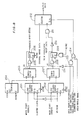
- Fig. 1 is a block diagram showing an overall system architecture of a digital copying machine having a skew processing circuit of an embodiment according to the present invention.
- An original image (not shown) is read by an image scan unit 1; original image data read out is converted by an A/D converter 2 into digital data, and it is applied to an image processing circuit 3.
- the image processing circuit 3 includes a shading compensating circuit 31, a logarithmic compensating circuit 32 and a skew processing circuit 33 characterizing the this embodiment.
- Image data processed by the image processing circuit 3 is applied to a pattern generator 4; an output of the pattern generator 4 causes a laser scan unit 5 to operate, and an image is reproduced.
- the image processing circuit 3 is placed under the control of a CPU 6 which controls the whole digital copying machine. Connected to the CPU 6 are a ROM 7 having its operation program stored and a RAM 8 serving as a storing device in and from which data is freely written and read out.
- an area specifying device such as a tablet 9 and the like.
- the tablet 9 is utilized to make an input specification on an area to be processed into the skew, an angle of the skew (an inclination angle of an image) and a direction of the skew (whether the image is slanted to the left (the positive direction) or to the right (the negative direction)); simply an image data of the area specified by an input is processed into the skew by the skew processing circuit 33 at a specified angle in a specified direction.
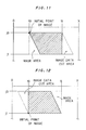
- Fig. 2A, 2B and 2C are diagrams for explaining procedures of the skew processing in this embodiment.
- the skew processing means a data processing in which a rectangular area a with hatching in an original image shown in Fig. 2A is slanted, for example, to the left (in the positive direction) at a desired angle &H to obtain a copy containing a skew image as shown in Fig. 2B; otherwise, it means a data processing in which the rectangular area a with hatching in the original image shown in Fig. 2A is slanted, for example, to the right (in the negative direction) at a desired angle &H to obtain a copy containing a skew image as shown in Fig. 2C.
- an area 1 with hatching has the skew image and the original image overlapping with each other; so in this embodiment, giving precedence to the original image, the processing is executed without outputting the skew image.
- an area 2 a skew image identical with the original image appearing in an area 3 appears; therefore, an output is masked so that a blank image (or a solid image) appears.
- a copy having an area 4 with check slanted in the positive direction into the skew image is obtained.
- Fig. 3 is a block diagram for explaining the skew processing circuit in this embodiment.
- the skew processing circuit 33 in this embodiment two line buffers, a skew processing type line buffer 331 and an original type line buffer 332, and a write/read control circuit 333 for controlling the two line buffers.
- the write/read control circuit 333 is a control circuit which writes a given image data in single lines in the two line buffers 331, 332 and selectively reads data written in the two line buffers 331, 332. When image data is written in the original type line buffer 332, it is sequentially written from the head address 0.
- a write start address RH0 is determined in correspondence with a skew angle; the write start address RH0 is shifted in each line, and the head portion of the image data is discarded by specified dots (by a specified address).
- RH0 (j1 - j0) x tan ⁇
- the write start address RH0 is, as explained later, sequentially shifted in accordance with a preset value of a counter which is determined in correspondence with the skew angle ⁇ .
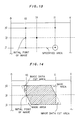
- the write/read control circuit 333 reads an image data from the skew processing type line buffer 331 for the specified area processed into the skew (the rectangular area having apexes (i0, j0) (i1, j0) (i0, j1) (i1, j1)) but reads an image data from the original type line buffer 332 for the remaining area.
- the reading out of the image data will be explained in detail later.
- Fig. 4 is a diagram showing an example of shifting the write start address RH0 in the case of writing an image data in the skew processing type line buffer 331.
- the data is written without shifting the write start address RH0 in the first and second lines; the data is written with the write start address RH0 shifted by a single dot (with the head of the image data discarded by another single dot) in the third and fourth lines; the data is written with the write start address RH0 shifted by two dots in the fifth and sixth lines; the data is written with the write start address RH0 shifted by three dots in the seventh, eighth and ninth lines; in the tenth line and after, the data is written with the write start address RH0 sequentially shifted by repetition of the operation beginning with the first line.
- Tables 1 and 2 below show counter preset values for shifting the write start address RH0 for the skew processing, respective values for each skew angle.
- Figs. 5A and 5B are flow charts for calculating the preset values of the counters shown in Table 1.
- the skew angle ⁇ is set from 1° through 45° in the count setting table (Table 1) (Step S1). Then, an initialization is carried out to clear the base count n, the clear count x, the combination count m and a tolerance count (a count value of a register for keeping the figure of the first decimal place as a result of the operation) (Step S2). Then, the preset maximum value i of the base count n, the preset maximum value j of the combination count m, and the preset maximum value k of the clear count x are specified (Step S3).
- Step S11 the value of the first decimal place (0 in this case) of the calculated skew angle ⁇ is defined as DP1 (Step S11), and it is judged whether DP1 is equal to or over 5 (Step S12).
- the calculated skew angle ⁇ is rounded to the nearest whole number by counting 0.5 and over as a unit regarding to the value (DP1) in the first decimal place (Step S15).
- Step S18 the preset value of the clear count x is incremented by "1" (Step S18), and the procedure of Step 9 and after is repeated.
- and def2
- Step S21 def1 > def2 is satisfied, it is judged whether def 1 ⁇ 1 (Step S24); if the answer is NO, it is further judged whether ks ⁇ Se (Step S25).
- Step S18 clear count X is further incremented by "1" .
- the processing routine at Steps S19 through S25 is a compensation processing routine which, in the case where x, n, m and Se corresponding to the skew angle ⁇ have been found, preferentially chooses ones of the variables that has a difference between n and m as small as possible and sets them as count values.
- the skew angle ⁇ is calculated from 45° , 44° , 43° , 42° , ..., up to 1° , and the count values corresponding to them are found.
- the obtained results of the operation are shown in Tables 1 and 2, as have been stated.
- Fig. 6 shows a circuit included by the write/read control circuit 333 (see Fig. 3), for producing a skew processing type address shift clock based upon the base counter preset value n, the clear counter preset value x and the combination counter preset value m shown in Tables 1 and 2.
- Figs. 7A and 7B are timing charts showing the operation of the circuit in Fig. 6.
- the address shift clock producing circuit can be divided into three sections: a base count type circuit in the upper stage, a combination count type circuit in the middle stage, and a clear count type circuit in the bottom stage.
- a horizontal synchronization signal (HSYNC) is counted by a base counter 101.
- a count value of the base counter 101 is applied to a comparator 102 and compared with the preset value n for the base counter (the preset value n is loaded in the comparator based upon Tables 1 and 2).
- the count value of the base counter 101 is identical with the preset value n, an EQ output of the comparator 102 turns high and is applied to a D flip flop 103.
- the D flip flop 103 receives a clock under the condition that the EQ signal of high is being applied, an output of the D flip flop turns high.
- the next output of a D flip flop 104 is low; as it is inverted by an inverter 105 to turn high, a slanting clock is outputted through an AND gate 106 and an OR gate 107. Then, when the next clock is applied to the D flip flop 104, an output of the D flip flop turns high, the slanting clock turns low; an output of a NAND gate 110 turns low because of a high output which is a high output of the D flip flop 104 and a low output of a D flip flop 108 inverted by an inverter 109; a clear pulse is applied through an AND gate 111 to the base counter 101, and thus the base counter is cleared.
- the slanting clock outputted by the AND gate 106 is applied to a clear counter 112 and counted.
- a count value of the clear counter 112 is compared with the clear counter preset value x (the preset value is also loaded based upon Table 1) by a comparator 113.
- an EQ output is drawn from the comparator 113 and applied through the OR gate 114 to a D flip flop 115.
- the D flip flop 115 under the condition that the EQ output of high is being applied has an output turned high when the horizontal synchronization signal turns low. Since the high output is returned through the OR gate to the D flip flop 115, the D flip flop is in self- holding.
- the high output of the D flip flop 115 is inverted to low by an inverter 116 and clears the base counter 101 through the AND gate 111.
- a slanting clock is drawn by the base count circuit in the upper stage every preset value n of the base counter, and this is repeated until it reaches the preset value x of the clear counter by the clear count circuit in the bottom stage.
- a count signal is applied through an AND gate 117 to a combination counter 118.
- the combination counter 118 counts the number of the applied horizontal synchronization signals and applies it to a comparator 119. From the comparator 119, an EQ output of high is drawn when a count value of the horizontal synchronization signal is identical with the preset value m set in advance (the preset value is also loaded based upon Tables 1 and 2). Then, the high EQ output is applied to a D flip flop 120.
- An output of the D flip flop 120 turns high in response to a clock input; since a low output of a D flip flop is inverted by an inverter 122, a slanting clock is outputted from an AND gate 123. Then, when the next clock is applied, an output of the D flip flop turns high; as an output of a D flip flop 124 is low, it is inverted to high by an inverter 125, a clear pulse is outputted from an NAND gate 126, and the whole circuit is cleared to the initial state.
- Fig. 8 is a circuit diagram of the skew processing type address control signal producing circuit. The circuit is included by the write/read control circuit 333 (see Fig. 3).
- the circuit controls the write start address RH0 of the image data to the skew processing line buffer 331 (see Fig. 3) based upon the write start address previously explained and also shifts the write start address RH0 in accordance with a produced slanting clock. Furthermore, it masks the reading of the image data from the skew processing line buffer 331 by the mask start address MH0 previously explained and also shifts the mask master address MH0 by the slanting clock. Moreover, the circuit controls the selective reading of data from the original type line buffer 332 and the skew processing type line buffer 331.
- Fig. 9 is a timing chart of the circuit of Fig. 8. Now, with reference to Fig. 9, the circuit of Fig. 8 will be specifically explained.
- a write type up-down counter 201 the write start address RH0 is loaded. Also in a mask type up-down counter 202, the mask start address MH0 is loaded.
- up count or down count of the up-down counters 201, 202 are specified. More specifically, the write type up-down counter 201 is set for down count while the mask type up-down counter is set for up count when the skew angle is in the positive direction. In the case where the skew angle is in the negative direction, the write type up-down counter 201 is set for up count, while the mask type up-down counter 202 is set for down count.
- the write type up-down counter 201 receiving a slanting clock, executes an up count or down count from an initial value of the loaded write start address RH0. Then, the count value is applied to a comparator 203. In the comparator 203, the number of counted dots applied by the dot counter 204 is compared with a count number of the up-down counter 201 for every single line.
- the slanting clock is a clock outputted each time the write start address RH0 has to be shifted; so receiving the slanting block, the count value of the up-down counter 201, or the write start address RH0, is shifted, and it is compared with a count value of the dot counter 204 by the comparator 203.
- the D flip flop 206 Since an area enable signal in the secondary scanning direction is inverted by an inverter 215 and applied to the OR gate 205, the D flip flop 206 always outputs a high address reset signal with regard to the outside of the area to be processed into the skew in the secondary scanning direction; therefore, the writing of the image data is never limited.
- the mask start address MH0 loaded in the mask type up-down counter 202 is counted up or down by the slanting clock, and the count value is applied to the comparator 207.
- a count value of the dot counter 204 is compared with a count value of the up-down counter 202; when both the count values come to be identical with each other, that is, when the count value of the dot counter 204 which is an address of an image reaches the count value of the up-down counter 202 for every single line, an EQ output of high is drawn.
- the output is applied through the OR gate 208 to the D flip flop 209. Then, in response to a clock input, an output of the D flip flop 209 is self-held.
- the D flip flop 209 is cleared by a horizontal synchronization signal and outputs a mask start signal for each single line.
- a selector 212 Based upon the area enable signal (in the secondary and primary directions) or an area specification/the whole image specification switching signal, a selector 212 is switched. More specifically, when both the area enable signals in the secondary and primary directions are high, a high signal is applied through an AND gate 213 and an OR gate 214 to a switching terminal of the selector 212. Thus, the selector 212 selects the skew processed image data applied to a B terminal as an output data.
- the area enable signal in the secondary scanning direction or the area enable signal in the primary scanning direction is low, that is, when the outside of the skew processed area specified by the tablet 9 (see Fig. 1) is selected, a low signal is applied as a switching signal to the selector 212; hence, the original image data applied to the A terminal is selected as an output data.
- Fig. 10 is a circuit diagram showing a skew processing type address control circuit of another embodiment.
- the circuit is different from the circuit shown in Fig. 8 in that the skew processed image is preferentially outputted when the skew processed image overlaps with the original image. Therefore, this circuit is composed of the circuit shown in Fig. 8 and a skew image type up-down counter 231, a comparator 232, an OR gate 233 and a D flip flop 234 connected thereto.
- An operation timing of the circuit is shown in Fig. 9.
- a skew image output address is loaded into the skew image type up-down counter 231.
- the skew image output address is i0 - (j1 - j0) tan ⁇ .
- the skew image type up-down counter 231 is set so that it takes an up count when the skew angle is in the positive direction and takes a down count when it is in the negative direction.
- a count value of the dot counter 204 is compared with a count value of the skew image type up-down counter 231; when the count value of the dot counter 204 is identical with the count value of the skew image type up-down counter 231, an EQ output of high is drawn, and the output is applied through the OR gate 233 to the D flip flop 234.
- the D flip flop 234 is self-held in response to a clock input, while its high output is applied through an AND gate and an OR gate to the selector 212 as a select signal, and skew processing image data is selected.
- the AND gate 213 turns to the low level, and the selector 212 selectively outputs an original image data.
- the cut area and mask area of the skew processed image are changed.
- an initial point of the image is also set (the setting can be performed by specifying an arbitrary point in the skew processed area on a tablet), so that an effective area of the skew processed image is attained as a desired one, and the desired area can be processed into the skew.
- the area to be processed into the skew is specified.
- two points like (i0, j0) (i1, j1) or (i1, j0) (i0, j1) are specified, and the area to be processed into the skew is specified.
- the skew processed image can be attained as a desired image.
- the embodiments in which an arbitrary area in an original image can be copied as a skew processed image are discussed; however, the arbitrary area for the skew processed image may be more than a single area.
- the arbitrary area for the skew processed image may be more than a single area.
- a plurality of different areas can be specified in the secondary scanning direction as areas to be processed into the skew.
- the skew angle and skew direction is changed for each of the specified areas, and the contents processed into the skew are individually set.
Landscapes
- Engineering & Computer Science (AREA)
- Physics & Mathematics (AREA)
- General Physics & Mathematics (AREA)
- Theoretical Computer Science (AREA)
- Multimedia (AREA)
- Signal Processing (AREA)
- Editing Of Facsimile Originals (AREA)
Applications Claiming Priority (4)
| Application Number | Priority Date | Filing Date | Title |
|---|---|---|---|
| JP70300/90 | 1990-03-20 | ||
| JP2070300A JP2596628B2 (ja) | 1990-03-20 | 1990-03-20 | 斜体処理回路 |
| JP2070299A JP2548817B2 (ja) | 1990-03-20 | 1990-03-20 | 斜体処理回路 |
| JP70299/90 | 1990-03-20 |
Publications (3)
| Publication Number | Publication Date |
|---|---|
| EP0448024A2 true EP0448024A2 (fr) | 1991-09-25 |
| EP0448024A3 EP0448024A3 (en) | 1992-03-25 |
| EP0448024B1 EP0448024B1 (fr) | 1996-06-12 |
Family
ID=26411465
Family Applications (1)
| Application Number | Title | Priority Date | Filing Date |
|---|---|---|---|
| EP91104182A Expired - Lifetime EP0448024B1 (fr) | 1990-03-20 | 1991-03-18 | Appareil de géneration d'image comprenant un circuit de traitement d'inclinaison |
Country Status (3)
| Country | Link |
|---|---|
| US (1) | US5418896A (fr) |
| EP (1) | EP0448024B1 (fr) |
| DE (1) | DE69120119T2 (fr) |
Families Citing this family (3)
| Publication number | Priority date | Publication date | Assignee | Title |
|---|---|---|---|---|
| US5742297A (en) * | 1994-11-04 | 1998-04-21 | Lockheed Martin Corporation | Apparatus and method for constructing a mosaic of data |
| US6636649B1 (en) * | 1998-10-16 | 2003-10-21 | Matsushita Electric Industrial Co., Ltd. | Image processing apparatus and the method of correcting the inclination |
| JP5899918B2 (ja) * | 2011-12-27 | 2016-04-06 | 株式会社リコー | 画像処理装置、画像処理方法 |
Family Cites Families (3)
| Publication number | Priority date | Publication date | Assignee | Title |
|---|---|---|---|---|
| JPS59163947A (ja) * | 1983-03-08 | 1984-09-17 | Dainippon Screen Mfg Co Ltd | 画像変形方法 |
| US4788599A (en) * | 1986-04-01 | 1988-11-29 | Canon Kabushiki Kaisha | Image processing with image-slant control and/or image-size control |
| US5187753A (en) * | 1989-12-08 | 1993-02-16 | Xerox Corporation | Method and apparatus for identification and correction of document skew |
-
1991
- 1991-03-14 US US07/669,628 patent/US5418896A/en not_active Expired - Fee Related
- 1991-03-18 EP EP91104182A patent/EP0448024B1/fr not_active Expired - Lifetime
- 1991-03-18 DE DE69120119T patent/DE69120119T2/de not_active Expired - Fee Related
Also Published As
| Publication number | Publication date |
|---|---|
| DE69120119D1 (de) | 1996-07-18 |
| DE69120119T2 (de) | 1997-02-06 |
| EP0448024B1 (fr) | 1996-06-12 |
| EP0448024A3 (en) | 1992-03-25 |
| US5418896A (en) | 1995-05-23 |
Similar Documents
| Publication | Publication Date | Title |
|---|---|---|
| US5086346A (en) | Image processing apparatus having area designation function | |
| US4694342A (en) | Spatial filter useful for removing noise from video images and for preserving detail therein | |
| EP0006351A1 (fr) | Méthode de traitement de données d'image | |
| EP0238976B1 (fr) | Procédé et appareil pour la génération de teintes | |
| US4503469A (en) | Picture image enlarging/reducing system | |
| US4533942A (en) | Method and apparatus for reproducing an image which has a coarser resolution than utilized in scanning of the image | |
| US4905079A (en) | Color image processing apparatus for processing separated color signals | |
| EP0448024A2 (fr) | Appareil de géneration d'image comprenant un circuit de traitement d'inclinaison | |
| US4591905A (en) | Color image data processing device for correcting red ghosts of black images | |
| US5289270A (en) | Image processing apparatus for performing density conversion | |
| US5257120A (en) | Image processing apparatus | |
| EP0452933B1 (fr) | Procédé et appareil pour la lecture d'images | |
| JP2794260B2 (ja) | デジタル画像処理システムの領域信号生成方法及び装置 | |
| US4860117A (en) | Image processing method and system using multiple image sensors producing image data segments which are combined and subjected to optical processing | |
| JPH06152929A (ja) | 画像形成装置 | |
| EP0673148A2 (fr) | Appareil de traitement d'images à agrandissement variable | |
| JPH02295351A (ja) | 画像処理システム | |
| JP2918906B2 (ja) | 画像処理方法及びその装置 | |
| JPS634749B2 (fr) | ||
| JP2756278B2 (ja) | 画像処理装置 | |
| JP2548817B2 (ja) | 斜体処理回路 | |
| JP2921850B2 (ja) | 画像処理装置 | |
| JPH0396070A (ja) | 画像変倍装置 | |
| JPH03270472A (ja) | 斜体処理回路 | |
| JP3123133B2 (ja) | 画像編集装置 |
Legal Events
| Date | Code | Title | Description |
|---|---|---|---|
| PUAI | Public reference made under article 153(3) epc to a published international application that has entered the european phase |
Free format text: ORIGINAL CODE: 0009012 |
|
| AK | Designated contracting states |
Kind code of ref document: A2 Designated state(s): DE FR GB IT |
|
| PUAL | Search report despatched |
Free format text: ORIGINAL CODE: 0009013 |
|
| AK | Designated contracting states |
Kind code of ref document: A3 Designated state(s): DE FR GB IT |
|
| 17P | Request for examination filed |
Effective date: 19920529 |
|
| 17Q | First examination report despatched |
Effective date: 19940714 |
|
| GRAH | Despatch of communication of intention to grant a patent |
Free format text: ORIGINAL CODE: EPIDOS IGRA |
|
| GRAA | (expected) grant |
Free format text: ORIGINAL CODE: 0009210 |
|
| AK | Designated contracting states |
Kind code of ref document: B1 Designated state(s): DE FR GB IT |
|
| REF | Corresponds to: |
Ref document number: 69120119 Country of ref document: DE Date of ref document: 19960718 |
|
| ET | Fr: translation filed | ||
| ITF | It: translation for a ep patent filed | ||
| PG25 | Lapsed in a contracting state [announced via postgrant information from national office to epo] |
Ref country code: GB Effective date: 19970318 |
|
| PLBE | No opposition filed within time limit |
Free format text: ORIGINAL CODE: 0009261 |
|
| STAA | Information on the status of an ep patent application or granted ep patent |
Free format text: STATUS: NO OPPOSITION FILED WITHIN TIME LIMIT |
|
| 26N | No opposition filed | ||
| GBPC | Gb: european patent ceased through non-payment of renewal fee |
Effective date: 19970318 |
|
| PG25 | Lapsed in a contracting state [announced via postgrant information from national office to epo] |
Ref country code: FR Free format text: LAPSE BECAUSE OF NON-PAYMENT OF DUE FEES Effective date: 19971128 |
|
| PG25 | Lapsed in a contracting state [announced via postgrant information from national office to epo] |
Ref country code: DE Effective date: 19971202 |
|
| REG | Reference to a national code |
Ref country code: FR Ref legal event code: ST |
|
| PG25 | Lapsed in a contracting state [announced via postgrant information from national office to epo] |
Ref country code: IT Free format text: LAPSE BECAUSE OF NON-PAYMENT OF DUE FEES;WARNING: LAPSES OF ITALIAN PATENTS WITH EFFECTIVE DATE BEFORE 2007 MAY HAVE OCCURRED AT ANY TIME BEFORE 2007. THE CORRECT EFFECTIVE DATE MAY BE DIFFERENT FROM THE ONE RECORDED. Effective date: 20050318 |