EP0446571A2 - Circuit PLL à boucle unique - Google Patents
Circuit PLL à boucle unique Download PDFInfo
- Publication number
- EP0446571A2 EP0446571A2 EP19910100299 EP91100299A EP0446571A2 EP 0446571 A2 EP0446571 A2 EP 0446571A2 EP 19910100299 EP19910100299 EP 19910100299 EP 91100299 A EP91100299 A EP 91100299A EP 0446571 A2 EP0446571 A2 EP 0446571A2
- Authority
- EP
- European Patent Office
- Prior art keywords
- pll circuit
- output
- voltage
- vco
- loop
- Prior art date
- Legal status (The legal status is an assumption and is not a legal conclusion. Google has not performed a legal analysis and makes no representation as to the accuracy of the status listed.)
- Granted
Links
Images

Classifications
-
- H—ELECTRICITY
- H03—ELECTRONIC CIRCUITRY
- H03L—AUTOMATIC CONTROL, STARTING, SYNCHRONISATION OR STABILISATION OF GENERATORS OF ELECTRONIC OSCILLATIONS OR PULSES
- H03L7/00—Automatic control of frequency or phase; Synchronisation
- H03L7/06—Automatic control of frequency or phase; Synchronisation using a reference signal applied to a frequency- or phase-locked loop
- H03L7/08—Details of the phase-locked loop
- H03L7/085—Details of the phase-locked loop concerning mainly the frequency- or phase-detection arrangement including the filtering or amplification of its output signal
- H03L7/089—Details of the phase-locked loop concerning mainly the frequency- or phase-detection arrangement including the filtering or amplification of its output signal the phase or frequency detector generating up-down pulses
- H03L7/0891—Details of the phase-locked loop concerning mainly the frequency- or phase-detection arrangement including the filtering or amplification of its output signal the phase or frequency detector generating up-down pulses the up-down pulses controlling source and sink current generators, e.g. a charge pump
- H03L7/0895—Details of the current generators
- H03L7/0898—Details of the current generators the source or sink current values being variable
-
- H—ELECTRICITY
- H03—ELECTRONIC CIRCUITRY
- H03L—AUTOMATIC CONTROL, STARTING, SYNCHRONISATION OR STABILISATION OF GENERATORS OF ELECTRONIC OSCILLATIONS OR PULSES
- H03L7/00—Automatic control of frequency or phase; Synchronisation
- H03L7/06—Automatic control of frequency or phase; Synchronisation using a reference signal applied to a frequency- or phase-locked loop
- H03L7/08—Details of the phase-locked loop
- H03L7/10—Details of the phase-locked loop for assuring initial synchronisation or for broadening the capture range
Definitions
- the invention is based on a single-loop PLL circuit according to the preamble of claim 1.
- a single-loop PLL circuit is known in which the frequency of the loop filter must be selected to be relatively high in order to achieve a short latching time. This results in a high level of loop filtering and higher noise values of the PLL circuit.
- the invention has for its object to develop a single-loop PLL circuit according to the preamble of claim 1 such that there is a short latching time at a comparatively low loop frequency, the loop filter effort and the noise values of the PLL circuit are low.
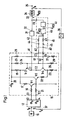
- 10 denotes a reference oscillator, which supplies a preferably quartz-stabilized reference frequency f R to a first input 11 of a phase comparison circuit 12.
- a first output 13 and a second output 14 of the phase comparison circuit 12 are each connected to an input E1 and E2 of a controllable voltage pulse / current pulse converter 15, which corresponds to the left-hand circuit part framed in FIG. 1 by dashed lines.
- the input E1 is connected via a first resistor 16 to the base of a first transistor Tr1 of npn type, the emitter of which is connected to ground and the collector of which is connected to the emitter of a third transistor Tr3 via a second resistor 17 of the pnp type and via a third resistor 19 is connected to a node 20 positive operating potential U R.
- the second input E2 of the controllable voltage pulse / current pulse converter 15 is connected via a fourth resistor 21 to the base of a second transistor Tr2 of the NPN type, the collector of which is located at the node 20.
- the emitter of the second transistor Tr2 is connected via a fifth resistor 22 to the emitter of a fourth npn transistor Tr4 and via a sixth resistor 23 to ground.
- the collector of the fourth transistor Tr4 is connected to the collector of the third transistor Tr3.
- the base of the third transistor Tr3 is connected to the circuit point 20 via a first diode 24 and a seventh resistor 25 connected in series therewith, also directly to a third input E3 and via an eighth resistor 26 to ground.
- the base of the fourth transistor Tr4 leads directly to a fourth input E4 of the controllable voltage pulse / current pulse converter 15, also via a second diode 27 and a resistor 28 in series therewith to ground and finally via a resistor 29 to the node 20
- Output A1 of the controllable voltage pulse / current pulse converter 15 is connected directly to the collectors of the third and fourth transistors Tr3 and Tr4.
- a loop filter 31 connects to the output A1, the output 32 of which is connected to a control input 33 of a voltage-controlled oscillator 34.
- An output 35 of the voltage-controlled oscillator 34 is also the output of the single-loop PLL circuit.
- the output 35 is connected via an adjustable frequency divider 36 to a second input 37 of the phase comparison circuit 12.
- the single-loop PLL circuit described above corresponds to a known circuit with two controllable current sources.
- the feedback circuit 40 denotes a feedback circuit, by which the known circuit is supplemented in order to obtain a single-loop PLL circuit with a particularly short latching time.
- the feedback circuit 40 has an input E5 and two outputs A2 and A3.
- the input ES is connected to the output 32 of the loop filter 31. It is connected to an isolating amplifier 41 with a high-resistance input and two parallel branches each a resistor 42 and 43 and a respective capacitor 44 and 45 connected in series with each of the outputs A2 and A3 in connection.
- the inputs E3 and E4 of the controllable current source 15 connect to the outputs A2 and A3.
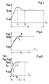
- the single-loop PLL circuit with the frequency divider 36 can be switched to output frequencies f A in a frequency range of, for example, 890 to 915 MHz. It is further assumed that the single-loop PLL circuit is locked, for example, at a first frequency f A1 of 890 MHz.
- the control voltage U VCO for the voltage controlled oscillator 34 then has a value U 1 VCO (Fig. 3), which corresponds to the first frequency f A1 .
- the frequency divider 36 is now switched over in such a way that a second output frequency f A2 of, for example, 915 MHz is to be obtained, the reference frequency f R of, for example, 200 kHz and the comparison frequency f V obtained by dividing the output frequency f A into frequency and Phase no longer coincides.
- the phase comparison circuit 12 therefore outputs negative pulses at its output 13 ( ⁇ V) (FIG. 2C), the pulse widths b1, b2 ... of which depend on the respective frequency or phase deviation between the reference frequency f R and the comparison frequency f V .
- the second output 14 ( ⁇ R) delivers approximately needle-shaped pulses i1 and i2 at the same time; see. Figure 2D.
- the controllable voltage pulse / current pulse converter 15 is driven, and the transistors Tr1 and Tr2 are driven via the resistors 16 and 21, the negative pulses at the output 13 of the phase comparison circuit 12 (see FIG. 2C) transistor Tr1 block and thus turn on the power source with transistor Tr3.
- This current source then delivers current pulses 11 at its output A1 which correspond to the voltage pulses in FIG. 2C.
- the loop filter 31 From the current pulses 11, the loop filter 31 generates the voltage curve U VCO shown in FIG. 3, starting from the control voltage U 1 U 1 VCO, as a function from time t.
- the voltage U VCO controls the frequency of the voltage controlled oscillator 34 in the direction of higher frequencies.
- the control voltage U VCO After several current pulses I1, that is to say at a point in time t1 (FIG. 3), the control voltage U VCO has reached a maximum, that is to say a voltage value which is above the control voltage U2 VCO for the second output frequency f A2 . Then the output 14 ( ⁇ R) of the phase comparison circuit 12 supplies voltage pulses i3, i4 which are wider than the needle-shaped pulses i1, i2. During the pulse durations of the pulses i3, i4 ..., the second transistor Tr2 is blocked and the current source with the transistor Tr4 is released. It then delivers current pulses I2 of opposite polarity as I1 to the loop filter 31, and as long as, until a time t2 a voltage minimum is reached, etc.
- the PLL circuit is now engaged.
- the controllable feedback circuit 40 (FIG. 1) is required.
- the control voltage U VCO is tapped at the output 32 of the loop filter 31 and fed to the high-resistance input of the isolating amplifier 41.
- the amplified control voltage U ' VCO at the output of the isolation amplifier 41 is via the RC elements 42, 44; 43, 45 to the control inputs E3, E4 of the controllable voltage pulse / current pulse converter 15, at which the voltages U1 and U2 are located.
- a further shortening of the latching time is achieved if a phase shifter 46 is connected downstream of the isolating amplifier 41 in FIG. 1.
- the control voltage U ' VCO results in a phase-shifted voltage U " VCO ; curve profile Y in FIG. 5.
- the voltage U1 or U2 is influenced only after the time T ⁇ has elapsed, and the phase shift is selected such that the influence takes place approximately after two thirds of the difference between the voltages U2 VCO and U1 VCO .
Landscapes
- Stabilization Of Oscillater, Synchronisation, Frequency Synthesizers (AREA)
Applications Claiming Priority (2)
| Application Number | Priority Date | Filing Date | Title |
|---|---|---|---|
| DE4008245A DE4008245A1 (de) | 1990-03-15 | 1990-03-15 | Einschleifen-pll-schaltung |
| DE4008245 | 1990-03-15 |
Publications (3)
| Publication Number | Publication Date |
|---|---|
| EP0446571A2 true EP0446571A2 (fr) | 1991-09-18 |
| EP0446571A3 EP0446571A3 (en) | 1991-11-27 |
| EP0446571B1 EP0446571B1 (fr) | 1995-05-03 |
Family
ID=6402242
Family Applications (1)
| Application Number | Title | Priority Date | Filing Date |
|---|---|---|---|
| EP91100299A Expired - Lifetime EP0446571B1 (fr) | 1990-03-15 | 1991-01-11 | Circuit PLL à boucle unique |
Country Status (3)
| Country | Link |
|---|---|
| EP (1) | EP0446571B1 (fr) |
| AT (1) | ATE122187T1 (fr) |
| DE (2) | DE4008245A1 (fr) |
Family Cites Families (2)
| Publication number | Priority date | Publication date | Assignee | Title |
|---|---|---|---|---|
| US3906375A (en) * | 1974-02-08 | 1975-09-16 | Rockwell International Corp | Constant gain switching amplifier apparatus |
| GB2143385A (en) * | 1983-07-13 | 1985-02-06 | Plessey Co Plc | Phase lock loop circuit |
-
1990
- 1990-03-15 DE DE4008245A patent/DE4008245A1/de not_active Withdrawn
-
1991
- 1991-01-11 AT AT91100299T patent/ATE122187T1/de active
- 1991-01-11 DE DE59105351T patent/DE59105351D1/de not_active Expired - Fee Related
- 1991-01-11 EP EP91100299A patent/EP0446571B1/fr not_active Expired - Lifetime
Also Published As
| Publication number | Publication date |
|---|---|
| EP0446571B1 (fr) | 1995-05-03 |
| DE4008245A1 (de) | 1991-09-19 |
| EP0446571A3 (en) | 1991-11-27 |
| ATE122187T1 (de) | 1995-05-15 |
| DE59105351D1 (de) | 1995-06-08 |
Similar Documents
| Publication | Publication Date | Title |
|---|---|---|
| DE1562321C3 (de) | Schaltungsanordnung zur Umsetzung eines Eingangssignals in breitenmodulierte Impulse als Ausgangssignal | |
| DE3232155C2 (de) | Schaltungsanordnung zur Regelung der Phasendifferenz zwischen einem Eingangssignal und einem Ausgangssignal | |
| DE2912171C2 (de) | Als Schaltregler arbeitender Gleichspannungswandler | |
| DE3100429C2 (de) | Schaltungsanordnung zur Regelung der Phasendifferenz zwischen einem Referenzsignal und einem Ausgangssignal | |
| EP0954902B1 (fr) | Generateur d'impulsions hyperfrequences | |
| DE2603641A1 (de) | Phasenstarre rueckfuehrschleife, insbesondere fuer einen breitbandsender | |
| DE1516734B1 (de) | Mehrkanal-Sender-Empfaenger | |
| DE2836288C2 (de) | Kombi-Tuner | |
| DE2943510C2 (de) | Phasengeregelter Hochfrequenzoszillator | |
| DE3751078T2 (de) | Quartz-Oszillator mit breitem Ziehbereich. | |
| DE2624133C3 (de) | Mischeranordnung | |
| DE60114733T2 (de) | Phasenregelschleife mit verringerter Verriegelungszeit | |
| DE2154869A1 (de) | Schaltungsanordnung zur Erzeugung von Schwingungen | |
| EP0446571B1 (fr) | Circuit PLL à boucle unique | |
| DE2802981A1 (de) | Mit phasensynchronisierter schleife arbeitende abstimmeinrichtung | |
| DE3905860C2 (fr) | ||
| DE10009079B4 (de) | Piezoelektrischer Oszillator | |
| DE1813734A1 (de) | Phasengesteuertes Oszillatorsystem mit variabler Verstaerkung in der Phasensteuerschleife | |
| DE2044635C3 (de) | Schaltung zum automatischen Sendersuchlauf in Rundfunkempfängern | |
| DE1140969B (de) | Frequenzregelschaltung zur Synchronisierung eines Oszillators | |
| DE3319943C2 (de) | Hochfrequenz-Impulsverstärker | |
| EP0014387B1 (fr) | Oscillateur piézo-électrique à large bande à commande électrique de fréquence | |
| DE60004411T2 (de) | Schwingschaltung mit breitem Dynamikbereich | |
| DE2129129C3 (fr) | ||
| DE1951767C3 (de) | Signalgenerator |
Legal Events
| Date | Code | Title | Description |
|---|---|---|---|
| PUAI | Public reference made under article 153(3) epc to a published international application that has entered the european phase |
Free format text: ORIGINAL CODE: 0009012 |
|
| AK | Designated contracting states |
Kind code of ref document: A2 Designated state(s): AT DE DK FR GB IT NL SE |
|
| PUAL | Search report despatched |
Free format text: ORIGINAL CODE: 0009013 |
|
| AK | Designated contracting states |
Kind code of ref document: A3 Designated state(s): AT DE DK FR GB IT NL SE |
|
| RAP3 | Party data changed (applicant data changed or rights of an application transferred) |
Owner name: ROBERT BOSCH GMBH |
|
| 17P | Request for examination filed |
Effective date: 19920511 |
|
| 17Q | First examination report despatched |
Effective date: 19940121 |
|
| GRAA | (expected) grant |
Free format text: ORIGINAL CODE: 0009210 |
|
| AK | Designated contracting states |
Kind code of ref document: B1 Designated state(s): AT DE DK FR GB IT NL SE |
|
| PG25 | Lapsed in a contracting state [announced via postgrant information from national office to epo] |
Ref country code: GB Effective date: 19950503 Ref country code: FR Effective date: 19950503 Ref country code: DK Effective date: 19950503 Ref country code: NL Free format text: LAPSE BECAUSE OF FAILURE TO SUBMIT A TRANSLATION OF THE DESCRIPTION OR TO PAY THE FEE WITHIN THE PRESCRIBED TIME-LIMIT Effective date: 19950503 Ref country code: IT Free format text: LAPSE BECAUSE OF FAILURE TO SUBMIT A TRANSLATION OF THE DESCRIPTION OR TO PAY THE FEE WITHIN THE PRESCRIBED TIME-LIMIT;WARNING: LAPSES OF ITALIAN PATENTS WITH EFFECTIVE DATE BEFORE 2007 MAY HAVE OCCURRED AT ANY TIME BEFORE 2007. THE CORRECT EFFECTIVE DATE MAY BE DIFFERENT FROM THE ONE RECORDED. Effective date: 19950503 |
|
| REF | Corresponds to: |
Ref document number: 122187 Country of ref document: AT Date of ref document: 19950515 Kind code of ref document: T |
|
| REF | Corresponds to: |
Ref document number: 59105351 Country of ref document: DE Date of ref document: 19950608 |
|
| PG25 | Lapsed in a contracting state [announced via postgrant information from national office to epo] |
Ref country code: SE Effective date: 19950803 |
|
| EN | Fr: translation not filed | ||
| NLV1 | Nl: lapsed or annulled due to failure to fulfill the requirements of art. 29p and 29m of the patents act | ||
| GBV | Gb: ep patent (uk) treated as always having been void in accordance with gb section 77(7)/1977 [no translation filed] |
Effective date: 19950503 |
|
| PG25 | Lapsed in a contracting state [announced via postgrant information from national office to epo] |
Ref country code: AT Effective date: 19960111 |
|
| PLBE | No opposition filed within time limit |
Free format text: ORIGINAL CODE: 0009261 |
|
| STAA | Information on the status of an ep patent application or granted ep patent |
Free format text: STATUS: NO OPPOSITION FILED WITHIN TIME LIMIT |
|
| 26N | No opposition filed | ||
| PGFP | Annual fee paid to national office [announced via postgrant information from national office to epo] |
Ref country code: DE Payment date: 20020318 Year of fee payment: 12 |
|
| PG25 | Lapsed in a contracting state [announced via postgrant information from national office to epo] |
Ref country code: DE Free format text: LAPSE BECAUSE OF NON-PAYMENT OF DUE FEES Effective date: 20030801 |