EP0444396B1 - Kontaktiereinrichtung für ein SI-Modul - Google Patents
Kontaktiereinrichtung für ein SI-Modul Download PDFInfo
- Publication number
- EP0444396B1 EP0444396B1 EP91100054A EP91100054A EP0444396B1 EP 0444396 B1 EP0444396 B1 EP 0444396B1 EP 91100054 A EP91100054 A EP 91100054A EP 91100054 A EP91100054 A EP 91100054A EP 0444396 B1 EP0444396 B1 EP 0444396B1
- Authority
- EP
- European Patent Office
- Prior art keywords
- contact elements
- contacts
- card
- contact
- contacting apparatus
- Prior art date
- Legal status (The legal status is an assumption and is not a legal conclusion. Google has not performed a legal analysis and makes no representation as to the accuracy of the status listed.)
- Expired - Lifetime
Links
Images
Classifications
-
- G—PHYSICS
- G06—COMPUTING OR CALCULATING; COUNTING
- G06K—GRAPHICAL DATA READING; PRESENTATION OF DATA; RECORD CARRIERS; HANDLING RECORD CARRIERS
- G06K7/00—Methods or arrangements for sensing record carriers, e.g. for reading patterns
- G06K7/0013—Methods or arrangements for sensing record carriers, e.g. for reading patterns by galvanic contacts, e.g. card connectors for ISO-7816 compliant smart cards or memory cards, e.g. SD card readers
- G06K7/0021—Methods or arrangements for sensing record carriers, e.g. for reading patterns by galvanic contacts, e.g. card connectors for ISO-7816 compliant smart cards or memory cards, e.g. SD card readers for reading/sensing record carriers having surface contacts
Definitions
- the invention relates to a contacting device, in particular for an SI module.
- SIM Subscriber Identity Module
- H it is an electronic element, for example an integrated circuit, which provides information about the identity of a subscriber, for example on a telephone system.
- the contact pattern of such a module corresponds to that of the IC card according to ISO 7816, while the external dimensions of the SIM are considerably smaller, namely 25 mm x 15 mm compared to 85.5 mm x 54 mm.
- the invention aims in particular to develop a contacting device for a SIM, the external dimensions of this contacting device should only slightly exceed the dimensions of the SIM.
- the thickness of the contacting device should preferably be less than 3 mm.
- the contact forces should be equal to or greater than the contacting devices for the larger IC cards.
- a switch should preferably be provided which closes or opens after the so-called read contacts of the contacting device have been put on. Furthermore, for certain applications, contacting should be possible without relative movement between the reader and the SIM card.
- the known contacting devices for conventional IC cards exceed either the length or the height of the required dimensions, since they require the same contact forces between 0.2 and 0.4 N, without limitation of the external dimensions.
- the boundary conditions of contact force and spring travel result in spring elements which, in a conventional arrangement, meet the requirements Exceed dimensions.
- the present invention provides a contacting device according to claim 1.
- the contacting device according to the invention has the advantage that the contact pitch is halved, thereby reducing the length by the row spacing.
- a cover of the contacting device can be designed as a card holder.
- the contacting device according to the invention for an SI module is in the so-called mobile phones.
- the contacting device could be installed in the mobile phone and the information relating to the subscriber would be read out of the SI module by the contacting device.
- FR-A-2 633 754 shows a contacting device with a contact block in which contact rods are arranged. These protrude, partially arranged in interlocking fashion, from the contact block upwards or through holes in the contact block downwards.
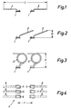
- Fig. 1 two SI module or card contacts 1 are shown, which are contacted by contact elements 2. This known contact arrangement means that the permissible length L has been exceeded.
- FIG. 4 shows the top view of a card receiving chamber 4, which has cutouts 5 in the area of which contact elements 6 end, namely for contacting the module contacts 1 (not shown here), the predetermined row spacing being designated by 7.
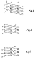
- connection ends 9 are arranged opposite one another here.
- FIG. 6 shows a further embodiment according to the invention, different contact elements 10, 11 being used for the rows A and B here.
- the connection ends of the contact elements are on the same side here.
- Fig. 7 also shows an arrangement which is particularly suitable for surface mounting (SMT), here again a one-sided connection is provided for the contact elements 12, 13.
- SMT surface mounting
- contact arrangements provided according to the invention are particularly intended for SI modules, particularly short contacting devices for IC cards can also be realized with the arrangement according to the invention.
- the relatively short contact springs only allow a small spring travel. It is therefore difficult to implement a switch that is actuated after the reading or card contacts have been contacted.
- a solution according to the invention provides for a switch to be actuated with the locking element for the cards.
- the purpose of this switch is to indicate that the reading status has been reached.
- the cover for pressing the SIM card is put on, so that the switch is actuated with certainty after reaching the reading position.
- the lid can also be used as a card case.
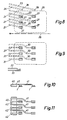
- FIG. 8 shows an embodiment of the invention with connection ends on the same side for the contact elements 20, 21 and also for the switch contact elements 23 and 24.
- the SIM card or its receiving opening is indicated at 25.
- the axis of a pivotable cover, not shown, is designated by 26, the inwardly projecting contact ends of the contact elements 23 and 24 lying in the region of the cover, not shown, which on the one hand the card with its contacts or zones 1 against the contacts 27 of the contact elements 20 , 21 presses and finally connects the two contact ends 28 of the contacts 23, 24 at the end of the pivoting movement, for example by a metallic strip in the cover.
- the switch formed by the contact elements 23, 24 consists of the same contact elements as the read contacts, in FIG. 9 the switch is constructed from a pair of modulated read contacts 32, 33. 9, the contact elements 30, 31 are also formed in the manner shown. In the arrangement according to FIG. 9, the actuation of the switch does not require a conductive strip or the like in the cover.
- FIGS. 10 and 11 show a further exemplary embodiment of the invention in which the SIM schematically represented by its contact zones 1 is contacted via contact elements 41, 42, the contact elements 41, 42 being guided around an insulating part 40 in order to form contact points there that form a contact point enable a high number of mating cycles.
Landscapes
- Engineering & Computer Science (AREA)
- Artificial Intelligence (AREA)
- Computer Vision & Pattern Recognition (AREA)
- Physics & Mathematics (AREA)
- General Physics & Mathematics (AREA)
- Theoretical Computer Science (AREA)
- Coupling Device And Connection With Printed Circuit (AREA)
Description
- Die Erfindung bezieht sich auf eine Kontaktiereinrichtung und zwar insbesondere für ein SI-Modul.
- Das Wort "SIM" steht für "Subscriber Identity Module", d. h. es handelt sich hier um ein elektronisches Element beispielsweise eine integrierte Schaltung, die über die Identität eines Teilnehmers beispielsweise an einem Telefonsystem Auskunft gibt. Das Kontaktbild eines solchen Moduls entspricht dem der IC-Karte nach ISO 7816, während die Außenmaße des SIM erheblich kleiner sind, und zwar 25 mm x 15 mm gegenüber 85,5 mm x 54 mm.
- Die Erfindung bezweckt insbesondere eine Kontaktiervorrichtung für ein SIM zu entwickeln, wobei die Außenmaße dieser Kontaktiervorrichtung die Abmessungen des SIM nur unwesentlich übersteigen sollen. Die Dicke der Kontaktiervorrichtung soll vorzugsweise kleiner sein als 3 mm. Ferner sollen die Kontaktkräfte gleich oder größer sein als bei den Kontaktiervorrichtungen für die größeren IC-Karten. Weiterhin soll vorzugsweise ein Schalter vorzusehen sein, der nach dem Aufsetzen der sogenannten Lesekontakte der Kontaktiervorrichtung schließt oder öffnet. Ferner soll für bestimmte Anwendungsfälle eine Kontaktierung ohne Relativbewegung zwischen Leser und SIM-Karte realisierbar sein.
- Die bekannten Kontaktiervorrichtungen für herkömmliche IC-Karten überschreiten entweder die Länge oder die Höhe der geforderten Maße, da sie gleiche Kontaktkräfte zwischen 0,2 und 0,4 N fordern, ohne Begrenzung der Außenmaße. Aus den Grenzbedingungen von Kontaktkraft und Federweg (zusammengesetzt aus Toleranzen von Kartendicke und Fertigungsgenauigkeit), ergeben sich Federelemente, die bei herkömmlicher Anordnung die geforderten Maße überschreiten.
- Die vorliegende Erfindung sieht zur Vermeidung der Nachteile des Standes der Technik eine Kontaktiereinrichtung gemäß Anspruch 1 vor. Die erfindungsgemäße Kontaktiereinrichtung hat dem Vorteil, daß die Kontaktteilung halbiert ist und dadurch die Länge um den Reihenabstand reduziert.
- Ein Deckel der Kontaktiereinrichtung kann als Kartenhalter ausgebildet sein.
- Ein Anwendungsgebiet der erfindungsgemäßen Kontaktiereinrichtung für ein SI-Modul besteht bei den sogenannten Mobiltelefonen. Hier könnte die Kontaktiereinrichtung im Mobiltelefon eingebaut sein und die den Teilnehmer betreffende Information würde durch die Kontaktiereinrichtung aus dem SI-Modul ausgelesen werden.
- FR-A-2 633 754 zeigt eine Kontaktiereinrichtung mit einem Kontaktblock in dem Kontaktstangen angeordnet sind. Diese ragen, teilweise in einandergreifend angeordnet vom Kontaktblock aus nach oben bzw. durch Löcher im Kontaktblock nach unten.
- Weiter Vorteile, Ziele und Einzelheiten der Erfindung ergeben sich aus der Beschreibung von Ausführungsbeispielen anhand der Zeichnungen; die Zeichnungen zeigen:
- Fig. 1
- schematisch zwei Kontaktelemente für eine herkömmliche Chipkarte;
- Fig. 2
- schematisch eine andere Anordnung der Kontaktelemente;
- Fig. 3
- eine weitere schematische Anordnung der Kontaktelement;
- Fig. 4
- die Anordnung der Kontaktelemente gemäß Fig. 1 für eine Kontaktiereinrichtung für ein SI-Modul;
- Fig. 5
- schematisch die bevorzugte Anordnung von Kontakten für die Kontaktiervorrichtung für ein SI-Modul;
- Fig. 6
- eine andere bevorzugte Anordnung der Kontakte für einseitigen Konaktanschluß;
- Fig. 7
- eine weitere bevorzugte Anordnung der Kontakte für insbesondere Oberflächenmontage und einseitigen Kontaktanschluß;
- Fig. 8
- die erfindungsgemäße Anordnung von Kontakten zusammen mit einem Schalter;
- Fig. 9
- eine weitere bevorzugte Anordnung von Kontakten zusammen mit einem Schalter;
- Fig. 10
- schematisch in Seitenansicht die Verbindung eines SIM mit einem Steckelement;
- Fig. 11
- eine Draufsicht auf die Anordnung gemäß Fig. 10.
- In Fig. 1 sind zwei SI-Modul- oder Kartenkontakte 1 dargestellt, die durch Kontaktelemente 2 kontaktiert werden. Diese bekannte Kontaktanordnung bedeutet eine Überschreitung der zulässigen Länge L.
- Bei der Anordnung gemäß Fig. 2 wird die zulässige Höhe H überschritten.
- Das gleiche gilt auch für die Anordnung der Kontakte 3 gemäß Fig. 3.
- In Fig. 4 ist die Draufsicht auf eine Kartenaufnahmekammer 4 dargestellt, die Ausschnitte 5 besitzt in deren Bereich Kontaktelemente 6 enden und zwar zur Kontaktierung mit den hier nicht gezeigten Modulkontakten 1, wobei der vorgegebene Reihenabstand mit 7 bezeichnet ist.
- Fig. 5 zeigt ähnlich wie Fig. 4 eine bevorzugte Anordnung der Kontaktelemente 8, gemäß welcher die Kontaktteilung halbiert ist um dadurch die Länge L um den Reihenabstand 7 zu reduzieren.
Man erkennt, daß die Kontakte für die Reihe A zwischen der Reihe B hindurchgeführt werden und umgekehrt. Für Reihe A und auch für die Reihe B können die gleichen Kontakte oder -elemente 8 Verwendung finden, was fertigungstechnisch vorteilhaft ist. Die Anschlußenden 9 sind hier gegenüber liegend angeordnet. - Fig. 6 zeigt eine weitere erfindungsgemäße Ausgestaltung, wobei hier unterschiedliche Kontaktelemente 10, 11 für die Reihen A und B Verwendung finden. Die Anschlußenden der Kontaktelemente liegen hier auf der gleichen Seite.
- Fig. 7 zeigt ferner eine Anordnung, die besonders für die Oberflächenmontage (SMT) geeignet ist, wobei hier wiederum ein einseitiger Anschluß für die Kontaktelemente 12, 13 vorgesehen ist.
- Obwohl die gemäß der Erfindung vorgesehenen Kontaktanordnungen besonders für SI-Module vorgesehen sind, so können doch mit der erfindungsgemäßen Anordnung auch besonders kurze Kontaktiereinrichtungen für IC-Karten realisiert werden.
- Die relativ kurzen Kontaktfedern erlauben nur einen kleinen Federweg. Eine Nacheilung eines Schalters der nach dem Kontakieren der Lese- oder Kartenkontakte betätigt wird, ist somit schwer realisierbar.
- Eine erfindungsgemäße Lösung sieht vor einen Schalter mit dem Verriegelungselement für die Karten zu betätigen. Dieser Schalter hat den Zweck das Erreichen des Lesezustandes anzuzeigen.
- Erfindungsgemäß wird beispielsweise der Deckel zum Andrücken der SIM-Karte aufgesetzt, sodaß der Schalter mit Sicherheit nach Erreichen der Leseposition betätigt wird. Außerdem kann der Deckel als Kartenetui dienen.
- Fig. 8 zeigt eine Ausgestaltung der Erfingung mit auf der gleichen Seite liegenden Anschlußenden für die Kontaktelemente 20, 21 und auch für die Schalterkontaktelemente 23 und 24. Die SIM-Karte oder deren Aufnahmeöffnung ist bei 25 angedeutet. Mit 26 ist die Achse eines schwenkbaren nicht dargestellten Deckels bezeichnet, wobei die nach innen ragenden Kontaktenden der Kontaktelemente 23 und 24 im Bereich des nicht gezeigten Deckels liegen, der zum einen die Karte mit ihren Kontakten oder -zonen 1 gegen die Kontakte 27 der Kontaktelemente 20, 21 drückt und schließlich am Ende der Schwenkbewegung die beiden Kontaktenden 28 der Kontakte 23, 24 verbindet, beispielsweise durch einen metallischen Streifen im Deckel.
- Während beim Ausführungsbeispiel gemäß Fig. 8 der durch die Kontaktelemente 23, 24 gebildete Schalter aus den gleichen Kontaktelementen wie die Lesekontakte besteht, ist bei Fig. 9 der Schalter aus einem Paar modulifizierter Lesekontakte 32, 33 aufgebaut. In Fig. 9 sind ferner die Kontaktelemente 30, 31 in der dargestellten Weise ausgebildet. Bei der Anordnung gemäß Fig. 9 erfordert die Betätigung des Schalters keinen leitenden Streifen oder dergleichen im Deckel.
- Die Fig. 10 und 11 zeigen ein weiteres Ausführungsbeispiel der Erfindung bei dem das durch seine Kontaktzonen 1 schematisch dargestellte SIM über Kontaktelemente 41, 42 kontaktiert ist, wobei die Kontaktelemente 41, 42 um ein Isolierteil 40 herumgeführt sind um dort Kontaktstellen zu bilden, die eine hohe Steckzyklenzahl ermöglichen.
Claims (6)
- Kontaktiereinrichtung für in zwei Kontaktreihen (A, B) angeordnete Kartenkontakte (1) insbesondere die einer SIM-Karte wobeiKontaktelemente (8; 20, 21) der Kontaktiereinrichtung für die die beiden Kontaktreihen (A, B) nebeneinander liegen,wobei die Kontaktelemente (8; 20, 21) für die eine Reihe (A) zwischen denen für die andere Reihe (B) hindurchgeführt werden und umgekehrt, undwobei die Kontaktelemente (8; 20, 21) für die Reihen (A, B) gleichlang sind und ihre Anschlußenden (9) auf entgegengesetzten Seiten liegen.
- Kontaktiereinrichtung nach Anspruch 1, dadurch gekennzeichnet, daß ein Schalter vorgesehen ist, der nach dem Aufsetzen der Kontaktelemente öffnet oder schließt und der vorzugsweise mit den Kontaktelementen gleiche Kontaktelemente (23, 24) verwendet.
- Kontaktiereinrichtung nach einem der vorhergehenden Ansprüche, dadurch gekennzeichnet, daß der Schalter von einem Verriegelungselement beispielsweise von einem Deckel für die Karte betätigt wird.
- Kontaktiereinrichtung nach Ansprüch 3, dadurch gekennzeichnet, daß das Verriegelungselement gleichzeitig als Kartenetui dient und dabei Schutz gegen Beschädigung und Verlust bietet.
- Kontaktiereinrichtung nach Ansprüch 3 oder 4, dadurch gekennzeichnet, daß das Verriegelungselement nach dem Lötprozeß der Kontaktelemente eingesetzt ist.
- Kontaktiereinrichtung nach einem der vorhergehenden Ansprüche, dadurch gekennzeichnet, daß die Kontaktelemente (41, 42) um ein Isolierstück (40) herumgeführt sind und so die Kontaktstellen für hohe Steckzyklenzahlen bilden.
Applications Claiming Priority (2)
| Application Number | Priority Date | Filing Date | Title |
|---|---|---|---|
| DE4002680 | 1990-01-30 | ||
| DE4002680 | 1990-01-30 |
Publications (3)
| Publication Number | Publication Date |
|---|---|
| EP0444396A1 EP0444396A1 (de) | 1991-09-04 |
| EP0444396B1 true EP0444396B1 (de) | 1997-07-09 |
| EP0444396B2 EP0444396B2 (de) | 2000-11-02 |
Family
ID=6399060
Family Applications (1)
| Application Number | Title | Priority Date | Filing Date |
|---|---|---|---|
| EP91100054A Expired - Lifetime EP0444396B2 (de) | 1990-01-30 | 1991-01-02 | Kontaktiereinrichtung für ein SI-Modul |
Country Status (4)
| Country | Link |
|---|---|
| US (1) | US5269707A (de) |
| EP (1) | EP0444396B2 (de) |
| JP (1) | JP2574710B2 (de) |
| DE (1) | DE59108764D1 (de) |
Families Citing this family (40)
| Publication number | Priority date | Publication date | Assignee | Title |
|---|---|---|---|---|
| DE4243076C2 (de) * | 1992-12-18 | 2000-08-31 | Amphenol Tuchel Elect | Kotaktiereinrichtung für eine Chipkarte |
| EP0698247B1 (de) * | 1993-05-14 | 1998-09-02 | AMPHENOL-TUCHEL ELECTRONICS GmbH | Smt-leser für sim- und standardkarten |
| US5726432A (en) * | 1993-05-14 | 1998-03-10 | Amphenol-Tuchel Electronics Gmbh | Contacting system or reader for chip cards |
| FR2709850A1 (fr) * | 1993-09-06 | 1995-03-17 | Hopt & Schuler Ddm | Dispositif à ressort de contact pour cartes et son procédé de fabrication. |
| FR2714539B1 (fr) * | 1993-12-24 | 1996-01-26 | Itt Composants Instr | Connecteur électrique pour le raccordement d'une carte à mémoire électronique. |
| US5791942A (en) * | 1994-01-11 | 1998-08-11 | Stewart Connector Systems, Inc. | High frequency electrical connector |
| US5639266A (en) | 1994-01-11 | 1997-06-17 | Stewart Connector Systems, Inc. | High frequency electrical connector |
| US5496180A (en) * | 1994-04-06 | 1996-03-05 | The Whitaker Corporation | Surface mountable card edge connector |
| GB9412358D0 (en) * | 1994-06-20 | 1994-08-10 | Amp Holland | SIM card connector |
| DE19521360C2 (de) * | 1994-11-08 | 1999-07-29 | Amphenol Tuchel Elect | Kartenlesegerät insbesondere SIM-Kartenleser |
| US5667408A (en) * | 1994-12-01 | 1997-09-16 | The Whitaker Corporation | Smart card connector with preloaded data contacts |
| DE19506606C2 (de) * | 1995-02-24 | 1996-12-19 | Amphenol Tuchel Elect | Chipkartenleser |
| DE19508363C1 (de) * | 1995-03-10 | 1996-07-25 | Amphenol Tuchel Elect | Aufnahmegehäuse für eine Chipkarte |
| DE19516987A1 (de) * | 1995-05-09 | 1996-11-14 | Amphenol Tuchel Elect | Kartenlesevorrichtung für Chipkarten und/oder SIM-Karten mit unterschiedlicher Dicke |
| US5714742A (en) * | 1995-05-10 | 1998-02-03 | Matsushita Electric Industrial Co., Ltd. | IC-card reader/writer for an IC-card |
| DE19521721B4 (de) * | 1995-06-14 | 2006-12-07 | Amphenol-Tuchel Electronics Gmbh | Geschirmte Kontaktiereinrichtung |
| DE19634565C1 (de) * | 1996-08-27 | 1997-11-06 | Amphenol Tuchel Elect | Kontaktträger |
| DE19638622A1 (de) * | 1996-09-20 | 1998-03-26 | Amphenol Tuchel Elect | Chipkarten-Kontaktiergerät |
| EP0840246B2 (de) * | 1996-11-05 | 2011-03-16 | Amphenol-Tuchel Electronics GmbH | SIM-Kartenkontaktiervorrichtung |
| US6112994A (en) * | 1997-02-27 | 2000-09-05 | The Whitaker Corporation | Card reader connector with attachable cover |
| US7079778B1 (en) * | 2000-04-07 | 2006-07-18 | Northrop Grumman Corporation | Rugged shock-resistant backplane for embedded systems |
| IL139807A0 (en) | 1998-06-02 | 2002-02-10 | Stewart Connector Systems Inc | High frequency electrical connector assembly such as multi-port multi-level connector assembly |
| FR2780532B1 (fr) * | 1998-06-26 | 2001-12-07 | Framatome Connectors Int | Connecteur pour mini-carte a faible profil |
| US6062887A (en) * | 1998-08-31 | 2000-05-16 | Motorola, Inc. | Electronic device with dual card reader employing a drawer |
| DE59902367D1 (de) * | 1998-09-22 | 2002-09-19 | Siemens Ag | Verfahren und vorrichtung zum prüfen der zugangsberechtigung zu einem system |
| EP1030260B1 (de) | 1999-02-16 | 2007-11-14 | AMPHENOL-TUCHEL ELECTRONICS GmbH | Ein chipkarten-verbinder |
| FI991002L (fi) * | 1999-05-03 | 2000-11-04 | Nokia Mobile Phones Ltd | Toimikorttiliitin ja matkaviestin |
| JP2001015194A (ja) | 1999-05-05 | 2001-01-19 | Thomas & Betts Corp <T&B> | プリント配線板から持ち上げた配置で使用する改良型スマート・カード読取器 |
| DE19935188C2 (de) * | 1999-07-27 | 2002-06-13 | Amphenol Tuchel Elect | Kontaktblock für einen Chipkartenleser |
| USD456407S1 (en) | 1999-12-29 | 2002-04-30 | Tyco Electronics Logistics Ag | Stacked smart card reader |
| USD454875S1 (en) | 1999-12-29 | 2002-03-26 | Tyco Electronics Logistics Ag | Single smart card reader |
| US6942154B1 (en) | 2000-02-24 | 2005-09-13 | Matsushita Electric Industrial Co, Ltd. | Card connector and portable telephone having the same |
| US6508673B2 (en) | 2000-04-05 | 2003-01-21 | Mcdowell Jennifer Lyn | Low cost smart card reader, extension style, with wiping contacts |
| JP3899221B2 (ja) * | 2000-07-06 | 2007-03-28 | アルプス電気株式会社 | カード用コネクタ装置 |
| US6346010B1 (en) | 2000-08-10 | 2002-02-12 | The Wiremold Company | Modular connector |
| FR2843654B1 (fr) * | 2002-08-13 | 2006-03-03 | Itt Mfg Entpr S Inc | Agencement pour le raccordement electrique d'un composant sur la face superieure d'une plaque a circuits imprimes |
| DE102005061641A1 (de) * | 2005-12-22 | 2007-06-28 | Amphenol-Tuchel-Electronics Gmbh | Smart Card Connector mit landenden Kontakten und Deckelfeder als Kartenbremse |
| US8235978B2 (en) * | 2007-11-01 | 2012-08-07 | Valens Associated Inc. | Thermal capsulotomy tool and system |
| WO2009100296A1 (en) * | 2008-02-08 | 2009-08-13 | Panduit Corp. | Communications connector with improved contacts |
| DE102014105502B4 (de) * | 2014-04-17 | 2016-09-08 | Amphenol-Tuchel Electronics Gmbh | Chipkartenleser zur Signalübertragung |
Family Cites Families (18)
| Publication number | Priority date | Publication date | Assignee | Title |
|---|---|---|---|---|
| GB1382691A (en) † | 1972-06-17 | 1975-02-05 | Amp Inc | Electrical connectors and their method of manufacture |
| JPS5826152B2 (ja) * | 1980-11-14 | 1983-06-01 | 日本電信電話株式会社 | 多極コネクタ |
| JPS5960523A (ja) * | 1982-09-30 | 1984-04-06 | Canon Inc | 電子機器 |
| DE3343757A1 (de) † | 1983-12-02 | 1985-06-13 | Siemens AG, 1000 Berlin und 8000 München | Kartenleser fuer endgeraete |
| DE3546780C2 (de) † | 1985-09-02 | 1996-04-25 | Amphenol Corp | Kontaktiereinrichtung für eine Chipkarte |
| JPH0615273B2 (ja) * | 1986-01-20 | 1994-03-02 | 株式会社アイテイテイキャノン | Icカード |
| DE8703077U1 (de) * | 1987-02-27 | 1987-04-16 | Siemens AG, 1000 Berlin und 8000 München | Handgerät mit einer Leseeinrichtung für Chipkarten |
| JP2570286B2 (ja) † | 1987-03-31 | 1997-01-08 | 三菱電機株式会社 | Icカ−ドコネクタ |
| GB2214680B (en) * | 1988-01-19 | 1991-07-31 | Technophone Ltd | Card reader |
| DE8817092U1 (de) * | 1988-03-25 | 1992-11-05 | Amphenol Corp., Wallingford, Conn. | Chipkartenleser |
| DE3810275C3 (de) † | 1988-03-25 | 1998-04-09 | Amphenol Corp | Chipkartenlesegerät |
| JPH01151359U (de) * | 1988-04-06 | 1989-10-19 | ||
| JPH01258190A (ja) * | 1988-04-08 | 1989-10-16 | Matsushita Electric Ind Co Ltd | Icカードリーダ・ライタ |
| JPH0212578A (ja) * | 1988-06-30 | 1990-01-17 | Toshiba Corp | Icカード読出し書込み装置 |
| KR910001533A (ko) * | 1988-06-30 | 1991-01-31 | 아오이 죠이치 | Ic카드독출/기록장치 |
| FR2638293B1 (fr) * | 1988-10-26 | 1991-01-18 | Itt Composants Instr | Connecteur electrique pour cartes a memoire electronique, procede de realisation d'un tel connecteur et dispositif de lecture-ecriture integrant un tel connecteur |
| US5053199A (en) * | 1989-02-21 | 1991-10-01 | Boehringer Mannheim Corporation | Electronically readable information carrier |
| JPH02115285U (de) * | 1989-03-01 | 1990-09-14 |
-
1991
- 1991-01-02 DE DE59108764T patent/DE59108764D1/de not_active Expired - Fee Related
- 1991-01-02 EP EP91100054A patent/EP0444396B2/de not_active Expired - Lifetime
- 1991-01-25 US US07/645,713 patent/US5269707A/en not_active Expired - Lifetime
- 1991-01-29 JP JP3026609A patent/JP2574710B2/ja not_active Expired - Fee Related
Also Published As
| Publication number | Publication date |
|---|---|
| EP0444396A1 (de) | 1991-09-04 |
| DE59108764D1 (de) | 1997-08-14 |
| US5269707A (en) | 1993-12-14 |
| JPH056466A (ja) | 1993-01-14 |
| JP2574710B2 (ja) | 1997-01-22 |
| EP0444396B2 (de) | 2000-11-02 |
Similar Documents
| Publication | Publication Date | Title |
|---|---|---|
| EP0444396B2 (de) | Kontaktiereinrichtung für ein SI-Modul | |
| DE4417088C2 (de) | Kontaktiersystem für Chipkarten | |
| DE19829467C2 (de) | Kontaktträger insbesondere für einen dünnen Smart Card Connector | |
| DE69213555T2 (de) | Kontaktgeber für Karten mit Schaltkreis | |
| DE69602202T2 (de) | Elektrischer kontakt mit verringerter selbstinduktivität | |
| EP0627104B1 (de) | Kontaktiereinrichtung für eine chipkarte | |
| DE19521721A1 (de) | Geschirmte Kontaktiereinrichtung | |
| DE60304548T2 (de) | Steckverbinder, der die Dicke eines zu montierenden Gerätes verringert | |
| EP0845750A2 (de) | Doppelstöckiger Stecker für zwei Chipkarten | |
| DE19940695B4 (de) | Elektronisches Mediagerät | |
| DE69311255T2 (de) | Anordnung mit einem elektrischen Verbinder und einer Auswurfvorrichtung zum Verbinden von IC-Karten auf gedruckten Leiterplatten | |
| DE3937383A1 (de) | Aufnahmevorrichtung fuer chipkarten | |
| DE3511722A1 (de) | Elektromechanische baugruppe fuer integrierte schaltkreismatrizen | |
| DE69937103T2 (de) | Tragbare Chipkarten-Leseanordnung | |
| DE4424396C2 (de) | Trägerelement zum Einbau in Chipkarten oder anderen Datenträgerkarten | |
| EP0845837B1 (de) | Stecker aus gestapelten Teilsteckern für Chipkarten | |
| DE19825808B4 (de) | Kontaktelement für Chipkartenkontaktiereinrichtung | |
| DE69500155T2 (de) | Verfahren zum Herstellen eines Steckverbinders für eine IC-Karte | |
| DE69503509T2 (de) | Sim-karte steckverbinder | |
| DE69215792T2 (de) | Leiterplatten-Randverbinder | |
| DE19757626B4 (de) | Chipkartenleser für unterschiedliche Verwendungszwecke | |
| DE2453419A1 (de) | Elektronische mikroelementbaugruppe | |
| DE3704240A1 (de) | Elektrische anordnung mit einer mehrzahl von gleitelementen | |
| DE2363597A1 (de) | Elektrischer stecker | |
| EP1116305B1 (de) | Lösbare verbindungsanordnung |
Legal Events
| Date | Code | Title | Description |
|---|---|---|---|
| PUAI | Public reference made under article 153(3) epc to a published international application that has entered the european phase |
Free format text: ORIGINAL CODE: 0009012 |
|
| AK | Designated contracting states |
Kind code of ref document: A1 Designated state(s): BE DE FR GB IT NL SE |
|
| 17P | Request for examination filed |
Effective date: 19911231 |
|
| 17Q | First examination report despatched |
Effective date: 19940711 |
|
| GRAG | Despatch of communication of intention to grant |
Free format text: ORIGINAL CODE: EPIDOS AGRA |
|
| GRAH | Despatch of communication of intention to grant a patent |
Free format text: ORIGINAL CODE: EPIDOS IGRA |
|
| GRAH | Despatch of communication of intention to grant a patent |
Free format text: ORIGINAL CODE: EPIDOS IGRA |
|
| GRAA | (expected) grant |
Free format text: ORIGINAL CODE: 0009210 |
|
| AK | Designated contracting states |
Kind code of ref document: B1 Designated state(s): BE DE FR GB IT NL SE |
|
| ITF | It: translation for a ep patent filed | ||
| REF | Corresponds to: |
Ref document number: 59108764 Country of ref document: DE Date of ref document: 19970814 |
|
| ET | Fr: translation filed | ||
| GBT | Gb: translation of ep patent filed (gb section 77(6)(a)/1977) |
Effective date: 19971013 |
|
| PLBQ | Unpublished change to opponent data |
Free format text: ORIGINAL CODE: EPIDOS OPPO |
|
| PLBI | Opposition filed |
Free format text: ORIGINAL CODE: 0009260 |
|
| PLBF | Reply of patent proprietor to notice(s) of opposition |
Free format text: ORIGINAL CODE: EPIDOS OBSO |
|
| PLBI | Opposition filed |
Free format text: ORIGINAL CODE: 0009260 |
|
| 26 | Opposition filed |
Opponent name: THOMAS & BETTS CORPORATION Effective date: 19980327 |
|
| 26 | Opposition filed |
Opponent name: SIEMENS AG Effective date: 19980408 Opponent name: THOMAS & BETTS CORPORATION Effective date: 19980327 |
|
| NLR1 | Nl: opposition has been filed with the epo |
Opponent name: THOMAS & BETTS CORPORATION |
|
| NLR1 | Nl: opposition has been filed with the epo |
Opponent name: SIEMENS AG Opponent name: THOMAS & BETTS CORPORATION |
|
| PLBF | Reply of patent proprietor to notice(s) of opposition |
Free format text: ORIGINAL CODE: EPIDOS OBSO |
|
| PLBF | Reply of patent proprietor to notice(s) of opposition |
Free format text: ORIGINAL CODE: EPIDOS OBSO |
|
| PLAW | Interlocutory decision in opposition |
Free format text: ORIGINAL CODE: EPIDOS IDOP |
|
| PLAW | Interlocutory decision in opposition |
Free format text: ORIGINAL CODE: EPIDOS IDOP |
|
| PUAH | Patent maintained in amended form |
Free format text: ORIGINAL CODE: 0009272 |
|
| STAA | Information on the status of an ep patent application or granted ep patent |
Free format text: STATUS: PATENT MAINTAINED AS AMENDED |
|
| 27A | Patent maintained in amended form |
Effective date: 20001102 |
|
| AK | Designated contracting states |
Kind code of ref document: B2 Designated state(s): BE DE FR GB IT NL SE |
|
| ITF | It: translation for a ep patent filed | ||
| NLR2 | Nl: decision of opposition | ||
| ET3 | Fr: translation filed ** decision concerning opposition | ||
| NLR3 | Nl: receipt of modified translations in the netherlands language after an opposition procedure | ||
| GBV | Gb: ep patent (uk) treated as always having been void in accordance with gb section 77(7)/1977 [no translation filed] |
Effective date: 19970709 |
|
| REG | Reference to a national code |
Ref country code: GB Ref legal event code: IF02 |
|
| GBTA | Gb: translation of amended ep patent filed (gb section 77(6)(b)/1977) | ||
| REG | Reference to a national code |
Ref country code: GB Ref legal event code: 911A Free format text: FOLLOWING A REQUEST UNDER RULE 110(4) OF THE RULES 1995 TO EXTEND THE PERIOD FOR FILING A TRANSLATION OF THE SPECIFICATION, A TRANSLATION HAS NOW BEEN FILED IN ACCORDANCE WITH SECTION 77(6)(A). THIS PATENT WAS ANNOUNCED AS VOID IN THE PATENTS AND DESIGNS JOURNAL DATED 02.05.2001. THE PATENT IS NOW REINSTATED WITH A GRANT DATE EFFECTIVE IN THE UK OF 09.07.1997. |
|
| PGFP | Annual fee paid to national office [announced via postgrant information from national office to epo] |
Ref country code: NL Payment date: 20021216 Year of fee payment: 13 |
|
| PGFP | Annual fee paid to national office [announced via postgrant information from national office to epo] |
Ref country code: SE Payment date: 20030107 Year of fee payment: 13 |
|
| PGFP | Annual fee paid to national office [announced via postgrant information from national office to epo] |
Ref country code: BE Payment date: 20030213 Year of fee payment: 13 |
|
| PG25 | Lapsed in a contracting state [announced via postgrant information from national office to epo] |
Ref country code: SE Free format text: LAPSE BECAUSE OF NON-PAYMENT OF DUE FEES Effective date: 20040103 |
|
| PG25 | Lapsed in a contracting state [announced via postgrant information from national office to epo] |
Ref country code: BE Free format text: LAPSE BECAUSE OF NON-PAYMENT OF DUE FEES Effective date: 20040131 |
|
| BERE | Be: lapsed |
Owner name: *AMPHENOL-TUCHEL ELECTRONICS G.M.B.H. Effective date: 20040131 |
|
| PG25 | Lapsed in a contracting state [announced via postgrant information from national office to epo] |
Ref country code: NL Free format text: LAPSE BECAUSE OF NON-PAYMENT OF DUE FEES Effective date: 20040801 |
|
| EUG | Se: european patent has lapsed | ||
| NLV4 | Nl: lapsed or anulled due to non-payment of the annual fee |
Effective date: 20040801 |
|
| PG25 | Lapsed in a contracting state [announced via postgrant information from national office to epo] |
Ref country code: IT Free format text: LAPSE BECAUSE OF NON-PAYMENT OF DUE FEES;WARNING: LAPSES OF ITALIAN PATENTS WITH EFFECTIVE DATE BEFORE 2007 MAY HAVE OCCURRED AT ANY TIME BEFORE 2007. THE CORRECT EFFECTIVE DATE MAY BE DIFFERENT FROM THE ONE RECORDED. Effective date: 20050102 |
|
| PGFP | Annual fee paid to national office [announced via postgrant information from national office to epo] |
Ref country code: GB Payment date: 20071212 Year of fee payment: 18 |
|
| PGFP | Annual fee paid to national office [announced via postgrant information from national office to epo] |
Ref country code: DE Payment date: 20080131 Year of fee payment: 18 |
|
| PGFP | Annual fee paid to national office [announced via postgrant information from national office to epo] |
Ref country code: FR Payment date: 20080107 Year of fee payment: 18 |
|
| GBPC | Gb: european patent ceased through non-payment of renewal fee |
Effective date: 20090102 |
|
| PG25 | Lapsed in a contracting state [announced via postgrant information from national office to epo] |
Ref country code: DE Free format text: LAPSE BECAUSE OF NON-PAYMENT OF DUE FEES Effective date: 20090801 |
|
| REG | Reference to a national code |
Ref country code: FR Ref legal event code: ST Effective date: 20091030 |
|
| PG25 | Lapsed in a contracting state [announced via postgrant information from national office to epo] |
Ref country code: GB Free format text: LAPSE BECAUSE OF NON-PAYMENT OF DUE FEES Effective date: 20090102 |
|
| PG25 | Lapsed in a contracting state [announced via postgrant information from national office to epo] |
Ref country code: FR Free format text: LAPSE BECAUSE OF NON-PAYMENT OF DUE FEES Effective date: 20090202 |