EP0438167A1 - Dispositif à semi-conducteur avec un dispositif à transfert de charge, MOSFETs et transistors bipolaires - tous formés dans un seul substrat semi-conducteur - Google Patents
Dispositif à semi-conducteur avec un dispositif à transfert de charge, MOSFETs et transistors bipolaires - tous formés dans un seul substrat semi-conducteur Download PDFInfo
- Publication number
- EP0438167A1 EP0438167A1 EP91100577A EP91100577A EP0438167A1 EP 0438167 A1 EP0438167 A1 EP 0438167A1 EP 91100577 A EP91100577 A EP 91100577A EP 91100577 A EP91100577 A EP 91100577A EP 0438167 A1 EP0438167 A1 EP 0438167A1
- Authority
- EP
- European Patent Office
- Prior art keywords
- conductivity type
- layer
- substrate
- island
- epitaxial layer
- Prior art date
- Legal status (The legal status is an assumption and is not a legal conclusion. Google has not performed a legal analysis and makes no representation as to the accuracy of the status listed.)
- Granted
Links
- 239000004065 semiconductor Substances 0.000 title claims abstract description 47
- 239000000758 substrate Substances 0.000 title claims abstract description 47
- 238000012546 transfer Methods 0.000 title claims abstract description 19
- 238000002955 isolation Methods 0.000 claims abstract description 16
- 239000012535 impurity Substances 0.000 claims description 11
- 238000004519 manufacturing process Methods 0.000 claims description 10
- 102100036285 25-hydroxyvitamin D-1 alpha hydroxylase, mitochondrial Human genes 0.000 claims description 5
- 101000875403 Homo sapiens 25-hydroxyvitamin D-1 alpha hydroxylase, mitochondrial Proteins 0.000 claims description 5
- 239000010410 layer Substances 0.000 description 92
- 229920002120 photoresistant polymer Polymers 0.000 description 19
- VYPSYNLAJGMNEJ-UHFFFAOYSA-N Silicium dioxide Chemical compound O=[Si]=O VYPSYNLAJGMNEJ-UHFFFAOYSA-N 0.000 description 15
- 229910052814 silicon oxide Inorganic materials 0.000 description 15
- XUIMIQQOPSSXEZ-UHFFFAOYSA-N Silicon Chemical compound [Si] XUIMIQQOPSSXEZ-UHFFFAOYSA-N 0.000 description 14
- 229910052710 silicon Inorganic materials 0.000 description 14
- 239000010703 silicon Substances 0.000 description 14
- 229910021420 polycrystalline silicon Inorganic materials 0.000 description 12
- 229920005591 polysilicon Polymers 0.000 description 12
- 229910052796 boron Inorganic materials 0.000 description 9
- XHXFXVLFKHQFAL-UHFFFAOYSA-N phosphoryl trichloride Chemical compound ClP(Cl)(Cl)=O XHXFXVLFKHQFAL-UHFFFAOYSA-N 0.000 description 8
- -1 Phosphorus ions Chemical class 0.000 description 7
- 229910052698 phosphorus Inorganic materials 0.000 description 7
- 239000011574 phosphorus Substances 0.000 description 7
- 238000001259 photo etching Methods 0.000 description 7
- OAICVXFJPJFONN-UHFFFAOYSA-N Phosphorus Chemical compound [P] OAICVXFJPJFONN-UHFFFAOYSA-N 0.000 description 6
- 238000001020 plasma etching Methods 0.000 description 6
- 238000000034 method Methods 0.000 description 5
- ZOXJGFHDIHLPTG-UHFFFAOYSA-N Boron Chemical compound [B] ZOXJGFHDIHLPTG-UHFFFAOYSA-N 0.000 description 4
- 238000005229 chemical vapour deposition Methods 0.000 description 4
- 238000009792 diffusion process Methods 0.000 description 4
- 229910052751 metal Inorganic materials 0.000 description 4
- 239000002184 metal Substances 0.000 description 4
- 102000004129 N-Type Calcium Channels Human genes 0.000 description 3
- 108090000699 N-Type Calcium Channels Proteins 0.000 description 3
- 239000012212 insulator Substances 0.000 description 3
- 229910052785 arsenic Inorganic materials 0.000 description 2
- 230000015556 catabolic process Effects 0.000 description 2
- 239000011521 glass Substances 0.000 description 2
- 239000011229 interlayer Substances 0.000 description 2
- 150000002500 ions Chemical class 0.000 description 2
- 230000002093 peripheral effect Effects 0.000 description 2
- 230000008569 process Effects 0.000 description 2
- DDFHBQSCUXNBSA-UHFFFAOYSA-N 5-(5-carboxythiophen-2-yl)thiophene-2-carboxylic acid Chemical compound S1C(C(=O)O)=CC=C1C1=CC=C(C(O)=O)S1 DDFHBQSCUXNBSA-UHFFFAOYSA-N 0.000 description 1
- 108091006146 Channels Proteins 0.000 description 1
- BPQQTUXANYXVAA-UHFFFAOYSA-N Orthosilicate Chemical compound [O-][Si]([O-])([O-])[O-] BPQQTUXANYXVAA-UHFFFAOYSA-N 0.000 description 1
- 230000002411 adverse Effects 0.000 description 1
- 229910045601 alloy Inorganic materials 0.000 description 1
- 239000000956 alloy Substances 0.000 description 1
- CSDREXVUYHZDNP-UHFFFAOYSA-N alumanylidynesilicon Chemical compound [Al].[Si] CSDREXVUYHZDNP-UHFFFAOYSA-N 0.000 description 1
- LDDQLRUQCUTJBB-UHFFFAOYSA-N ammonium fluoride Chemical compound [NH4+].[F-] LDDQLRUQCUTJBB-UHFFFAOYSA-N 0.000 description 1
- 238000000137 annealing Methods 0.000 description 1
- 229910052787 antimony Inorganic materials 0.000 description 1
- WATWJIUSRGPENY-UHFFFAOYSA-N antimony atom Chemical compound [Sb] WATWJIUSRGPENY-UHFFFAOYSA-N 0.000 description 1
- RQNWIZPPADIBDY-UHFFFAOYSA-N arsenic atom Chemical compound [As] RQNWIZPPADIBDY-UHFFFAOYSA-N 0.000 description 1
- 230000004888 barrier function Effects 0.000 description 1
- 229910001423 beryllium ion Inorganic materials 0.000 description 1
- 230000008859 change Effects 0.000 description 1
- 238000013461 design Methods 0.000 description 1
- 238000005247 gettering Methods 0.000 description 1
- BHEPBYXIRTUNPN-UHFFFAOYSA-N hydridophosphorus(.) (triplet) Chemical compound [PH] BHEPBYXIRTUNPN-UHFFFAOYSA-N 0.000 description 1
- 230000003647 oxidation Effects 0.000 description 1
- 238000007254 oxidation reaction Methods 0.000 description 1
- 238000012545 processing Methods 0.000 description 1
- 230000009467 reduction Effects 0.000 description 1
- 239000005368 silicate glass Substances 0.000 description 1
- 238000012360 testing method Methods 0.000 description 1
Images


Classifications
-
- H—ELECTRICITY
- H01—ELECTRIC ELEMENTS
- H01L—SEMICONDUCTOR DEVICES NOT COVERED BY CLASS H10
- H01L27/00—Devices consisting of a plurality of semiconductor or other solid-state components formed in or on a common substrate
- H01L27/02—Devices consisting of a plurality of semiconductor or other solid-state components formed in or on a common substrate including semiconductor components specially adapted for rectifying, oscillating, amplifying or switching and having potential barriers; including integrated passive circuit elements having potential barriers
- H01L27/04—Devices consisting of a plurality of semiconductor or other solid-state components formed in or on a common substrate including semiconductor components specially adapted for rectifying, oscillating, amplifying or switching and having potential barriers; including integrated passive circuit elements having potential barriers the substrate being a semiconductor body
- H01L27/06—Devices consisting of a plurality of semiconductor or other solid-state components formed in or on a common substrate including semiconductor components specially adapted for rectifying, oscillating, amplifying or switching and having potential barriers; including integrated passive circuit elements having potential barriers the substrate being a semiconductor body including a plurality of individual components in a non-repetitive configuration
- H01L27/0611—Devices consisting of a plurality of semiconductor or other solid-state components formed in or on a common substrate including semiconductor components specially adapted for rectifying, oscillating, amplifying or switching and having potential barriers; including integrated passive circuit elements having potential barriers the substrate being a semiconductor body including a plurality of individual components in a non-repetitive configuration integrated circuits having a two-dimensional layout of components without a common active region
- H01L27/0617—Devices consisting of a plurality of semiconductor or other solid-state components formed in or on a common substrate including semiconductor components specially adapted for rectifying, oscillating, amplifying or switching and having potential barriers; including integrated passive circuit elements having potential barriers the substrate being a semiconductor body including a plurality of individual components in a non-repetitive configuration integrated circuits having a two-dimensional layout of components without a common active region comprising components of the field-effect type
- H01L27/0623—Devices consisting of a plurality of semiconductor or other solid-state components formed in or on a common substrate including semiconductor components specially adapted for rectifying, oscillating, amplifying or switching and having potential barriers; including integrated passive circuit elements having potential barriers the substrate being a semiconductor body including a plurality of individual components in a non-repetitive configuration integrated circuits having a two-dimensional layout of components without a common active region comprising components of the field-effect type in combination with bipolar transistors
-
- H—ELECTRICITY
- H01—ELECTRIC ELEMENTS
- H01L—SEMICONDUCTOR DEVICES NOT COVERED BY CLASS H10
- H01L27/00—Devices consisting of a plurality of semiconductor or other solid-state components formed in or on a common substrate
- H01L27/02—Devices consisting of a plurality of semiconductor or other solid-state components formed in or on a common substrate including semiconductor components specially adapted for rectifying, oscillating, amplifying or switching and having potential barriers; including integrated passive circuit elements having potential barriers
- H01L27/04—Devices consisting of a plurality of semiconductor or other solid-state components formed in or on a common substrate including semiconductor components specially adapted for rectifying, oscillating, amplifying or switching and having potential barriers; including integrated passive circuit elements having potential barriers the substrate being a semiconductor body
- H01L27/10—Devices consisting of a plurality of semiconductor or other solid-state components formed in or on a common substrate including semiconductor components specially adapted for rectifying, oscillating, amplifying or switching and having potential barriers; including integrated passive circuit elements having potential barriers the substrate being a semiconductor body including a plurality of individual components in a repetitive configuration
- H01L27/105—Devices consisting of a plurality of semiconductor or other solid-state components formed in or on a common substrate including semiconductor components specially adapted for rectifying, oscillating, amplifying or switching and having potential barriers; including integrated passive circuit elements having potential barriers the substrate being a semiconductor body including a plurality of individual components in a repetitive configuration including field-effect components
- H01L27/1057—Devices consisting of a plurality of semiconductor or other solid-state components formed in or on a common substrate including semiconductor components specially adapted for rectifying, oscillating, amplifying or switching and having potential barriers; including integrated passive circuit elements having potential barriers the substrate being a semiconductor body including a plurality of individual components in a repetitive configuration including field-effect components comprising charge coupled devices [CCD] or charge injection devices [CID]
Definitions
- the present invention relates to a semiconductor device having a charge transfer device, MOSFETs, and bipolar transistors -- all formed in a single semiconductor substrate.
- CCD charge-coupled device
- the CCD is formed in a semiconductor substrate, along with N-type channel MOSFETs which constitute various peripheral circuits for the CCD, such as a circuit for switching CCD delay lines, a CCD-driving circuit, a sample-and-hold circuit, an output circuit and a clock-driving circuit.
- N-type channel MOSFETs which constitute various peripheral circuits for the CCD, such as a circuit for switching CCD delay lines, a CCD-driving circuit, a sample-and-hold circuit, an output circuit and a clock-driving circuit.
- a 12V or 9V power supply has been used to drive the N-type channel MOSFETs.
- a 5V power supply is used instead, to save power, to cope with the increasing use of CMOS including MOSFETs, and to match the power-supply voltage of the MOSFETs with that of bipolar transistors formed on a separate chip.
- the sample-and-hold circuit and the output circuit When driven by a voltage of 5V, the sample-and-hold circuit and the output circuit, either formed of N-type channel MOSFETs and being an operational amplifier, fail to produce outputs having a sufficient linearity.
- the CCD delay lines are designed to delay signals by a predetermined period of time.
- Most circuits for processing the signals thus delay are bipolar transistor ICs which are formed on separate chips.
- the CCD and bipolar transistors are formed in the same semiconductor substrate, thus replacing the operational amplifiers having MOSFETs, such as the sample-and-hold circuit and the output circuit, with operational amplifiers comprising the bipolar transistors which operate at higher speed than the MOSFETs.
- the operational amplifiers have better output linearity, and the semiconductor device having the CCD and these operational amplifiers can be manufactured with higher yield and can operate with higher efficiency.
- the use of the bipolar transistor IC, which processes the signals output by the CCD results in space merit, reduction of manufacturing cost, increased function, and simplified system.
- a transfer clock signal is supplied to the CCD. Some part of this clock signal leaks and makes noise, while being supplied through the semiconductor substrate. The noise adversely influence the bipolar transistors. In view of this, it is far from advisable to form bipolar transistors, together with a CCD, in the same semiconductor substrate. If influenced by the noise, bipolar transistors will fail to exhibit good characteristic, and the semiconductor device comprising the CCD and the bipolar transistors will have but insufficient reliability.
- the object of this invention to provide semiconductor device which comprises a charge transfer device, bipolar transistors, and also MOSFETs -- all formed in a single semiconductor substrate -- and which operates with sufficient reliability.
- a semiconductor device comprising: a semiconductor substrate of a first conductivity type, having a major surface; an epitaxial layer of a second conductivity type, formed on the major surface of the semiconductor substrate; an isolation layer of the first conductivity type formed in the epitaxial layer, extending from a surface thereof to the the substrate and dividing the epitaxial layer into first, second and third islands; a first well of the first conductivity type, formed in the first island and extending to the epitaxial layer; a second well of the first conductivity type, formed in said second island and extending to the epitaxial layer; a charge transfer device having a back gate formed of the first well; an insulated-gate FET of the first conductivity type, having a back gate formed of the second island; an insulated-gate FET of the second conductivity type, having a back gate formed of the second well; and a bipolar transistor having a collector formed of the third island.
- the first island surrounds the first well which serves as back gate of the charge transfer device. Hence, the first island blocks the noise generated in the first well, and the noise influences no other islands.
- the device is therefore reliable despite that the charge transfer device and the bipolar transistor are formed on the same chip.
- the collector of the bipolar transistor is formed of the second island which, in turn, is made of epitaxial layer
- the breakdown voltage of the bipolar transistor can be varied, merely by changing the thickness of the epitaxial layer.
- the collector bias of the bipolar transistor can be made to differ from the back-gate bias of the insulated-gate FET whose back gate is formed of the first island. Therefore, the freedom of designing the device is great.
- Fig. 1 is a plane view showing the general structure of a semiconductor device according to a first embodiment of the present invention. In particular, it shows the element-forming region of the semiconductor device.
- Fig. 2 is a sectional view, taken along line 2-2 in Fig. 1.
- an N-type silicon epitaxial layer 12 is formed on a P-type silicon substrate 10.
- a P-type isolation diffusion layer 14 is formed in the layer 12 by diffusing a P-type impurity into the layer 12.
- the layer 14 extends from the upper surface of the silicon epitaxial layer 12 to the upper surface of the silicon substrate 10, dividing the layer 12 into three N-type islands 16, 18, and 20.
- P-type semiconductor regions 22 and 24 are formed in the islands 16 and 18, respectively. Both regions 22 and 24 reach the P-type substrate 10.
- An N-channel CCD is formed on the semiconductor region 22, which serves as back gate of the N-channel CCD.
- a P-channel MOSFET is formed on the island 18, which serves as back gate of the p-channel MOSFET.
- An N-channel MOSFET is formed on the semiconductor region 24, which serves as back gate of the N-channel MOSFET.
- An NPN bipolar transistor is formed on the island 20, which serves as collector of the NPN bipolar transistor.
- the N-type island 16 surrounds the semiconductor region 22 on which the N-channel CCD is formed.
- the N-type island 16, 20 blocks the noise generated from the transfer clock signal supplied to the CCD, and the bipolar transistor is free of the influence of that noise.
- the bipolar transistor operates reliably despite that the bipolar transistor, the CCD, and the MOSFETs are formed in the same substrate 10.
- the islands 16, 18 and 20 are electrically floating from the substrate 10.
- Various potentials are applied to these islands 16, 18, and 20. More precisely, potentials VDD1, VDD2 and VDD3 are applied to the islands 16, 18, and 10 through terminals 26A, 26B and 26C, respectively.
- Potential VSS is applied to the substrate 10 via a terminal 26D.
- the potentials VDD1 to VDD3 can be varied, thereby to change the back-gate bias of the P-channel MOSFET and the collector bias of the NPN bipolar transistor.
- the island 20 serves as collector of the NPN bipolar transistor, the breakdown voltage thereof can be varied to any desired value, merely by changing the thickness of the N-type epitaxial layer 12. Therefore, the characteristics of these active elements can be easily changed in accordance with the design characteristics of the semiconductor device comprising the CCD, the MOSFETs and the bipolar transistor -- all formed in the same substrate 10.
- the potential VDD1 is one which can absorb the noise the CCD generates.
- the potential VDD2 is optimal as the back-gate bias of the P-channel MOSFET.
- the potential VDD3 is optimal as the collector bias of the NPN bipolar transistor.
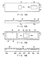
- Figs. 3A to 3D are plane views representing the electrode patterns and explaining the steps of manufacturing the device shown in Fig. 1.
- Figs. 4A to 4I are sectional views, explaining the steps of manufacturing the device shown in Fig. 1.
- Figs. 4A to 4D are sectional views taken along lines 4A-4A to 4D-4D which are shown in Figs. 3A to 3D, respectively.
- the component identical to those shown in Figs. 1 and 2 are denoted at the same reference numerals.
- the surface region of the P-type silicon substrate 10, which has resistivity of 25 ⁇ cm, is heated at about 1000°C and thermally oxidized, thus forming a silicon oxide film 30 having a thickness of about 1 ⁇ m.
- the silicon oxide film 30 is patterned by means of photoetching, thus forming windows 32 in the film 30. Antimony is diffused through these windows 32 into the P-type substrate 10, thereby forming N+-buried layers 341 to 343 in the substrate 10, the layers 341 to 343 having a sheet resistance of 20 ⁇ / ⁇ . Then, the silicon oxide film 30 is removed from the substrate 10.
- an N-type silicon epitaxial layer 12 containing phosphorus and having resistivity of about 5 ⁇ cm is grown to the thickness of about 5 ⁇ m, on the upper surface of the resultant structure. While the layer 12 is growing, the impurities diffuse into the layer 12 from the portions forming N+-buried layers 341, 342 and 343 between the substrate 10 and the epitaxial layer 12. Theses layers 341, 342 and 343 have impurity concentrations higher than that of the epitaxial layer 12.
- the surface of the epitaxial layer 12 is subjected to thermal oxidation at 1000°C, thereby forming a silicon oxide film (not shown) having a thickness of about 500 ⁇ and serving as a photoresist pad. Then a photoresist (not shown) is formed on the silicon oxide film, a portion of the photoresist is removed by photoetching, thus forming an opening. Phosphorus ions, for example, are injected through the opening into the epitaxial layer 12, thereby forming a collector region. The remaining photoresist is removed from the silicon oxide film. Next, a photoresist is formed on the silicon oxide film. The photoresist is photo-etched, thereby openings made in the photoresist.
- Boron ions for example, are injected through these openings into the epitaxial layer 12, thereby forming P-type wells and P-type isolation diffusion layers in the layer 12.
- the photoresist removed from the silicon oxide film.
- an undoped CVD oxide film (not shown) having a thickness of about 3000 ⁇ is formed on the upper surface of the resultant structure by means of a CVD method.
- the structure is subjected to cap annealing at about 1190°C, thereby forming, as is shown in Figs. 3C and 4C, an N+-collector region 42 reaching the N+-buried layer 342 two P-type wells 22 and 14, both reaching the P-type substrate 10, and also P+-type isolation layers 14 reaching the substrate 10.
- the P+-type isolation layers 14 isolate three islands 16, 18, and 20.
- the island 16 is formed of a part of the N-type epitaxial layer 12.
- the island 18 consists of a part of the N-type epitaxial layer 12 and N+-buried layer 341 which are electrically combined.
- the island 20 consists of a part of the N-type epitaxial layer 12 and N+-buried layer 342 which are electrically combined.
- a field oxide film 44 having a thickness of about 9000 ⁇ is formed by the known LOCOS method on the upper surface of the resultant structure.
- boron or phosphorus can be ion-injected into those surface portions of the structure on which the film 44 is to be formed, thereby to form channel stoppers 46 beneath the field oxide film 44.
- the exposed surface portion of he silicon epitaxial layer 12 are thermally oxidized at 950°C, forming a silicon oxide film 48 having a thickness of about 700 ⁇ .
- This oxide film 48 will be used as the gate insulating film of the MOSFETs and as the first gate insulating film of the CCD.
- Boron or phosphorus is ion-injected through the film 48 into the upper surface of the structure, thus performing channel-doping.
- a first polysilicon layer having a thickness of about 4000 ⁇ is formed by the CVD method on the upper surface of the structure. Phosphorus is diffused into the first polysilicon layer at 950°C, using phosphoryl chloride (POCl3) as impurity source.
- Phosphorus is diffused into the first polysilicon layer at 950°C, using phosphoryl chloride (POCl3) as impurity source.
- the first polysilicon layer is thereby rendered conductive, or made into an N+-type layer.
- a photoresist is coated on the first polysilicon layer, and the photoresist is photo-etched, thus forming a mask.
- RIE reactive ion etching
- the first polysilicon layer is patterned, forming the first transfer gate 501 of the CCD, the gate 502 of the P-channel MOSFET, and the gate 503 of the N-channel MOSFET.
- the silicon oxide film 48 is removed, by applying ammonium fluoride (NH4F), using the gates 501, 502 and 503 as mask.
- the exposed surface portions of the silicon layer are thermally oxidized at 950°C, forming a silicon oxide film 52 having a thickness of about 700 ⁇ .
- Boron ions for example, are injected the resultant structure, by using the first transfer gate 501 and a photoresist (not shown) as mask, thereby forming a barrier layer (not shown) of the CCD.
- boron ions were injected into selected portions of the silicon epitaxial layer 12 by means of photoetching, in order to form the base of the NPN bipolar transistor.
- the structure is annealed at 900°C, forming a P ⁇ -inner-base layer 54.
- a second polysilicon layer having a thickness of about 4000 ⁇ is formed on the upper surface of the resultant structure by, for example, the CVD method.
- Phosphorus diffused into the second polysilicon layer at 950°C, using phosphoryl chloride (POCl3) as impurity source, whereby the second polysilicon layer is made conductive, or becomes an N+-type layer.
- a photoresist is coated on the second polysilicon layer, and the photoresist is photoetched, thus forming a mask. Using this mask, reactive ion etching (RIE) is performed on the second polysilicon layer.
- RIE reactive ion etching
- arsenic ions for example, are injected into selected portions 58 of the silicon epitaxial layer 12 by means of photoetching, in order to form the N+-emitter of the NPN bipolar transistor, the N+-source/drain of the N-channel MOSFET, and the N+-source/drain of the CCD.
- the exposed surface portions of the silicon layer are thermally oxidized at 900°C, forming a silicon oxide film 60 on the second transfer gates 56.
- Boron ions for example, are injected to selected portions 62 of the silicon epitaxial layer 12 by means of photoetching, in order to form the P+-outer base of the NPN bipolar transistor, the P+-source/drain of the N-channel MOSFET and the N+-source/drain of the CCD.
- an interlayer insulator film 64 consisting of a silicon oxide film and a BPS (Boro-Phospho Silicate) glass film is formed on the resultant structure by means of the CVD method. More specifically, the silicon oxide film is formed on the upper surface of the structure, and then the BPS glass film is formed on the silicon oxide film.
- the silicate glass of the insulator film 64 is melted at about 950°C, thus performing not only glass-flowing but also phosphorous gettering. Simultaneously, the arsenic and boron, both ion-injected, are activated.
- the N+-source/drain layer 581 of the CCD As a result, there are formed the N+-source/drain layer 581 of the CCD, the N+-contact layer 582 of the island 16, the N+-source/drain layer 583 of the N-channel MOSFET, and the N+-emitter layer 584 of the NPN bipolar transistor.
- the P+-source/drain 621 of the P-channel MOSFET, and the P+-outer-base layer 622 of the NPN bipolar transistor are formed. Further, photoetching is applied, thereby forming contact holes 66 in the interlayer insulator film 64, exposing the N+ layers 581 to 584 and the P+ layers 621 and 622.
- a metal layer made of aluminum-silicon (1%) alloy and having a thickness of about 8000 ⁇ is formed on the upper surface of the resultant structure by means of, for example, spattering. Then, a photoresist is coated on the metal layer, and the photoresist is photo-etched, thus forming a mask. Using this mask, reactive ion etching (RIE) is performed on the metal layer. As a result, metal wirings 681 to 687 are formed.
- RIE reactive ion etching
- the three wirings 685, 686 and 687 are the emitter, base and collector wirings of the NPN bipolar transistor. Forming (?) process is performed at about 430°C, thus imparting desired characteristic to each active element.
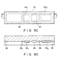
- FIGs. 5A to 5D are plane views representing the electrode patterns and explaining the steps of manufacturing the semiconductor device.
- Figs. 6A to 6E are sectional views, explaining the steps of manufacturing the second embodiment device.
- Figs. 6A to 6D are sectional views taken along lines 6A-6A to 6D-6D which are shown in Figs. 5A to 5D, respectively.
- the components shown in these figures, which are identical to those shown in Figs. 3A to 3D and Figs. 4A to 4I are denoted at the same reference numerals, and will not be described in detail.
- N+-buried layers 341 and 342, each having a sheet resistance of 20 ⁇ / ⁇ , are formed in a P-type silicon substrate 30 which has a sheet resistance of 25 ⁇ / ⁇ .
- a photoresist 35 is coated on the resultant structure.
- a selected portion of the photoresist 35 is removed by means of photoetching, thereby forming a window 36 in the photoresist 35.
- Boron ions are injected into the selected portions 38A and 40 of the substrate 30 through the windows 36. Thereafter, the remaining photoresist 35 is removed from the structure.
- an N-type silicon epitaxial layer 12 containing phosphorus and having resistivity of about 20 ⁇ cm is grown to the thickness of about 5 ⁇ m, on the upper surface of the resultant structure. While the layer 12 is growing, boron diffuses from the portions 38A and 40A of the substrate 30. As a result of this, N+-buried layers 341 and 342 and P+-buried layers 38 and 40 are formed between the substrate 30 and the epitaxial layer 12.
- the N+-buried layers 341 and 342 have impurity concentrations higher than the epitaxial layer 12, and the P+-buried layers 38 and 40 have impurity concentrations hither than that of the substrate 30.
- a N+-type collector region 42, P-type wells 22 and 24, and a P+-type isolation layer 14 are formed by the same method explained with reference to Figs. 3D and 4D.
- the N+-type collector region 42 extends from the upper surface of the epitaxial layer 12 to that of the N+-buried layer 342
- the P-type well 22 extends from the upper surface of the layer 12 to that of the P-type substrate 30.
- the P-type well 24 extends from the upper surface of the layer 12 to that of the P+-buried layer 40.
- the P+-type isolation layer 14 extends from the upper surface of the layer 12 to that of the P+-buried layer 38.
- the P+-type isolation layer 14 is divided into three islands 16, 18, and 20, in the same way as in Embodiment 1.
- an NPN bipolar transistor whose collector is the third island 20 are formed by the same method explained with reference to Figs. 4F to 4I.
- the semiconductor device according to the second embodiment of the invention which is illustrated in Fig. 6E.
- the device have the same advantages as have been described with reference to Figs. 1 and 2.
- this device is advantageous in that it is hardly latched up and operate with high reliability since the P+-buried layers 38 and 40, which are formed between the P-type substrate 30 and the P-type isolation diffusion layer 14 and has an impurity concentration higher than that of the diffusion layer 14.
Landscapes
- Engineering & Computer Science (AREA)
- Power Engineering (AREA)
- Physics & Mathematics (AREA)
- Condensed Matter Physics & Semiconductors (AREA)
- General Physics & Mathematics (AREA)
- Computer Hardware Design (AREA)
- Microelectronics & Electronic Packaging (AREA)
- Metal-Oxide And Bipolar Metal-Oxide Semiconductor Integrated Circuits (AREA)
- Solid State Image Pick-Up Elements (AREA)
- Element Separation (AREA)
Applications Claiming Priority (2)
| Application Number | Priority Date | Filing Date | Title |
|---|---|---|---|
| JP2009576A JPH07109860B2 (ja) | 1990-01-19 | 1990-01-19 | 電荷転送デバイスを含む半導体装置およびその製造方法 |
| JP9576/90 | 1990-01-19 |
Publications (2)
| Publication Number | Publication Date |
|---|---|
| EP0438167A1 true EP0438167A1 (fr) | 1991-07-24 |
| EP0438167B1 EP0438167B1 (fr) | 1996-03-20 |
Family
ID=11724141
Family Applications (1)
| Application Number | Title | Priority Date | Filing Date |
|---|---|---|---|
| EP91100577A Expired - Lifetime EP0438167B1 (fr) | 1990-01-19 | 1991-01-18 | Dispositif à semi-conducteur avec un dispositif à transfert de charge, MOSFETs et transistors bipolaires - tous formés dans un seul substrat semi-conducteur |
Country Status (5)
| Country | Link |
|---|---|
| US (1) | US5184203A (fr) |
| EP (1) | EP0438167B1 (fr) |
| JP (1) | JPH07109860B2 (fr) |
| KR (1) | KR940003378B1 (fr) |
| DE (1) | DE69117988T2 (fr) |
Cited By (3)
| Publication number | Priority date | Publication date | Assignee | Title |
|---|---|---|---|---|
| EP0603437A1 (fr) * | 1992-09-02 | 1994-06-29 | Motorola, Inc. | Dispositif à semi-conducteur comportant une capacité parasite réduite et méthode de fabrication |
| GB2561388A (en) * | 2017-04-13 | 2018-10-17 | Raytheon Systems Ltd | Silicon carbide integrated circuit |
| US10665703B2 (en) | 2017-04-13 | 2020-05-26 | Raytheon Systems Limited | Silicon carbide transistor |
Families Citing this family (10)
| Publication number | Priority date | Publication date | Assignee | Title |
|---|---|---|---|---|
| US6021172A (en) | 1994-01-28 | 2000-02-01 | California Institute Of Technology | Active pixel sensor having intra-pixel charge transfer with analog-to-digital converter |
| US6570617B2 (en) | 1994-01-28 | 2003-05-27 | California Institute Of Technology | CMOS active pixel sensor type imaging system on a chip |
| US5471515A (en) * | 1994-01-28 | 1995-11-28 | California Institute Of Technology | Active pixel sensor with intra-pixel charge transfer |
| USRE42918E1 (en) | 1994-01-28 | 2011-11-15 | California Institute Of Technology | Single substrate camera device with CMOS image sensor |
| JP3547811B2 (ja) * | 1994-10-13 | 2004-07-28 | 株式会社ルネサステクノロジ | バイポーラトランジスタを有する半導体装置およびその製造方法 |
| JPH08289180A (ja) | 1995-02-14 | 1996-11-01 | Nikon Corp | 電子スチルカメラ |
| US5880515A (en) | 1996-09-30 | 1999-03-09 | Lsi Logic Corporation | Circuit isolation utilizing MeV implantation |
| US6909150B2 (en) * | 2001-07-23 | 2005-06-21 | Agere Systems Inc. | Mixed signal integrated circuit with improved isolation |
| JP4510414B2 (ja) * | 2003-09-12 | 2010-07-21 | キヤノン株式会社 | 光電変換装置 |
| JP2007067012A (ja) * | 2005-08-29 | 2007-03-15 | Matsushita Electric Ind Co Ltd | 半導体装置 |
Citations (4)
| Publication number | Priority date | Publication date | Assignee | Title |
|---|---|---|---|---|
| US4646124A (en) * | 1984-07-30 | 1987-02-24 | Sprague Electric Company | Level shifting BIMOS integrated circuit |
| EP0242748A1 (fr) * | 1986-04-17 | 1987-10-28 | Honeywell Inc. | Circuit d'entrée bipolaire/MOS pour détecteurs photovoltaiques |
| EP0245515A1 (fr) * | 1985-11-20 | 1987-11-19 | Hitachi, Ltd. | Dispositif a semi-conducteurs |
| EP0392536A2 (fr) * | 1989-04-13 | 1990-10-17 | Kabushiki Kaisha Toshiba | Dispositif semi-conducteur comprenant un CCD et ses transistors bipolaires périphériques et son procédé de fabrication |
Family Cites Families (5)
| Publication number | Priority date | Publication date | Assignee | Title |
|---|---|---|---|---|
| US4152715A (en) * | 1977-11-28 | 1979-05-01 | The United States Of America As Represented By The Secretary Of The Army | Silicon base CCD-bipolar transistor compatible methods and products |
| US4253168A (en) * | 1978-10-23 | 1981-02-24 | Westinghouse Electric Corp. | CCD Signal processor |
| CA1151295A (fr) * | 1979-07-31 | 1983-08-02 | Alan Aitken | Dispositifs mos a deux resistivites et methode de fabrication |
| JPS60141157U (ja) * | 1984-02-25 | 1985-09-18 | ソニー株式会社 | 電荷結合素子 |
| JPH01194348A (ja) * | 1988-01-28 | 1989-08-04 | Nec Corp | 半導体装置 |
-
1990
- 1990-01-19 JP JP2009576A patent/JPH07109860B2/ja not_active Expired - Fee Related
-
1991
- 1991-01-16 US US07/641,920 patent/US5184203A/en not_active Expired - Lifetime
- 1991-01-17 KR KR1019910000692A patent/KR940003378B1/ko not_active IP Right Cessation
- 1991-01-18 EP EP91100577A patent/EP0438167B1/fr not_active Expired - Lifetime
- 1991-01-18 DE DE69117988T patent/DE69117988T2/de not_active Expired - Fee Related
Patent Citations (4)
| Publication number | Priority date | Publication date | Assignee | Title |
|---|---|---|---|---|
| US4646124A (en) * | 1984-07-30 | 1987-02-24 | Sprague Electric Company | Level shifting BIMOS integrated circuit |
| EP0245515A1 (fr) * | 1985-11-20 | 1987-11-19 | Hitachi, Ltd. | Dispositif a semi-conducteurs |
| EP0242748A1 (fr) * | 1986-04-17 | 1987-10-28 | Honeywell Inc. | Circuit d'entrée bipolaire/MOS pour détecteurs photovoltaiques |
| EP0392536A2 (fr) * | 1989-04-13 | 1990-10-17 | Kabushiki Kaisha Toshiba | Dispositif semi-conducteur comprenant un CCD et ses transistors bipolaires périphériques et son procédé de fabrication |
Non-Patent Citations (1)
| Title |
|---|
| ELECTRONICS 28 October 1976, pages 8E,10E; "One process adapts CCD devices to MOS, bipolar peripheral circuits" * |
Cited By (7)
| Publication number | Priority date | Publication date | Assignee | Title |
|---|---|---|---|---|
| EP0603437A1 (fr) * | 1992-09-02 | 1994-06-29 | Motorola, Inc. | Dispositif à semi-conducteur comportant une capacité parasite réduite et méthode de fabrication |
| SG85053A1 (en) * | 1992-09-02 | 2001-12-19 | Motorola Inc | Semiconductor device and method of formation |
| GB2561388A (en) * | 2017-04-13 | 2018-10-17 | Raytheon Systems Ltd | Silicon carbide integrated circuit |
| GB2561388B (en) * | 2017-04-13 | 2019-11-06 | Raytheon Systems Ltd | Silicon carbide integrated circuit |
| US10665703B2 (en) | 2017-04-13 | 2020-05-26 | Raytheon Systems Limited | Silicon carbide transistor |
| US11450568B2 (en) | 2017-04-13 | 2022-09-20 | Raytheon Systems Limited | Silicon carbide integrated circuit |
| US11626325B2 (en) | 2017-04-13 | 2023-04-11 | Raytheon Systems Limited | Method of making a silicon carbide integrated circuit |
Also Published As
| Publication number | Publication date |
|---|---|
| DE69117988T2 (de) | 1996-09-05 |
| EP0438167B1 (fr) | 1996-03-20 |
| JPH03214665A (ja) | 1991-09-19 |
| JPH07109860B2 (ja) | 1995-11-22 |
| KR940003378B1 (ko) | 1994-04-21 |
| DE69117988D1 (de) | 1996-04-25 |
| US5184203A (en) | 1993-02-02 |
Similar Documents
| Publication | Publication Date | Title |
|---|---|---|
| EP0110313B1 (fr) | Dispositif de circuit intégré semi-conducteur et procédé de fabrication | |
| US6194763B1 (en) | Semiconductor device having SOI-MOSFET | |
| EP0225821B1 (fr) | Dispositif semi-conducteur à structure silicium sur isolant | |
| US5028975A (en) | Semiconductor devices and a process for producing the same | |
| EP0052450A1 (fr) | Procédé de fabrication d'un dispositif semiconducteur comprenant des électrodes en semiconducteur polycristallin et métal | |
| US4845532A (en) | Semiconductor devices | |
| US5591662A (en) | Method of manufacturing a power integrated circuit (PIC) structure | |
| EP0438167B1 (fr) | Dispositif à semi-conducteur avec un dispositif à transfert de charge, MOSFETs et transistors bipolaires - tous formés dans un seul substrat semi-conducteur | |
| US5191401A (en) | MOS transistor with high breakdown voltage | |
| US5220190A (en) | Device having a charge transfer device, MOSFETs, and bipolar transistors--al | |
| US4893164A (en) | Complementary semiconductor device having high switching speed and latchup-free capability | |
| US4662057A (en) | Method of manufacturing a semiconductor integrated circuit device | |
| US5260228A (en) | Method of making a semiconductor device having a charge transfer device, MOSFETs, and bipolar transistors | |
| US5043788A (en) | Semiconductor device with functional portions having different operating voltages on one semiconductor substrate | |
| US5286986A (en) | Semiconductor device having CCD and its peripheral bipolar transistors | |
| KR930002296B1 (ko) | 전하전송 디바이스를 포함한 반도체장치 및 그 제조방법 | |
| US5198880A (en) | Semiconductor integrated circuit and method of making the same | |
| US5122855A (en) | Semiconductor device with latch-up prevention structure | |
| KR930008022B1 (ko) | 반도체장치 | |
| EP0428067A2 (fr) | Circuit intégré à semi-conducteur et son procédé de fabrication | |
| EP0404180B1 (fr) | Circuit intégré à semi-conducteur et procédé pour sa fabrication | |
| EP0427253A2 (fr) | Dispositif de circuit intégré semi-conducteur comprenant des transistors bipolaires, des TEC de type MOS et CCD | |
| JP2680846B2 (ja) | 半導体記憶装置 | |
| JPH0745731A (ja) | 半導体集積回路装置とその製造方法 | |
| KR19990056720A (ko) | 반도체 전력소자 및 그의 제조방법 |
Legal Events
| Date | Code | Title | Description |
|---|---|---|---|
| PUAI | Public reference made under article 153(3) epc to a published international application that has entered the european phase |
Free format text: ORIGINAL CODE: 0009012 |
|
| 17P | Request for examination filed |
Effective date: 19910118 |
|
| AK | Designated contracting states |
Kind code of ref document: A1 Designated state(s): DE FR GB |
|
| 17Q | First examination report despatched |
Effective date: 19940427 |
|
| GRAH | Despatch of communication of intention to grant a patent |
Free format text: ORIGINAL CODE: EPIDOS IGRA |
|
| GRAA | (expected) grant |
Free format text: ORIGINAL CODE: 0009210 |
|
| AK | Designated contracting states |
Kind code of ref document: B1 Designated state(s): DE FR GB |
|
| REF | Corresponds to: |
Ref document number: 69117988 Country of ref document: DE Date of ref document: 19960425 |
|
| ET | Fr: translation filed | ||
| PLBE | No opposition filed within time limit |
Free format text: ORIGINAL CODE: 0009261 |
|
| STAA | Information on the status of an ep patent application or granted ep patent |
Free format text: STATUS: NO OPPOSITION FILED WITHIN TIME LIMIT |
|
| 26N | No opposition filed | ||
| PGFP | Annual fee paid to national office [announced via postgrant information from national office to epo] |
Ref country code: GB Payment date: 19980109 Year of fee payment: 8 Ref country code: FR Payment date: 19980109 Year of fee payment: 8 |
|
| PG25 | Lapsed in a contracting state [announced via postgrant information from national office to epo] |
Ref country code: GB Free format text: LAPSE BECAUSE OF NON-PAYMENT OF DUE FEES Effective date: 19990118 |
|
| GBPC | Gb: european patent ceased through non-payment of renewal fee |
Effective date: 19990118 |
|
| PG25 | Lapsed in a contracting state [announced via postgrant information from national office to epo] |
Ref country code: FR Free format text: LAPSE BECAUSE OF NON-PAYMENT OF DUE FEES Effective date: 19990930 |
|
| REG | Reference to a national code |
Ref country code: FR Ref legal event code: ST |
|
| PGFP | Annual fee paid to national office [announced via postgrant information from national office to epo] |
Ref country code: DE Payment date: 20060112 Year of fee payment: 16 |
|
| PG25 | Lapsed in a contracting state [announced via postgrant information from national office to epo] |
Ref country code: DE Free format text: LAPSE BECAUSE OF NON-PAYMENT OF DUE FEES Effective date: 20070801 |