EP0436823A1 - Signalpegelwandler - Google Patents
Signalpegelwandler Download PDFInfo
- Publication number
- EP0436823A1 EP0436823A1 EP90122762A EP90122762A EP0436823A1 EP 0436823 A1 EP0436823 A1 EP 0436823A1 EP 90122762 A EP90122762 A EP 90122762A EP 90122762 A EP90122762 A EP 90122762A EP 0436823 A1 EP0436823 A1 EP 0436823A1
- Authority
- EP
- European Patent Office
- Prior art keywords
- transistor
- signal level
- level converter
- cml
- cmos
- Prior art date
- Legal status (The legal status is an assumption and is not a legal conclusion. Google has not performed a legal analysis and makes no representation as to the accuracy of the status listed.)
- Withdrawn
Links
- 230000005669 field effect Effects 0.000 claims abstract description 22
- 230000000295 complement effect Effects 0.000 claims description 8
- 238000010586 diagram Methods 0.000 description 8
- 230000004913 activation Effects 0.000 description 2
- 230000015572 biosynthetic process Effects 0.000 description 1
- 230000000903 blocking effect Effects 0.000 description 1
- 238000006243 chemical reaction Methods 0.000 description 1
- 238000011161 development Methods 0.000 description 1
- 230000018109 developmental process Effects 0.000 description 1
- 230000002349 favourable effect Effects 0.000 description 1
Images

Classifications
-
- H—ELECTRICITY
- H03—ELECTRONIC CIRCUITRY
- H03M—CODING; DECODING; CODE CONVERSION IN GENERAL
- H03M7/00—Conversion of a code where information is represented by a given sequence or number of digits to a code where the same, similar or subset of information is represented by a different sequence or number of digits
- H03M7/14—Conversion to or from non-weighted codes
- H03M7/20—Conversion to or from n-out-of-m codes
- H03M7/22—Conversion to or from n-out-of-m codes to or from one-out-of-m codes
-
- H—ELECTRICITY
- H03—ELECTRONIC CIRCUITRY
- H03K—PULSE TECHNIQUE
- H03K17/00—Electronic switching or gating, i.e. not by contact-making and –breaking
- H03K17/51—Electronic switching or gating, i.e. not by contact-making and –breaking characterised by the components used
- H03K17/56—Electronic switching or gating, i.e. not by contact-making and –breaking characterised by the components used by the use, as active elements, of semiconductor devices
- H03K17/60—Electronic switching or gating, i.e. not by contact-making and –breaking characterised by the components used by the use, as active elements, of semiconductor devices the devices being bipolar transistors
- H03K17/62—Switching arrangements with several input- output-terminals, e.g. multiplexers, distributors
- H03K17/6257—Switching arrangements with several input- output-terminals, e.g. multiplexers, distributors with several inputs only combined with selecting means
- H03K17/6264—Switching arrangements with several input- output-terminals, e.g. multiplexers, distributors with several inputs only combined with selecting means using current steering means
-
- H—ELECTRICITY
- H03—ELECTRONIC CIRCUITRY
- H03K—PULSE TECHNIQUE
- H03K17/00—Electronic switching or gating, i.e. not by contact-making and –breaking
- H03K17/51—Electronic switching or gating, i.e. not by contact-making and –breaking characterised by the components used
- H03K17/56—Electronic switching or gating, i.e. not by contact-making and –breaking characterised by the components used by the use, as active elements, of semiconductor devices
- H03K17/687—Electronic switching or gating, i.e. not by contact-making and –breaking characterised by the components used by the use, as active elements, of semiconductor devices the devices being field-effect transistors
- H03K17/693—Switching arrangements with several input- or output-terminals, e.g. multiplexers, distributors
-
- H—ELECTRICITY
- H03—ELECTRONIC CIRCUITRY
- H03K—PULSE TECHNIQUE
- H03K19/00—Logic circuits, i.e. having at least two inputs acting on one output; Inverting circuits
- H03K19/0175—Coupling arrangements; Interface arrangements
- H03K19/017509—Interface arrangements
- H03K19/017518—Interface arrangements using a combination of bipolar and field effect transistors [BIFET]
- H03K19/017527—Interface arrangements using a combination of bipolar and field effect transistors [BIFET] with at least one differential stage
-
- H—ELECTRICITY
- H03—ELECTRONIC CIRCUITRY
- H03K—PULSE TECHNIQUE
- H03K19/00—Logic circuits, i.e. having at least two inputs acting on one output; Inverting circuits
- H03K19/0175—Coupling arrangements; Interface arrangements
- H03K19/0185—Coupling arrangements; Interface arrangements using field effect transistors only
- H03K19/018507—Interface arrangements
- H03K19/018514—Interface arrangements with at least one differential stage
Definitions
- the invention relates to a signal level converter according to the preamble of patent claim 1.
- Such signal level converters are generally provided to identify the binary value represented by a CMOS logic signal level in accordance with CMOS standards and to generate a corresponding signal level provided in accordance with the power switch logic (CML) or emitter-coupled logic (ECL) to represent this binary value .
- CML power switch logic
- ECL emitter-coupled logic
- the digital H level is at the more positive value of the two supply voltage potential and the digital L- Level at a voltage value that is only about 0.5 volts more negative.
- the digital H level is approximately 0.9 volts and the digital L level is approximately 1.7 volts more negative than the more positive value of the two supply voltage potentials.
- a signal level converter for converting CMOS logic input signal levels to CML or ECL output signal levels must have an input signal level swing of 5 volts to an output signal level swing of 0.5 volts for CML and Implement ECL - taking into account the respective signal-to-noise ratios.
- CMOS-CML / ECL level converter A known signal level converter for converting CMOS logic input signal levels to CML or ECL output signal levels, hereinafter referred to as CMOS-CML / ECL level converter, consists of a slightly modified switching stage of the CML or ECL circuit technology.
- Such a switching stage of the CML or ECL circuit technology is formed from a constant current-fed differential amplifier with a first and a second amplifier branch, each of which has a control or reference transistor designed as an NPN transistor.
- the emitter electrodes of the two NPN transistors are connected to one another and connected to the constant current source.
- the base electrode of the control transistor serves as a switching stage input, that of the reference transistor is acted upon by a constant reference voltage potential which defines the switching threshold of the switching stage and thus has the voltage value which must be exceeded or fallen below at the switching stage input in order for the switching stage to switch.
- the collector electrodes of both NPN transistors provide complementary switching stage outputs and are each connected via a load resistor to the more positive of the two supply voltage potentials, which is also called the level reference potential, since it represents a digital CML and CMOS-H level.
- such a switching stage is supplied with a reference voltage potential which has a value in the middle between the two voltage values for the digital levels of the CMOS circuit technology (at 0 volts for the digital H level and -5 volt for the digital L level, the reference voltage potential has the value of -2.5 volt).
- the load resistance of the control transistor must be omitted, since the switching stage input serves as a signal level converter input and the control transistor already has a very low collector-emitter voltage in the conductive state, so that the saturation of the control transistor can only be reliably prevented without a load resistor. As is known, saturation of the control transistor leads to an undesirable increase in the signal propagation time.
- the known signal level converter therefore does not provide any complementary signal level converter outputs.
- a series connection of several control transistors in the first amplifier branch to form a logical AND operation cannot be realized for the same reason.
- a parallel connection of several control transistors to form a logical OR logic circuit is also not feasible, since the maximum base-emitter voltage of a blocking control transistor is exceeded with input signal levels in phase opposition.
- the object of the present invention is therefore to develop a signal level converter according to the preamble of claim 1 so that the further developed signal level converter can be modified with little effort, so that in addition to level conversion, logical functions can also be implemented.
- a control transistor designed as a field-effect transistor offers the essential advantage over a bipolar transistor with regard to the subject matter of the invention that its drain-source voltage may become as low as desired without a saturation state being established, as in the case of a bipolar transistor.
- the reference voltage potential does not necessarily have to have a value lying in the middle between the two voltage values for the digital CMOS levels.
- the effort for the formation of the reference voltage potential can thus be reduced, especially since the reference voltage potential formed for switching stages of the CML or ECL circuit technology for determining the switching threshold can also be used as the reference voltage potential.
- control transistor is designed as a P-channel field effect transistor, the switching threshold of the signal level converter is not influenced by the level of the reference voltage potential.
- a signal level converter designed according to the invention can be expanded with little circuitry means for realizing logic functions, complex logic switching stages for forming these functions can be saved. This increases the gate density on an integrated circuit and reduces the signal delay and the power loss.
- the known signal level converter is formed from a switching stage of the CML circuit technology and consists of a differential amplifier arrangement serving as a current switch with a first and a second amplifier branch fed from a common constant current source.
- Two supply voltage potentials VEE, VCC with a voltage value of -5Volt or 0V are provided for the voltage supply of the switching stage.
- a current source transistor ST in the form of an NPN transistor, is used as the constant current source, the emitter electrode of which is connected via an emitter resistor to the more negative of the two supply voltage potentials VEE.
- a constant voltage VSI is supplied to the base electrode of the current source transistor Q, the voltage value of which determines the collector current of the current source transistor Q as a function of the emitter resistance.
- the first amplifier branch leads from the collector electrode of the current source transistor Q via the emitter-collector path of a control transistor ST designed as an NPN transistor to more positive of the two supply voltage potentials VCC (0 volt), which also serves as a level reference potential for CMOS-H level and CML-H level.
- the base electrode of the control transistor ST serves as a signal level converter input E-CMOS for CMOS input signal levels, which are represented by the voltage values of the two supply voltage potentials VCC, VEE.
- the second amplifier branch leads from the collector electrode of the current source transistor Q via the emitter-collector path of a reference transistor RT designed as an NPN transistor and via a load resistor R connected to its collector electrode to the more positive of the two supply voltage potentials VCC.
- the collector electrode of the emitter follower is connected to the more positive of the two supply voltage potentials VCC, its emitter electrode serves as a signal level converter output A-ECL for ECL output signal levels.
- a reference voltage potential is applied to the base electrode of the reference transistor RT, which potential is generated with the aid of a bridged CMOS inverter.
- the bridged CMOS inverter (shown in the FIG by means of a broken line from the signal level converter) consists of a series connection of a P-channel and an N-channel MOS field-effect transistor, the drain and gate electrodes of which are connected to one another and a connecting line to the base of the reference transistor Have RT.
- CMOS inverter With the bridged CMOS inverter, a voltage value (i.e. - 2.5 volts) lying in the middle between the two supply voltage potentials VCC, VEE is generated, so that the switching threshold of the signal level converter is exactly in the middle between the two voltage values for digital CMOS levels lies.
- the current generated by the constant current source flows e.g. 1 milliampere completely through the first amplifier branch, the voltage value of the CMOS input signal is at least 100 millivolts more negative, then the current flows completely through the second amplifier branch.
- a CMOS-H level at the signal level converter input E-CMOS therefore does not lead to a voltage drop across the load resistor R in the second amplifier branch.
- a CML-H level is therefore available at the signal level converter output A-CML.
- the reference transistor RT With a CMOS-L level at the signal converter input E-CMOS, the reference transistor RT is conductive and at the load resistor R, which e.g. has an ohmic value of approximately 500 ohms, a voltage drop of approximately 0.5 volts is formed, which corresponds to the amount according to the CML-L level.
- a saturation of the control transistor ST with an applied CMOS-H level at the signal level converter input E-CMOS cannot occur since the collector-emitter voltage cannot become less than 0.7 volts (corresponds to the base-emitter voltage) due to a lack of load resistance in the first amplifier branch and is thus far above the saturation voltage of approx. 0.2 volts.
- FIG. 2 shows a circuit diagram for a CMOS-ECL level converter developed according to the invention, which, like the known signal level converter according to FIG. 1, consists of a differential amplifier arrangement serving as a current switch, with a first and a second of a common one Constant current source fed amplifier branch is formed.
- the constant current source is identical to that of the known signal level converter and is shown in the form of a current source symbol to simplify the drawing.
- the first amplifier branch has three control transistors ST1, ST2, ST3 designed as self-blocking P-channel MOS field-effect transistors. Since these field-effect transistors, hereinafter referred to as PMOS-FETs, are symmetrical with regard to their drain-source electrode arrangement, the electrode lying at a more positive voltage potential is always the source electrode.
- the first amplifier branch is composed as follows.
- the drain electrodes of a second and a third, control transistor ST2, ST3 are connected to the current source SQ.
- the interconnected source electrodes of the second and third control transistor ST2, ST3 are led to the drain electrode of a first control transistor ST1, the source electrode of which has a tap serving as a signal level converter output A-CML / and via a further load resistor with the more positive of the two Supply voltage potential VCC is connected.
- the gate electrodes of the three control transistors ST1, ST2, ST3 serve as signal level converter inputs E1-CMOS, E2-CMOS, E3-CMOS for CMOS input signal levels.
- the second amplifier branch consists of a reference transistor RT designed as an NPN transistor, which is connected with its emitter electrode to the current source SQ and with its collector electrode via a load resistor R to the more positive of the two supply voltage potentials VCC. There is also a tap on the collector electrode of the reference transistor RT which serves as a logically complementary signal level converter output A-CML for CML signal levels.
- the base electrode of the reference transistor RT is supplied with a reference voltage potential of approximately - 0.25 volts, that is also required to determine the switching threshold for CML switching stages and is usually already available.
- a CMOS-H level at the gate electrode of a control transistor achieves a gate-source voltage of 0 volts, the control transistor in question is therefore extremely high-resistance.
- the control transistor in question With a CMOS-L level at the gate electrode, the control transistor in question is turned on. If the current (e.g. 1 milliampere) flows from the constant current source SQ through the first amplifier branch, a voltage drop of 0.5 volt forms at the load resistor of the first amplifier branch, which corresponds to a CML-L level.
- control transistors ST1, ST2, ST3 are dimensioned with regard to their threshold point so that the switching threshold of the signal level converter lies approximately in the middle between the two voltage values for the digital CMOS signal levels.
- FIG. 3 shows a circuit diagram for a CMOS-CML signal level converter which is supplemented in accordance with the invention for performing logic functions and which has an activation input for supplying a CML signal level.
- This signal level converter also consists of a first and a second amplifier branch fed by a common constant current source SQ.
- the first amplifier branch has two control transistors ST1, ST2 which are connected in parallel and are designed as PMOS-FETs and which are connected with their drain electrodes to the constant current source SQ and with their source electrodes to the more positive of the two supply voltage potentials VCC are.
- An input transistor ET designed as an NPN transistor is connected with its emitter electrode to the constant current source SQ and with its collector electrode to the more positive of the two supply voltage potentials VCC and is thus connected in parallel with the first amplifier branch.
- the base electrode of the input transistor serves as the enable input E-CML of the signal level converter and is supplied with CML signal levels.
- the gate electrodes of the two control transistors ST1, ST2 serve as signal level converter inputs E1-CMOS and E2-CMOS for CMOS signal levels.
- the second amplifier branch is identical to that of the signal level converter according to FIG. 2.
- the current of the constant current source only flows through the second amplifier branch (i.e. a CML-L level is set at the signal level converter output A-CML) if E1-CMOS, E2 at both signal level converter inputs -CMOS a CMOS H level is present.
- the signal level converter thus carries out a logical not-or operation.
- FIG. 4 shows a circuit diagram for a CMOS-CML signal level converter which is supplemented with a one of three decoding logic in accordance with the invention.
- This signal level converter also has a first and a second amplifier branch fed from a common constant current source SQ.
- a control transistor ST designed as a PMOS-FET is arranged in the first amplifier branch and is connected with its drain electrode to the constant current source SQ and with its source electrode via a load resistor to the more positive of the two supply voltage potentials VCC.
- a tap connected to the source electrode forms a signal level converter output A1-CML for CML signal levels.
- the gate electrode of the control transistor ST serves as a signal level converter input E-CMOS for CMOS signal levels.
- the second amplifier branch is identical to that of the signal level converter according to FIG. 2 or FIG. 3.
- a third amplifier branch is formed by a bridge transistor BT designed as an NPN transistor, the emitter electrode of which is connected to the constant current source SQ and the collector electrode of which is connected via a third load resistor R3 to the more positive of the two supply voltage potentials VCC.
- a tap on the collector electrode of the bridge transistor BT serves as the third signal level converter output A3-CML for CML output signal levels.
- the base of the bridge transistor BT is connected to a further current source SQ1, which is connected to the more negative of the two supply voltage potentials, and via the emitter-collector path of an input transistor ET, which is designed as an NPN transistor and works as an emitter follower, to the more positive one of the two supply voltage potentials VCC.
- the base electrode of the input transistor ET is at CML input signal levels acted upon and serves as a selection input for the 1 out of three of the decoding logic formed with the signal level converter.
- the input transistor ET in conjunction with the further current source SQ1 serves to prevent the base voltage at the bridge transistor BT in the conductive state, that is, when the CML-H level is present, from becoming so positive that the bridge transistor BT saturates due to the voltage drop across the third load resistor R3 goes.
- a value table is given below, which, depending on the digital input signal level combinations at the selection input E-CML and at the signal level converter input E-CMOS, is connected to the signal level converter outputs A1-CML, A2-CML, A3- CML specifies the digital output signal level.
- FIG. 5 shows a circuit diagram for a CMOS-CML signal level converter designed according to the invention to form a signal selection logic.
- This signal level converter consists of a base differential amplifier with a first and a second base amplifier fed by a common constant current source, in each of which a downstream differential amplifier is arranged.
- the first base amplifier branch there is a base control transistor BST designed as a PMOS-FET, which is connected with its drain electrode to the constant current source SQ and is connected at its source electrode to the two amplifier branches of the downstream differential amplifier arranged in the first base amplifier branch.
- the second base amplifier branch has a base reference transistor BRT designed as an NPN transistor, the emitter electrode of which is connected to the constant current source SQ and the collector electrode of which is connected to the two amplifier branches of the downstream differential amplifier arranged in the second base amplifier branch.
- the downstream differential amplifiers are constructed identically and each consist of a first and a second amplifier branch with a control transistor ST1 designed as a PMOS-FET; ST2 in the first amplifier branch and a reference transistor RT1 in the form of an NPN transistor; RT2 in the second amplifier branch.
- the drain electrode of the control transistor ST1 is connected to the emitter electrode of the reference transistor RT1 and is connected to the source electrode of the base control transistor BST.
- the drain electrode of the control transistor ST2 is connected to the emitter electrode of the reference transistor RT2 and connected to the collector electrode of the base reference transistor BRT in the downstream differential amplifier of the second base amplifier branch.
- control transistors ST1, ST2 are connected to the more positive of the two supply voltage potentials VCC.
- the reference transistors RT1, RT2 of the two differential amplifiers connected downstream are connected to one another at their collector electrodes and are also connected via a load resistor R to the more positive of the two supply voltage potentials VCC.
- a tap on the collector electrode of the reference transistors RT1, RT2 and thus on the load resistor R serves as a signal level converter output A-CML for CML signal levels.
- the base electrodes of the two reference transistors RT1, RT2 in the downstream differential amplifiers are connected to one another and are connected to a first reference voltage potential VSVX applied, the voltage value of which is approximately between the two voltage values for the digital CML levels at approximately - 0.25 volts.
- a second reference voltage potential VSVY is led to the base electrode of the base reference transistor BRT, the voltage value of which is more negative than that of the first reference voltage potential VSVX by at least the saturation voltage of the base reference transistor BRT, that is to say is approximately - 1.0 volt.
- the gate electrode of the base control transistor BST serves as a selection input E-CMOS for CMOS signal levels and the gate electrodes of the control transistors ST1, ST2 belonging to the downstream differential amplifiers serve as signal level converter inputs E1-CMOS, E2-CMOS for CMOS signal levels.
- FIG. 6 shows a circuit diagram for a CMOS-CML signal level converter provided with a reference transistor designed as a field effect transistor.
- This signal level converter also consists of a first and a second amplifier branch fed by a common constant current source.
- the first amplifier branch has two control transistors ST1, ST2 connected in series and designed as PMOS fets, the gate electrodes of which serve as signal level converter inputs E1-CMOS, E2-CMOS for CMOS signal levels.
- a reference transistor RT designed as a self-blocking N-channel MOS-Fet, hereinafter abbreviated N-MOS-Fet, is arranged, whose source electrode is connected to the constant current source SQ and its drain electrode is connected via a load resistor R to the more positive one both supply voltage potentials VCC is connected.
- a tap on the drain electrode and thus on the load resistor R serves as a signal level converter output A-CML for CML signal levels.
- the gate electrode of the reference transistor RT is connected to the more positive of the two supply voltage potentials VCC.
- the current of the constant current source SQ only flows through the first amplifier branch when an L level is present at both signal level converter inputs E1-CMOS, E2-CMOS. Because then the two control transistors ST1, ST2 have a low resistance and at the same time the gate-source voltage at the reference transistor RT has dropped below the threshold point of the reference transistor RT, as a result of which the reference transistor RT becomes high-resistance.
- the first amplifier branch has a high resistance and the gate-source voltage at the reference transistor RT is higher the threshold of the reference transistor RT.
- the signal level converter output A-CML there is a voltage value of - 0.5 volts corresponding to a CML-L level.
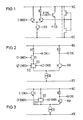
- FIG. 7 shows a circuit diagram for a CMOS-CML signal level converter provided with complementarily assigned reference transistors in accordance with the invention.
- each control transistor ST1, ST2 in the first amplifier branch is uniquely assigned a reference transistor RT designed as an N-MOS-FET in the second amplifier branch.
- the switching network formed by the reference transistors RT1, RT2 is complementary to that of the control transistors ST1, ST2.
- the control transistors ST1, ST2 are connected in series to form an AND link, the reference transistors RT1, RT2 are therefore connected in parallel to form the complementary switching network, that is to say for an OR link.
- control transistors ST1, ST2 serve as signal level converter inputs E1-CMOS, E2-CMOS for CMOS signal levels, and each reference transistor RT1, RT2 has its gate electrode connected to that of the control transistor ST1, ST2 assigned to it.
- the current of the constant current source SQ only flows through the first amplifier branch if there are L levels at the two signal level converter inputs E1-CMOS, E2-CMOS, because then the gate-source voltage at both reference transistors RT1, RT2 has become 0, with which these then become high impedance.
- the first amplifier branch is high-resistance and the current flows completely through the second amplifier branch, since at least one of the reference transistors RT1, RT2 due to a high Gate-source voltage becomes low.
- the signal level converter according to FIG. 7 has a steeper transfer curve which is therefore more favorable for the switching behavior.
- FIG. 8 shows a circuit diagram for a CMOS-CML signal level converter provided with a reference transistor designed as a field effect transistor.
- the structure of this signal level converter is similar to the signal level converter according to FIG. 6.
- a load resistor R1 is provided in the first amplifier branch which connects the series connection of the control transistors ST1, ST2 and thus the source electrode of the control transistor ST1 facing away from the constant current source SQ to the more positive one of the two supply voltage potentials VCC.
- this signal level converter lies approximately between that of the signal level converter according to FIG. 6 and that according to FIG. 7.
- control transistors are designed as normally-off P-channel MOS field-effect transistors
- control transistors can e.g. also be designed as a self-conducting N-channel MOS field-effect transistors.
- each signal level converter output A-CML for CML signal levels can be followed by an emitter follower.
Landscapes
- Engineering & Computer Science (AREA)
- Computer Hardware Design (AREA)
- Physics & Mathematics (AREA)
- Computing Systems (AREA)
- General Engineering & Computer Science (AREA)
- Mathematical Physics (AREA)
- Theoretical Computer Science (AREA)
- Logic Circuits (AREA)
Applications Claiming Priority (2)
| Application Number | Priority Date | Filing Date | Title |
|---|---|---|---|
| DE19904000780 DE4000780C1 (enExample) | 1990-01-12 | 1990-01-12 | |
| DE4000780 | 1990-01-12 |
Publications (1)
| Publication Number | Publication Date |
|---|---|
| EP0436823A1 true EP0436823A1 (de) | 1991-07-17 |
Family
ID=6397987
Family Applications (1)
| Application Number | Title | Priority Date | Filing Date |
|---|---|---|---|
| EP90122762A Withdrawn EP0436823A1 (de) | 1990-01-12 | 1990-11-28 | Signalpegelwandler |
Country Status (4)
| Country | Link |
|---|---|
| EP (1) | EP0436823A1 (enExample) |
| JP (1) | JPH04212518A (enExample) |
| DE (1) | DE4000780C1 (enExample) |
| IE (1) | IE910093A1 (enExample) |
Cited By (7)
| Publication number | Priority date | Publication date | Assignee | Title |
|---|---|---|---|---|
| DE4227282C1 (de) * | 1992-08-18 | 1993-11-25 | Siemens Ag | Digitaler Stromschalter |
| WO1996031006A1 (fr) * | 1995-03-29 | 1996-10-03 | Matra Mhs | Dispositif d'interfaçage de signaux logiques du niveau ecl au niveau cmos |
| EP0785629A1 (en) * | 1996-01-17 | 1997-07-23 | Nec Corporation | Level conversion circuit having differential circuit employing MOSFET |
| EP0722221A3 (en) * | 1995-01-13 | 1998-02-11 | Nec Corporation | Current switching circuit operable at high speed without externally supplied reference bias |
| GB2335556A (en) * | 1998-03-18 | 1999-09-22 | Ericsson Telefon Ab L M | BiMOS switched current source for a DAC or for a PLL charge pump |
| EP0973262A3 (en) * | 1998-07-13 | 2000-10-11 | Texas Instruments Incorporated | Current mode logic circuit |
| WO2002025818A3 (en) * | 2000-09-15 | 2003-01-30 | Broadcom Corp | A low jitter high speed cmos to cml clock converter |
Citations (3)
| Publication number | Priority date | Publication date | Assignee | Title |
|---|---|---|---|---|
| US4695749A (en) * | 1986-02-25 | 1987-09-22 | Fairchild Semiconductor Corporation | Emitter-coupled logic multiplexer |
| EP0326947A1 (de) * | 1988-02-05 | 1989-08-09 | Siemens Aktiengesellschaft | Asymmetrischer Differenzverstärker als Pegelwandler |
| US4883988A (en) * | 1985-12-27 | 1989-11-28 | Hitachi, Ltd. | Current mirror switching circuit |
Family Cites Families (2)
| Publication number | Priority date | Publication date | Assignee | Title |
|---|---|---|---|---|
| US4357548A (en) * | 1980-05-30 | 1982-11-02 | Rca Corporation | Circuit arrangement using emitter coupled logic and integrated injection logic |
| JPH0763139B2 (ja) * | 1985-10-31 | 1995-07-05 | 日本電気株式会社 | レベル変換回路 |
-
1990
- 1990-01-12 DE DE19904000780 patent/DE4000780C1/de not_active Expired - Fee Related
- 1990-11-28 EP EP90122762A patent/EP0436823A1/de not_active Withdrawn
-
1991
- 1991-01-11 JP JP3013882A patent/JPH04212518A/ja not_active Withdrawn
- 1991-01-11 IE IE9391A patent/IE910093A1/en unknown
Patent Citations (3)
| Publication number | Priority date | Publication date | Assignee | Title |
|---|---|---|---|---|
| US4883988A (en) * | 1985-12-27 | 1989-11-28 | Hitachi, Ltd. | Current mirror switching circuit |
| US4695749A (en) * | 1986-02-25 | 1987-09-22 | Fairchild Semiconductor Corporation | Emitter-coupled logic multiplexer |
| EP0326947A1 (de) * | 1988-02-05 | 1989-08-09 | Siemens Aktiengesellschaft | Asymmetrischer Differenzverstärker als Pegelwandler |
Non-Patent Citations (3)
| Title |
|---|
| PATENT ABSTRACTS OF JAPAN, Band 11, Nr. 190 (E-517)[2637], 18. Juni 1987; & JP-A-62 20 420 (HITACHI LTD) 29-01-1987 * |
| PATENT ABSTRACTS OF JAPAN, Band 12, Nr. 54 (E-583)[2901], 18. Februar 1988; & JP-A-62 200 819 (NEC CORP.) 04-09-1987 * |
| PATENT ABSTRACTS OF JAPAN, Band 7, Nr. 264 (E-212)[1409], 24. November 1983; & JP-A-58 145 237 (MATSUSHITA DENKI SANGYO K.K.) 30-08-1983 * |
Cited By (13)
| Publication number | Priority date | Publication date | Assignee | Title |
|---|---|---|---|---|
| DE4227282C1 (de) * | 1992-08-18 | 1993-11-25 | Siemens Ag | Digitaler Stromschalter |
| EP0722221A3 (en) * | 1995-01-13 | 1998-02-11 | Nec Corporation | Current switching circuit operable at high speed without externally supplied reference bias |
| WO1996031006A1 (fr) * | 1995-03-29 | 1996-10-03 | Matra Mhs | Dispositif d'interfaçage de signaux logiques du niveau ecl au niveau cmos |
| FR2732525A1 (fr) * | 1995-03-29 | 1996-10-04 | Matra Mhs | Dispositif d'interfacage de signaux logiques du niveau ecl au niveau cmos |
| US6340911B1 (en) | 1996-01-17 | 2002-01-22 | Nec Corporation | Level conversion circuit having differential circuit employing MOSFET |
| EP0785629A1 (en) * | 1996-01-17 | 1997-07-23 | Nec Corporation | Level conversion circuit having differential circuit employing MOSFET |
| GB2335556B (en) * | 1998-03-18 | 2002-10-30 | Ericsson Telefon Ab L M | Switch circuit |
| US6288660B1 (en) | 1998-03-18 | 2001-09-11 | Telefonaktiebolaget Lm Ericsson | BiCMOS circuit for controlling a bipolar current source |
| GB2335556A (en) * | 1998-03-18 | 1999-09-22 | Ericsson Telefon Ab L M | BiMOS switched current source for a DAC or for a PLL charge pump |
| EP0973262A3 (en) * | 1998-07-13 | 2000-10-11 | Texas Instruments Incorporated | Current mode logic circuit |
| WO2002025818A3 (en) * | 2000-09-15 | 2003-01-30 | Broadcom Corp | A low jitter high speed cmos to cml clock converter |
| US6794907B2 (en) | 2000-09-15 | 2004-09-21 | Broadcom Corporation | Low jitter high speed CMOS to CML clock converter |
| US7038495B2 (en) | 2000-09-15 | 2006-05-02 | Broadcom Corporation | Low jitter high speed CMOS to CML clock converter |
Also Published As
| Publication number | Publication date |
|---|---|
| DE4000780C1 (enExample) | 1991-07-25 |
| JPH04212518A (ja) | 1992-08-04 |
| IE910093A1 (en) | 1991-07-17 |
Similar Documents
| Publication | Publication Date | Title |
|---|---|---|
| DE69636371T2 (de) | Breitbandverstärker | |
| DE3342336A1 (de) | Schnittstellenschaltung | |
| DE3735948A1 (de) | Pegelumsetzerschaltung | |
| DE3929351C1 (enExample) | ||
| DE1200356B (de) | Schaltungsanordnung zur elektronischen Nachbildung eines Telegrafenrelais fuer Doppelstrombetrieb | |
| DE19856850A1 (de) | Hochspannungs-Ausgangsklemmschaltkreis für Anwendungen mit Niederspannungs-Differenzausschlag im Fall der Überlastung | |
| DE2903800A1 (de) | Treiberempfaenger fuer signal-gegenverkehr | |
| DE3043952A1 (de) | Gegentakt-ab-verstaerker | |
| DE69827350T2 (de) | Ausgangsstufe mit anstiegs-steuermitteln | |
| DE2210105A1 (de) | Verknüpfungsschaltung | |
| EP0436823A1 (de) | Signalpegelwandler | |
| EP1099308B1 (de) | Treiberschaltung | |
| DE3136910A1 (de) | Signalunterbrechungsschaltung | |
| EP0985271B1 (de) | Eingangsschaltung für eine integrierte schaltung | |
| DE3836836A1 (de) | Umsetzschaltung | |
| EP0048490B1 (de) | Schaltungsanordnung zum Umsetzen eines binären Eingangssignals in ein Telegrafiersignal | |
| EP0171468A2 (de) | Sendeschaltung für Signalübertragungssysteme | |
| DE4307856C2 (de) | Schaltungsanordnung | |
| DE10134450A1 (de) | Umschaltbare Stromquelle | |
| DE3209862C2 (de) | Leistungsstufe für zwei erdsymmetrische binäre Ausgangssignale | |
| EP0518847B1 (de) | Integrierte Schaltungsanordnung mit Junction-, MOS- und Bipolar-Transistoren | |
| DE2903659A1 (de) | Monolithisch integrierbare logikschaltung | |
| DE1537590A1 (de) | Differentialverstaerkerschaltung | |
| DE2014443C3 (de) | Verknüpfungsschaltung zur Durch führung eines Verfahrens zur storungssicheren Impulsübertragung | |
| DE1512416C (de) | Verknüpfungsglied |
Legal Events
| Date | Code | Title | Description |
|---|---|---|---|
| PUAI | Public reference made under article 153(3) epc to a published international application that has entered the european phase |
Free format text: ORIGINAL CODE: 0009012 |
|
| 17P | Request for examination filed |
Effective date: 19901220 |
|
| AK | Designated contracting states |
Kind code of ref document: A1 Designated state(s): DE FR GB IT NL |
|
| STAA | Information on the status of an ep patent application or granted ep patent |
Free format text: STATUS: THE APPLICATION IS DEEMED TO BE WITHDRAWN |
|
| 18D | Application deemed to be withdrawn |
Effective date: 19930601 |