EP0436069A2 - Méthode et dispositif de commutation de paquets de longueur fixe tels que des cellules ATM - Google Patents
Méthode et dispositif de commutation de paquets de longueur fixe tels que des cellules ATM Download PDFInfo
- Publication number
- EP0436069A2 EP0436069A2 EP19900115811 EP90115811A EP0436069A2 EP 0436069 A2 EP0436069 A2 EP 0436069A2 EP 19900115811 EP19900115811 EP 19900115811 EP 90115811 A EP90115811 A EP 90115811A EP 0436069 A2 EP0436069 A2 EP 0436069A2
- Authority
- EP
- European Patent Office
- Prior art keywords
- cell
- bytes
- sec
- transmission
- packet
- Prior art date
- Legal status (The legal status is an assumption and is not a legal conclusion. Google has not performed a legal analysis and makes no representation as to the accuracy of the status listed.)
- Granted
Links
Images


Classifications
-
- H—ELECTRICITY
- H04—ELECTRIC COMMUNICATION TECHNIQUE
- H04L—TRANSMISSION OF DIGITAL INFORMATION, e.g. TELEGRAPHIC COMMUNICATION
- H04L49/00—Packet switching elements
- H04L49/30—Peripheral units, e.g. input or output ports
- H04L49/3009—Header conversion, routing tables or routing tags
-
- H—ELECTRICITY
- H04—ELECTRIC COMMUNICATION TECHNIQUE
- H04L—TRANSMISSION OF DIGITAL INFORMATION, e.g. TELEGRAPHIC COMMUNICATION
- H04L49/00—Packet switching elements
- H04L49/30—Peripheral units, e.g. input or output ports
-
- H—ELECTRICITY
- H04—ELECTRIC COMMUNICATION TECHNIQUE
- H04L—TRANSMISSION OF DIGITAL INFORMATION, e.g. TELEGRAPHIC COMMUNICATION
- H04L49/00—Packet switching elements
- H04L49/50—Overload detection or protection within a single switching element
- H04L49/505—Corrective measures
- H04L49/506—Backpressure
Definitions
- the present invention relates to a communication processing device such as a switcher for switching fixed-length packets or a multiplexing device, and in particular to the communication processing device which is capable of supporting an ATM (Asynchronous Transfer Mode) indicated in the CCITT recommendation 1.121.
- a communication processing device such as a switcher for switching fixed-length packets or a multiplexing device
- the communication processing device which is capable of supporting an ATM (Asynchronous Transfer Mode) indicated in the CCITT recommendation 1.121.
- the switcher serves to switch only each cell portion of the interface and the multiplexing device also serves to multiplex only each cell portion.
- the communication processing device has the foregoing I/O interface, it mainly treats only each cell portion.
- the communication processing device generally has the main function of:
- the communication processing device supporting the ATM hence, has the foregoing problems.
- b, c, f, h and V preferably have the relations of;
- the I/O transmission frame may include a frame format designed according to the CCITT recommendation G.707 to 709 and assume a as five bytes, b as 48 bytes, c as 53 bytes and f as 54 bytes.
- the switcher is preferably designed so that the header field contained in the inner cell includes information about an output port at which the inner cell is switched, that is, a highway and the switching section serves to switch each inner cell on the information.
- the communication processing device offers the relation of (k is an integer), by counting the inner cells, it is possible to obtain timing information of 8 kHz which is the basic timing of a digital network.
- the communication processing device operates similarly.
- the switching section serves to switch each inner cell based on the information. This assumption makes it possible to reduce the number of interface lines in the switcher.
- the present invention can realize a communication processing device such as a packet switcher which is capable of operating on a single clock rate sequence without having to perform the switching control in a complicated manner.
- Fig. 1 is a block diagram showing arrangement of an ATM switcher according to an embodiment of the invention
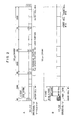
- Fig. 2 is a view illustrating cell structures provided on a transmission line and inside of the switcher
- Fig. 3 is a view detailing the cell structure provided inside of the switcher
- Fig. 4 is a block diagram showing arrangement of a transmission line interface on a receiving side
- Fig. 5 is a block diagram showing arrangement of a transmission line interface on a transmitting side.
- Fig. 6 is a view illustrating a frame format of SDH (Synchronous Digital Hierarchy).
- Fig. 1 shows arrangement of an essential portion of the ATM switcher designed according to the embodiment.
- the ATM switcher is designed to accommodate 256 I/O interface lines of 155.52Mb/s.
- 3 denotes a switching section for switching cells
- 2 denotes a receiving-side transmission-line interface section
- 4 denotes a transmitting-side transmission-line interface section for matching a transmitting interface with the transmission line.
- the receiving-side transmission-line interface section 2 provides a received cell buffer 21 and the transmitting-side transmission-line interface section 4 provides a transmitted cell buffer 41.
- I/O transmission line interfaces denote I/O transmission line interfaces and 121 and 122 denote internal highways.
- the I/O transmission line interfaces 111, 112 are designed so that the transmission format complies with the G.707 to 709 and the cell structure is 53B consisting of a header length of 5B and an information field length of 48B (see Fig. 2A).
- the ATM switcher serves to switch a cell train located on the I/O transmission lines into an inner cell train (see Fig. 2B) located on inner highways 121, 122 of totally 54B consisting of a header length of 6B and an information field length of 48B and switch the inner cells with each other on the switching section 3 as the switcher is controlling the write and read of the received cell buffer 21 and the transmitted cell buffer 41.
- the buffer 2l is located in the receiving-side transmission interface section 2 and the buffer 41 is located in the transmitting-side transmission interface section 4.
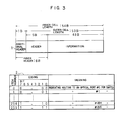
- Fig. 3 shows the arrangement of the inner cell in detail.
- the inner cell contains an additional one-byte (d-byte) header and an outer cell.
- the additional one-byte header has an output port number indicating an inner highway 122 to which the switching section 3 outputs the inner cell.
- the switching section 3 serves to route the inner cell to the output port indicated by the output port number.
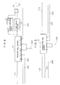
- Fig. 4 shows arrangement of the receiving-side transmission-line interface 2.
- the receiving-side transmission-line interface section 2 provides the received cell buffer 21, a header conversion table 23, a fixed delay section 24, and a header/information selector 25.
- the outer cell train transmitted on the input transmission line 111 is written in the received cell buffer 21 in synchronization to a write enable signal 201 and a write head signal 202.
- the write enable signal 201 indicates a pay load portion located on the input transmission line and the write cell head signal 202 indicating a head position of each outer cell located on the input transmission line 111.
- Both signals are extracted on a timing from the input signal on the receiving-side transmission line by a transmission frame terminal section (not shown) for performing some kinds of processing such as frame synchronization, detection of a parity check alarm and notification.
- the header portion and the information field portion are read from the received cell buffer 21 in synchronization to a readout cell head signal 203.
- the readout cell head signal 203 is generated on each inner-cell-delimiting timing placed on the inner highway 112 by a switcher timing generating section (not shown).
- the header portion is transmitted to the header conversion table 23 and the information field portion is transmitted to the fixed delay section 24.
- the header conversion table 23 serves to retrieve a header value to be updated and an additional header to be added from the header portion and then to transmit the information about the inner head used for the switcher to the header/information selector 25.
- the header value indicates a channel to which each cell belongs and the update of the header value indicates the conversion of a channel identification code, for example, on the input transmission line into a channel identification code, for example, used in the switcher.
- the information field portion transmitted to the fixed delay section 24 waits for a time required for accessing the header conversion table and a time corresponding to the additional header and then is sent to the header/information selector 25.
- the header/information selector 25 serves to merge the inner header portion with the information field portion and then send out the result as an inner cell train to the receiving-side inner highway 121.
- the input transmission line 111 When the outer cell is converted into the inner cell as mentioned above, the input transmission line 111 has a different cell rate than the inner highway 121. It is thus necessary to insert an empty cell as an inner cell. That is, if no cell to be read exists in the buffer when reading the received cell buffer 21, the reading is controlled so that an empty cell is inserted to the inner cell train. The empty cell is discarded in the switching section 3.
- a clock 200 used in the series of operations such as writing and reading can be assumed as a single cell rate sequence.
- Fig. 4 shows the arrangement of the transmitting-side transmission-line interface section 4.
- the transmitting-side transmitting-line interface section 4 provides the transmitted cell buffer 41.
- the written cell head signal 204 is generated on each inner-cell-delimiting timing placed on the inner highway 112 by the switcher timing generating section.
- the outer cell train is read out of the transmitted cell buffer 41 in synchronization to a readout enable signal 205 and a readout cell head signal 206 and then is sent to the pay load portion of the output transmission frame.
- the readout enable signal 205 indicates the pay load portion located on the output transmission path 112 and the readout cell head signal 206 indicates the head position of each outer cell located on the output transmission line 112 and both signals are generated in the transmission frame terminal section.
- a clock 200 used in the series of operations such as writing and reading can be assumed as a single cell rate sequence (the same cell rate sequence as the receiving side).
- the cell rate given on the transmitting-side inner highway 112 is 45 cell/125 ⁇ s and the cell rate given on the output transmission line 112 is about 44.15 cell/125 ⁇ s or a bit more.
- the switcher itself and the 1/0 transmission line are subject to at most 70 to 80% utilization rate. The mechanism is thus effected only when failure takes place. The switcher whose utilization rate is limited may reduce this mechanism.
- the ATM switcher can have the same cell rate sequence on both the I/O transmission line and the inner highways so that the cell rates are allowed to be same on the transmission line and the inner highways. If a simple buffer is provided, it is possible to switch the outer cell train located on the I/O transmission line to the inner cell train located on the inner highways or vice versa. It results in arranging the ATM switcher without having to provide a mechanism for complicated controls such as multiple-clocks control or intermittent control of the switching.
- routing control information such as an output port number
- the number of interface lines can be made smaller than the system for passing the routing control information on another line.
- the timing information of 8 kHz which is a basic timing of a digital network included in the transmission line frame, can be easily referenced by counting a cell-delimiting timing. It results in offering an effect that it allows a band to be easily assigned to a switch output port if the existing digital communication (e.g. a voice of 64 Kb/s) is provided on the ATM switcher for switching the line (The voice of 64 Kb/s is controlled to be output at each 2160 cells).
- the embodiment has met the relations (1) f x g - h x V (h is an integer or a fraction of an integer), (2) h x V x 125 x 10 -6 (k is an integer), and (3) b x h x V/f > v x V/c.
- the clock rate given on the I/O transmission line and the clock rate given on the inner highway can be placed on the same rate sequence.
- it may be designed to meet the relations (1) and (2) only, in which case the timing information, that is, a basic timing of 8 kHz of a digital network included in the transmission line frame can be easily referenced by counting the cell-delimiting timing even within the switcher. And, if it meets the relations (1), (2) and (3) like the foregoing embodiment, it results in enhancing a utilization rate of the outer cell.
- the communication processing device related to the invention has been described with reference to the ATM switcher. It goes without saying that the invention may be applied to a multiplexing device and a general packet switcher in addition to the ATM switcher. In the applications, the processing of the inner cell makes it possible to provide the similar effect.
- the present invention can offer a communication processing device such as a packet switcher which is capable of operating on a single clock rate sequence without having to perform the switching control in a complicated manner.
Landscapes
- Engineering & Computer Science (AREA)
- Computer Networks & Wireless Communication (AREA)
- Signal Processing (AREA)
- Data Exchanges In Wide-Area Networks (AREA)
Applications Claiming Priority (3)
| Application Number | Priority Date | Filing Date | Title |
|---|---|---|---|
| JP31598889A JP2964457B2 (ja) | 1989-12-05 | 1989-12-05 | 通信処理装置 |
| JP315988/89 | 1989-12-05 | ||
| JP31598889 | 1989-12-05 |
Publications (3)
| Publication Number | Publication Date |
|---|---|
| EP0436069A2 true EP0436069A2 (fr) | 1991-07-10 |
| EP0436069A3 EP0436069A3 (en) | 1995-01-11 |
| EP0436069B1 EP0436069B1 (fr) | 1999-11-03 |
Family
ID=18071991
Family Applications (1)
| Application Number | Title | Priority Date | Filing Date |
|---|---|---|---|
| EP19900115811 Expired - Lifetime EP0436069B1 (fr) | 1989-12-05 | 1990-08-17 | Méthode et dispositif de commutation de paquets de longueur fixe tels que des cellules ATM |
Country Status (5)
| Country | Link |
|---|---|
| US (1) | US5159591A (fr) |
| EP (1) | EP0436069B1 (fr) |
| JP (1) | JP2964457B2 (fr) |
| CA (1) | CA2023446C (fr) |
| DE (1) | DE69033340T2 (fr) |
Cited By (8)
| Publication number | Priority date | Publication date | Assignee | Title |
|---|---|---|---|---|
| EP0468818A2 (fr) * | 1990-07-27 | 1992-01-29 | Nec Corporation | Système de conversion de format de cellule ATM |
| EP0575656A1 (fr) * | 1992-06-26 | 1993-12-29 | Siemens Aktiengesellschaft | Méthode pour manipuler l'en-tête d'une cellule ATM |
| WO1994014266A1 (fr) * | 1992-12-15 | 1994-06-23 | Telefonaktiebolaget Lm Ericsson | Systeme de regulation de flux pour commutateurs de paquets |
| EP0606729A2 (fr) * | 1993-01-11 | 1994-07-20 | AT&T Corp. | Format interne étendu de cellules à ATM |
| EP0607672A2 (fr) * | 1993-01-11 | 1994-07-27 | AT&T Corp. | Dispositif de synchronisation de charge utile à ATM |
| EP0607673A2 (fr) * | 1993-01-11 | 1994-07-27 | AT&T Corp. | Commutateur à ATM |
| EP0616480A2 (fr) * | 1993-03-17 | 1994-09-21 | Roke Manor Research Limited | Système de communication entre réseau ATM et système de radio mobile |
| EP0634879A2 (fr) * | 1993-07-14 | 1995-01-18 | ATecoM GmbH | Dispositif et procédé pour le traitement de structures de données lors de leur passage à travers un noeud de réseau |
Families Citing this family (16)
| Publication number | Priority date | Publication date | Assignee | Title |
|---|---|---|---|---|
| US20020101871A1 (en) | 1991-01-31 | 2002-08-01 | Fujitsu Limited | Connectionless communication system |
| JPH0583291A (ja) * | 1991-09-19 | 1993-04-02 | Fujitsu Ltd | Atm試験方式 |
| EP0649583B1 (fr) * | 1992-04-06 | 1997-02-12 | Nortel Networks Corporation | Interface de noyau de commutateur a mode de transfert asynchrone |
| SE515274C2 (sv) * | 1992-11-09 | 2001-07-09 | Ericsson Telefon Ab L M | Paketväljare för telekommunikationsanläggning |
| FI92362C (fi) * | 1992-12-14 | 1994-10-25 | Nokia Telecommunications Oy | Menetelmä kehysvälitysverkon ylikuormitustilanteiden hallitsemiseksi sekä kehysvälitysverkon solmu |
| US6067408A (en) * | 1993-05-27 | 2000-05-23 | Advanced Micro Devices, Inc. | Full duplex buffer management and apparatus |
| US5428609A (en) * | 1994-01-03 | 1995-06-27 | At&T Corp. | STM-to-ATM converters |
| US5475679A (en) * | 1994-12-08 | 1995-12-12 | Northern Telecom Limited | Large capacity ATM switch |
| GB2337663B (en) * | 1995-03-31 | 2000-02-16 | Inmarsat Ltd | Communication method and apparatus |
| US5905727A (en) * | 1996-10-08 | 1999-05-18 | International Business Machines Corporation | Method and system for transmitting ATM cells on an ATM link |
| US6229808B1 (en) * | 1997-03-07 | 2001-05-08 | Advanced Micro Devices, Inc. | Method of communication for a computer using packet switches for internal data transfer |
| JP3537318B2 (ja) | 1998-07-24 | 2004-06-14 | 富士通株式会社 | 特定のコネクションの通信データを加工する交換機および交換方法 |
| US7103039B1 (en) | 2001-03-16 | 2006-09-05 | Cisco Technology, Inc. | Hardware load balancing through multiple fabrics |
| US7184403B1 (en) * | 2001-03-16 | 2007-02-27 | Cisco Technology, Inc. | Hardware load balancing through a single fabric |
| JP3908483B2 (ja) * | 2001-06-28 | 2007-04-25 | 富士通株式会社 | 通信装置 |
| US20050214389A1 (en) * | 2004-03-26 | 2005-09-29 | Council Of Scientific And Industrial Research | Beta-carotene enriched extract from water hyacinth eichhornia crassipes |
Citations (3)
| Publication number | Priority date | Publication date | Assignee | Title |
|---|---|---|---|---|
| EP0219049A2 (fr) * | 1985-10-07 | 1987-04-22 | Nec Corporation | Système de communication à commutation de paquets à grande vitesse avec commande du flux de bout en bout et avec retransmission |
| US4782478A (en) * | 1987-03-04 | 1988-11-01 | Bell Communications Research, Inc. | Time division circuit switch |
| EP0351818A2 (fr) * | 1988-07-22 | 1990-01-24 | Hitachi, Ltd. | Système de commutation ATM |
Family Cites Families (3)
| Publication number | Priority date | Publication date | Assignee | Title |
|---|---|---|---|---|
| US4670871A (en) * | 1985-06-27 | 1987-06-02 | American Telephone And Telegraph Company, At&T Bell Laboratories | Reliable synchronous inter-node communication in a self-routing network |
| CA1254982A (fr) * | 1986-05-14 | 1989-05-30 | Northern Telecom Limited | Methode de commutation d'informations et commutateur connexe |
| GB8724208D0 (en) * | 1987-10-15 | 1987-11-18 | Newman P | Self-routing switching element |
-
1989
- 1989-12-05 JP JP31598889A patent/JP2964457B2/ja not_active Expired - Fee Related
-
1990
- 1990-08-16 CA CA 2023446 patent/CA2023446C/fr not_active Expired - Fee Related
- 1990-08-17 US US07/569,025 patent/US5159591A/en not_active Expired - Lifetime
- 1990-08-17 DE DE69033340T patent/DE69033340T2/de not_active Expired - Fee Related
- 1990-08-17 EP EP19900115811 patent/EP0436069B1/fr not_active Expired - Lifetime
Patent Citations (3)
| Publication number | Priority date | Publication date | Assignee | Title |
|---|---|---|---|---|
| EP0219049A2 (fr) * | 1985-10-07 | 1987-04-22 | Nec Corporation | Système de communication à commutation de paquets à grande vitesse avec commande du flux de bout en bout et avec retransmission |
| US4782478A (en) * | 1987-03-04 | 1988-11-01 | Bell Communications Research, Inc. | Time division circuit switch |
| EP0351818A2 (fr) * | 1988-07-22 | 1990-01-24 | Hitachi, Ltd. | Système de commutation ATM |
Cited By (19)
| Publication number | Priority date | Publication date | Assignee | Title |
|---|---|---|---|---|
| EP0468818A3 (en) * | 1990-07-27 | 1992-09-09 | Nec Corporation | Atm cell format conversion system |
| EP0468818A2 (fr) * | 1990-07-27 | 1992-01-29 | Nec Corporation | Système de conversion de format de cellule ATM |
| US5341376A (en) * | 1990-07-27 | 1994-08-23 | Nec Corporation | ATM cell format conversion system |
| US5390174A (en) * | 1992-06-26 | 1995-02-14 | Siemens Aktiengesellschaft | Method for handling information contained in a header portion of message cells transmitted in asynchronous transfer mode |
| EP0575656A1 (fr) * | 1992-06-26 | 1993-12-29 | Siemens Aktiengesellschaft | Méthode pour manipuler l'en-tête d'une cellule ATM |
| WO1994014266A1 (fr) * | 1992-12-15 | 1994-06-23 | Telefonaktiebolaget Lm Ericsson | Systeme de regulation de flux pour commutateurs de paquets |
| CN1050250C (zh) * | 1992-12-15 | 2000-03-08 | L.M.埃利克逊电话股份有限公司 | 分组交换机的信息流控制系统和方法 |
| AU693427B2 (en) * | 1992-12-15 | 1998-07-02 | Telefonaktiebolaget Lm Ericsson (Publ) | Flow control system for packet switches |
| US5493566A (en) * | 1992-12-15 | 1996-02-20 | Telefonaktiebolaget L M. Ericsson | Flow control system for packet switches |
| EP0606729A2 (fr) * | 1993-01-11 | 1994-07-20 | AT&T Corp. | Format interne étendu de cellules à ATM |
| EP0607673A3 (en) * | 1993-01-11 | 1996-12-11 | At & T Corp | Asynchronous transfer mode (atm) switch fabric. |
| EP0607672A3 (en) * | 1993-01-11 | 1996-12-11 | At & T Corp | Asynchronous transfer mode (atm) payload synchronizer. |
| EP0606729A3 (en) * | 1993-01-11 | 1996-12-18 | At & T Corp | Asynchronous transfer mode (atm) expanded internal cell format. |
| EP0607673A2 (fr) * | 1993-01-11 | 1994-07-27 | AT&T Corp. | Commutateur à ATM |
| EP0607672A2 (fr) * | 1993-01-11 | 1994-07-27 | AT&T Corp. | Dispositif de synchronisation de charge utile à ATM |
| EP0616480A3 (fr) * | 1993-03-17 | 1994-10-26 | Roke Manor Research | Système de communication entre réseau ATM et système de radio mobile. |
| EP0616480A2 (fr) * | 1993-03-17 | 1994-09-21 | Roke Manor Research Limited | Système de communication entre réseau ATM et système de radio mobile |
| EP0634879A2 (fr) * | 1993-07-14 | 1995-01-18 | ATecoM GmbH | Dispositif et procédé pour le traitement de structures de données lors de leur passage à travers un noeud de réseau |
| EP0634879A3 (fr) * | 1993-07-14 | 1997-02-05 | Cadis Gmbh | Dispositif et procédé pour le traitement de structures de données lors de leur passage à travers un noeud de réseau. |
Also Published As
| Publication number | Publication date |
|---|---|
| CA2023446A1 (fr) | 1991-06-06 |
| EP0436069A3 (en) | 1995-01-11 |
| DE69033340D1 (de) | 1999-12-09 |
| CA2023446C (fr) | 1993-11-16 |
| JPH03175839A (ja) | 1991-07-30 |
| DE69033340T2 (de) | 2000-08-03 |
| US5159591A (en) | 1992-10-27 |
| EP0436069B1 (fr) | 1999-11-03 |
| JP2964457B2 (ja) | 1999-10-18 |
Similar Documents
| Publication | Publication Date | Title |
|---|---|---|
| US5159591A (en) | Packet communication method, packet communication device and packet switcher | |
| US5504742A (en) | Broadband ISDN remote multiplexer | |
| US5101404A (en) | Signalling apparatus for use in an ATM switching system | |
| US5220563A (en) | Device for the transmission by an asynchronous network, notably an atm type network, of signalling data, channel by channel, assembled in a multiframe transmitted synchronously in out-of-band mode | |
| CN87105673A (zh) | 三时隙数字用户线终端 | |
| EP0355797B1 (fr) | Appareil de signalisation pour utilisation dans un système de commutation ATM | |
| JPH02226926A (ja) | 多重チャネルpcmタイプのリング上にhdlcフレームを伝送するためのシステム | |
| US6208654B1 (en) | Cell multiplexing device for synchronous digital interface and method thereof | |
| US6393033B1 (en) | Method and apparatus for encapsulating ISDN data in a broadband network | |
| JPH07221764A (ja) | オーダワイヤ中継方式 | |
| KR19990013420A (ko) | 통계적 데이터 압축 방법 | |
| JP2951606B2 (ja) | 通信処理装置、パケッ卜交換機およびパケット処理方法 | |
| US5905734A (en) | Time slot interchanger and digital communications terminal for ISDN D-channel assembly | |
| KR100220638B1 (ko) | Atm 교환기와 ds1e 전송장치간의 정합장치 | |
| JP2751832B2 (ja) | Atm網および網構成装置 | |
| US6587478B1 (en) | Cell interleaving method in ATM switching system | |
| KR950035219A (ko) | 종합정보통신망과 근거리통신망 간의 망정합을 위한 게이트웨이 구현방법 및 시스템 | |
| JPS63209298A (ja) | 加入者線信号処理装置 | |
| KR950002509A (ko) | 종합 정보 통신망용 중용량 사설 교환기의 1차군 속도 인터페이스 장치 | |
| JPH0583289A (ja) | 揺らぎによる遅延時間削減方式 | |
| JPS6341259B2 (fr) | ||
| JP2927283B2 (ja) | Atmセルの無線送信方式 | |
| JPH0730584A (ja) | 音声パケット交換装置 | |
| McDonald et al. | Synthesis of a T-Carrier Bit Stream Processing System: An Integrated Transmission and Switching System | |
| JPH02224548A (ja) | Atmセル交換回路網 |
Legal Events
| Date | Code | Title | Description |
|---|---|---|---|
| PUAI | Public reference made under article 153(3) epc to a published international application that has entered the european phase |
Free format text: ORIGINAL CODE: 0009012 |
|
| 17P | Request for examination filed |
Effective date: 19900817 |
|
| AK | Designated contracting states |
Kind code of ref document: A2 Designated state(s): DE FR |
|
| PUAL | Search report despatched |
Free format text: ORIGINAL CODE: 0009013 |
|
| AK | Designated contracting states |
Kind code of ref document: A3 Designated state(s): DE FR |
|
| 17Q | First examination report despatched |
Effective date: 19960918 |
|
| GRAG | Despatch of communication of intention to grant |
Free format text: ORIGINAL CODE: EPIDOS AGRA |
|
| GRAG | Despatch of communication of intention to grant |
Free format text: ORIGINAL CODE: EPIDOS AGRA |
|
| GRAH | Despatch of communication of intention to grant a patent |
Free format text: ORIGINAL CODE: EPIDOS IGRA |
|
| GRAH | Despatch of communication of intention to grant a patent |
Free format text: ORIGINAL CODE: EPIDOS IGRA |
|
| GRAA | (expected) grant |
Free format text: ORIGINAL CODE: 0009210 |
|
| AK | Designated contracting states |
Kind code of ref document: B1 Designated state(s): DE FR |
|
| REF | Corresponds to: |
Ref document number: 69033340 Country of ref document: DE Date of ref document: 19991209 |
|
| ET | Fr: translation filed | ||
| PLBE | No opposition filed within time limit |
Free format text: ORIGINAL CODE: 0009261 |
|
| STAA | Information on the status of an ep patent application or granted ep patent |
Free format text: STATUS: NO OPPOSITION FILED WITHIN TIME LIMIT |
|
| 26N | No opposition filed | ||
| PGFP | Annual fee paid to national office [announced via postgrant information from national office to epo] |
Ref country code: FR Payment date: 20030617 Year of fee payment: 14 |
|
| PGFP | Annual fee paid to national office [announced via postgrant information from national office to epo] |
Ref country code: DE Payment date: 20030925 Year of fee payment: 14 |
|
| PG25 | Lapsed in a contracting state [announced via postgrant information from national office to epo] |
Ref country code: DE Free format text: LAPSE BECAUSE OF NON-PAYMENT OF DUE FEES Effective date: 20050301 |
|
| PG25 | Lapsed in a contracting state [announced via postgrant information from national office to epo] |
Ref country code: FR Free format text: LAPSE BECAUSE OF NON-PAYMENT OF DUE FEES Effective date: 20050429 |
|
| REG | Reference to a national code |
Ref country code: FR Ref legal event code: ST |