EP0429948B1 - Demodulator für ein phasenmoduliertes Signal und Radioempfänger mit einem solchen Demodulator - Google Patents
Demodulator für ein phasenmoduliertes Signal und Radioempfänger mit einem solchen Demodulator Download PDFInfo
- Publication number
- EP0429948B1 EP0429948B1 EP90121722A EP90121722A EP0429948B1 EP 0429948 B1 EP0429948 B1 EP 0429948B1 EP 90121722 A EP90121722 A EP 90121722A EP 90121722 A EP90121722 A EP 90121722A EP 0429948 B1 EP0429948 B1 EP 0429948B1
- Authority
- EP
- European Patent Office
- Prior art keywords
- digital signals
- polarity
- signal
- signals
- output
- Prior art date
- Legal status (The legal status is an assumption and is not a legal conclusion. Google has not performed a legal analysis and makes no representation as to the accuracy of the status listed.)
- Expired - Lifetime
Links
- 238000000034 method Methods 0.000 claims description 30
- 238000010276 construction Methods 0.000 description 18
- 238000010586 diagram Methods 0.000 description 16
- 239000000919 ceramic Substances 0.000 description 2
- 238000006243 chemical reaction Methods 0.000 description 2
- 230000015572 biosynthetic process Effects 0.000 description 1
- 230000000295 complement effect Effects 0.000 description 1
- 230000001934 delay Effects 0.000 description 1
- 238000001514 detection method Methods 0.000 description 1
- 238000005070 sampling Methods 0.000 description 1
Images


Classifications
-
- H—ELECTRICITY
- H04—ELECTRIC COMMUNICATION TECHNIQUE
- H04L—TRANSMISSION OF DIGITAL INFORMATION, e.g. TELEGRAPHIC COMMUNICATION
- H04L27/00—Modulated-carrier systems
- H04L27/18—Phase-modulated carrier systems, i.e. using phase-shift keying
- H04L27/22—Demodulator circuits; Receiver circuits
- H04L27/233—Demodulator circuits; Receiver circuits using non-coherent demodulation
- H04L27/2332—Demodulator circuits; Receiver circuits using non-coherent demodulation using a non-coherent carrier
-
- H—ELECTRICITY
- H03—ELECTRONIC CIRCUITRY
- H03D—DEMODULATION OR TRANSFERENCE OF MODULATION FROM ONE CARRIER TO ANOTHER
- H03D3/00—Demodulation of angle-, frequency- or phase- modulated oscillations
- H03D3/007—Demodulation of angle-, frequency- or phase- modulated oscillations by converting the oscillations into two quadrature related signals
- H03D3/008—Compensating DC offsets
-
- H—ELECTRICITY
- H04—ELECTRIC COMMUNICATION TECHNIQUE
- H04L—TRANSMISSION OF DIGITAL INFORMATION, e.g. TELEGRAPHIC COMMUNICATION
- H04L27/00—Modulated-carrier systems
- H04L27/10—Frequency-modulated carrier systems, i.e. using frequency-shift keying
- H04L27/14—Demodulator circuits; Receiver circuits
- H04L27/144—Demodulator circuits; Receiver circuits with demodulation using spectral properties of the received signal, e.g. by using frequency selective- or frequency sensitive elements
- H04L27/152—Demodulator circuits; Receiver circuits with demodulation using spectral properties of the received signal, e.g. by using frequency selective- or frequency sensitive elements using controlled oscillators, e.g. PLL arrangements
- H04L27/1525—Demodulator circuits; Receiver circuits with demodulation using spectral properties of the received signal, e.g. by using frequency selective- or frequency sensitive elements using controlled oscillators, e.g. PLL arrangements using quadrature demodulation
-
- H—ELECTRICITY
- H03—ELECTRONIC CIRCUITRY
- H03D—DEMODULATION OR TRANSFERENCE OF MODULATION FROM ONE CARRIER TO ANOTHER
- H03D2200/00—Indexing scheme relating to details of demodulation or transference of modulation from one carrier to another covered by H03D
- H03D2200/0001—Circuit elements of demodulators
- H03D2200/0025—Gain control circuits
-
- H—ELECTRICITY
- H03—ELECTRONIC CIRCUITRY
- H03D—DEMODULATION OR TRANSFERENCE OF MODULATION FROM ONE CARRIER TO ANOTHER
- H03D2200/00—Indexing scheme relating to details of demodulation or transference of modulation from one carrier to another covered by H03D
- H03D2200/0001—Circuit elements of demodulators
- H03D2200/0035—Digital multipliers and adders used for detection
-
- H—ELECTRICITY
- H03—ELECTRONIC CIRCUITRY
- H03D—DEMODULATION OR TRANSFERENCE OF MODULATION FROM ONE CARRIER TO ANOTHER
- H03D2200/00—Indexing scheme relating to details of demodulation or transference of modulation from one carrier to another covered by H03D
- H03D2200/0041—Functional aspects of demodulators
- H03D2200/005—Analog to digital conversion
-
- H—ELECTRICITY
- H03—ELECTRONIC CIRCUITRY
- H03D—DEMODULATION OR TRANSFERENCE OF MODULATION FROM ONE CARRIER TO ANOTHER
- H03D3/00—Demodulation of angle-, frequency- or phase- modulated oscillations
- H03D3/006—Demodulation of angle-, frequency- or phase- modulated oscillations by sampling the oscillations and further processing the samples, e.g. by computing techniques
Definitions
- the present invention relates to a demodulator and a radio receiver having such a demodulator and, more particularly, to a demodulator for digitizing an angle modulated reception signal and, thereafter, demodulating it, and also relates to a radio receiver.
- a ceramic discriminator, a quadrature demodulator, or the like has widely been used as a demodulator for detecting a deviation amount of an angle modulated reception input signal from a predetermined center frequency, thereby obtaining a demodulation signal.
- those demodulators need devices such as ceramic device, inductance device to shift the phase by 90°, and the like which are not suitable to be realized in an IC.
- a carrier to be processed is limited to a special frequency. Thus, there is a problem of miniaturization such that the application is limited to a heterodyne receiver or the like.
- an attention has been paid to a method of miniaturizing a circuit scale (realizing an IC) by using a direct conversion method as a receiving method whereby after two base band signals (hereinafter, referred to as an I signal and a Q signal) which have the same frequency as that of a reception wave as an input signal or an intermediate frequency wave and whose phases are mutually orthogonal and different by only ⁇ /2 radian were extracted, a channel is selected and a demodulating process is executed and by using a digital demodulator for demodulating the digital signals (I and Q signals) as a demodulator.
- a direct conversion method as a receiving method whereby after two base band signals (hereinafter, referred to as an I signal and a Q signal) which have the same frequency as that of a reception wave as an input signal or an intermediate frequency wave and whose phases are mutually orthogonal and different by only ⁇ /2 radian were extracted, a channel is selected and a demodulating process is executed and by using a digital demodulator for de
- Fig. 2 shows a schematic construction of a radio receiver to which the invention is applied.
- R(t) Acos ⁇ c t + ⁇ (t) ⁇
- An output signal of a local oscillator 14 has an angle frequency which is almost equal to the angle frequency ⁇ c of the reception carrier.
- a distribution phase shifter 15 distributes the output signal of the local oscillator 14 into two signals and, thereafter, converts a phase difference between the two output signals into ⁇ /2 radian.
- Two output signals LI and LQ of the distribution phase shifter 15 are input to mixers 16 and 17, respectively.
- Each of the reception signals R(t) is frequency converted. Since the center frequency of a desired reception signal and a local oscillating frequency are almost equal, a desired receiving frequency after completion of the frequency conversion is set to about a few kHz.
- the square values of the I signal and Q signal are calculated by square calculators 23 and 24 in accordance with the equations (4) and (5) to obtain I'(t) and Q'(t).
- the sum of the two squared values is calculated by an adder 25.
- the square root of the sum as an output signal of the adder 25 is calculated by a square root calculator 26.
- An I' signal and a Q' signal are obtained by dividing the I signal and Q signal by the value of the square root by two dividers 27 and 28, respectively.
- the differentiated values of the I' signal and Q' signal are obtained by two differentiators 29 and 30 on the basis of the equations (6) and (7).
- a DI' signal and a DQ' signal are obtained by two multipliers 31 and 32 on the basis of the equations (8) and (9).
- the demodulation output O(t) signal is derived.
- the divider is a kind of multiplier
- the limiter 1 and the demodulator 2 shown in Fig. 3 are constructed by a dedicated digital circuit instead of a digital processor, total six multipliers (23, 24, 27, 28, 31, and 32) including the square and the division are necessary.
- An ordinary multiplier is constructed by a combination of adders. In the case of executing a multiplying process at a high speed, its circuit scale is almost equal to the scale of the circuit in which the number of bits of the data was multiplied to the adder.
- the differentiator can be constructed by a differential circuit and its component elements are a delay circuit and a subtracter. Since the subtacter is a kind of adder, the demodulator shown in Fig. 3 needs total four adders (26, 29, 30, and 33) including the subtracter.
- the delay circuit is constructed by a shift register. Further, an inverse calculator and a square root calculator are needed for division.
- the digital signal processing circuit can be realized as an IC as mentioned above, if it is merely constructed as an IC, its circuit scale increases. On the other hand, even if the circuit stability is improved and the circuit scale can be slightly miniaturized due to the formation of an IC, there is also a possibility such that a disadvantage occurs from a viewpoint of an electric power consumption as compared with the case of an analog signal process. Particularly, in the case of using such a kind of demodulator in a small receiver such as a mobile radio receiver, a large electric power consumption causes a serious drawback.
- the invention has the advantage, that limiters in the demodulator and the radio receiver can be implemented by digital circuits including no multiplier.
- a limiter for amplitude limiting each of an I signal and a Q signal as two digital signals which are obtained from an angle modulation wave and have a mutually orthogonal phase relation is constructed by: an absolute value circuit for obtaining absolute values of the I and Q signals; a synthesizer for outputting the sum of the absolute values of the I and Q signals or a larger one of the absolute values of the I and Q signals; a scaler for changing amplitudes of the I and Q signals; and a controller for controlling the scaler by an output of the synthesizer.
- the absolute value circuit there is used a circuit for inverting the bit in accordance with the positive or negative sign of each of the input signals for the I and Q signals which are input.
- the scaler is constructed by a shift register and an adder for realizing an equation in which an inverse number of the output of the synthesizer is approximately developed to the sum of the values of the powers of 2.
- the bit shifting process and the addition according to the value of the power are executed to each of the I and Q signals and the resultant I' and Q' signals are used as limiter outputs.
- the demodulator is constructed so as to obtain a relative phase rotating direction of the amplitude limited I' and Q' signals and thereby to obtain a demodulation output.
- a differential value between each of the I' and Q' signals and the data which is preceding by one sampling time is first obtained. Then, the polarity of the differential value of the Q' signal is inverted in accordance with the value of the I' signal. Similarly, the polarity of the differential value of the I' signal is inverted in accordance with the value of the Q' signal. Finally, the difference between the two outputs is obtained and used as a demodulation signal O(t).
- I'(t) I(t)/M( I(t) , Q(t) )
- Q'(t) Q(t)/M( I(t) , Q(t) )
- a function M(a, b) denotes that either larger one of a and b is selected. That is, the equations (13) and (14) execute the scaling by either larger one of the absolute values of the I and Q signals.
- two absolute value calculators, two dividers, and one comparator are fundamentally needed.
- a point that the limiter which is constructed by the second approximate equation differs from the limiter which is constructed by the first approximate equation is that a comparator is used in place of the adder. Since the comparator comprises a subtracter and a polarity detector, the circuit scale is almost equal.
- the divider which is necessary generally comprises an inverse calculator and a multiplier.
- an approxiamte calculation for the division is further executed and the circuit scale is reduced.
- the divisor in each of the equations (11) to (14) is represented by D and is expressed by a binary number.
- An inverse number of D is approximated by the sum of the values of the powers of 2 by using the following approximate equations.
- the calculations of the equations (11) to (14) are the approximate equation of the equation (16) and the product of the I and Q signals.
- the power of 2 can be accomplished by the bit shift process.
- the limiter since the coefficient is equal to 1 or 0, the limiter has a construction of a combination of a bit shifter and an adder. Therefore, the circuit scale can be further reduced as compared with the approximate calculation using the above divider.
- the calculating accuracy can be raised. Since the circuit scale increases with an increase in number of terms, it is necessary to design the limiter by comparing and considering the calculating accuracy and the limitation of the circuit scale.
- the demodulator can be accomplished by the differential operations in the case of constructing a digital signal processing circuit according to the differentiating operations of the equations (6) and (7).
- Such differential operations are expressed by the following equations with respect to the DI and DQ signals.
- DI(t) I'(t) - I'(t - 1)
- DQ(t) Q'(t) - Q'(t - 1)
- DI'(t) P(Q') ⁇ DI(t)
- DQ'(t) P(I') ⁇ DQ(t)
- P(I') corresponds to the polarity of the I' signal
- P(Q') corresponds to the polarity of the Q' signal, respectively. If the polarity is positive, +1 is applied. If the polarity is negative, -1 is applied.
- a difference between the DQ' signal and the DI' signal is calculated and is set to a demodulation signal O(t).
- O(t) DQ'(t) - DI'(t)
- processes for the DI and DQ signals are executed on the basis of the polarities of the I' and Q' signals, thereby obtaining the O signal.
- DQ(t) sin ⁇ (t) ⁇ /D(t) - sin ⁇ (t-1) ⁇ /D(t-1)
- the modulating operation can be executed by the above approximating calculations. Even for another combination of the I' and Q' signals, a similar demodulation output O signal can be obtained in accordance with table of Fig. 12.
- the demodulator of the invention can be constructed by: two differentiators (differential circuits) each having a shift register and a subtracter; level comparators; polarity inverters; and a subtracter. Since no multiplier is used, the circuit scale can be remarkably reduced.
- Fig. 1 is a constructional diagram of an embodiment of a demodulator according to the invention.
- the limiter 1 comprises: a synthesizer 3 to obtain a synthetic wave of an I signal and a Q signal; two scalers 5 and 6 to apply an amplitude limitation to the I and Q signals; and a controller 4 to control the scalers 5 and 6 in accordance with an output from the synthesizer 3.
- the demodulator 2 comprises: two differentiators 7 and 8 to obtain differentiated values of an I' signal and a Q' signal as output signals of the scalers 5 and 6 of the limiter 1; two polarity detectors 9 and 10 to detect the polarities of the I' and Q' signals and determine the operations of polarity inverters; two polarity inverters 11 and 12 to change the polarities of the differentiated values of the I' and Q' signals in accordance with information from the polarity detectors 9 and 10; and a subtracter 13 to obtain a difference between output signals of the two polarity detectors.
- Fig. 4 is a constructional diagram of the embodiment of the limiter 1 which is constructed on the basis of the equations (11) and (12).
- the limiter comprises the synthesizer 3 and the two dividers 27 and 28.
- the synthesizer 3 comprises two absolute value calculators 34 and 35 and the adder 25 from the equations (11) and (12).
- the two dividers 27 and 28 correspond to the scalers 5 and 6 in Fig. 1. Since the limiting operation is realized by the division, in the circuit construction of Fig. 4, the output signal of the synthesizer 3 is used as a divisor of each of the two dividers 27 and 28. Therefore, the devices corresponding to the controller 4 in Fig. 1 includes two dividers 27 and 28.
- Fig. 5 is a constructional diagram of an embodiment of the limiter 1 which is constructed on the basis of the equations (13) and (14) and differs from the limiter 1 of Fig. 4 with respect to the construction of the synthesizer 3.
- the comparator 36 operates so as to select either larger one of the absolute values of the 1 and Q signals as outputs of the two absolute value calculators 34 and 35.
- the comparator 36 comprises: for instance, a subtracter to obtain a difference between two signals; a polarity detector to discriminate the magnitudes of the absolute values of the two signals on the basis of the polarity of the result of the difference; and a selector to output.
- the operation as a limiter is similar to that of the limiter shown in Fig. 4.
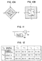
- Figs. 6a to 6C are diagrams showing the correlations between the outputs which are obtained by the ideal limiting operations shown in the equations (4) and (5) and the outputs which are derived by the limiting operations according to the approximate calculations shown in the equations (11) to (14).
- An axis of abscissa denotes the I' signal as a limiter output.
- An axis of ordinate indicates the Q' signal.
- Fig. 6A shows an ideal limiter output which is expressed by the equations (4) and (5) and a true circle is drawn.
- Fig. 6B shows a limiter output which is expressed by the equations (11) and (12) and a rhombus is drawn.
- FIG. 6C shows a limiter output which is expressed by the equations (13) and (14) and a square is drawn. If the absolute values are eliminated, the shape of Fig. 6C is fundamentally the same as that of Fig. 6B because Fig. 6C is derived by rotating the relative phases of the I' and Q' signals in Fig. 6B by 45°. For the ideal characteristics of Fig. 6A, a deviation from the true circle corresponds to an error of the approximate calculation of Fig. 6B or 6C. As mentioned above, the limiters shown in Figs. 4 and 5 need the dividers.
- Fig. 7 shows a construction of an embodiment of a limiter according to the invention.
- the scalers 5 and 6 are constructed without using any divider.
- the limiter of Fig. 7 comprises: the synthesizer 3 which is constructed by an absolute value sum calculator; the two scalers 5 and 6; and the controller 4.
- the synthesizer 3 operates in a manner similar to the synthesizer 3 shown in Fig. 4 and obtains the sum of the absolute values of the input I and Q signals.
- Each of the two scalers 5 and 6 executes the processors of the equations (16), (11), and (12) to the I and Q signals and performs the limiting operation.
- the scaler 5 comprises: four shift registers 37 to 40; three selectors 41 to 43; and four adders 44 to 47.
- each term of the right side of the equation (16) is allocated from the upper stage of the scaler.
- the controller 4 obtains a value of k in the equation (16) on the basis of the equation (16) in accordance with the output of the synthesizer 3 and sets shift amounts of the shift registers 37 to 40. That is, a bit shift amount of the shift register 37 is set to k. The bit shift amount is sequentially increased one bit by one and the bit shift amount of the shift register 40 is set to k + 3.
- the controller 4 also executes the similar control to the scaler 6.
- the synthesizer 3 in Fig. 5 can be used in place of the synthesizer 3.
- Fig. 8 is a diagram showing a construction of another embodiment of the scaler 5.
- the embodiment is used in the case where the I signal or the Q signal is serial data.
- the fundamental operations of selectors 49 to 51 and adders 52 to 55 are similar to those of the selectors 41 to 43 and the adders 44 to 47 shown in Fig. 7 except that parallel data is handled as signals.
- a variable shift register 48 is provided for the shift registers and the shift amounts are switched in accordance with the signal from the controller.
- Output bits outputted to the selectors 49 to 51 are sequentially shifted one bit by one to the adder 52 on the basis of the equation (16). Due to this, the circuit scale of the shift register section can be reduced.
- Fig. 9 shows a construction of an embodiment of the scaler 5 which can reduce the circuit scale.
- the construction of Fig. 9 is used in the case where the I and Q signals are serial data.
- a variable shift register 56 executes the first scaling process to the I signal.
- the bit shift amount in the variable shift register 56 is switched in accordance with the information from the synthesizer 3 and the controller 4.
- the fundamental operations of a fixed shift register 57, the selectors 49 to 51, and the adders 52 to 55 are similar to those of the scaler 5 shown in Fig. 8.
- a length of the shift register 57 is fixed and the bit shifting process corresponding to the value of k mentioned above can change the circuit scale and the output data length in accordance with the distribution of the bits to the variable shift register 56 and the fixed shift register 57.
- a circuit including the variable shift register 56 shown in Fig. 9 is the simplest scaler circuit.
- the circuit corresponds to that the approximate calculation is executed by using only the first term, that is, 2 k of the right side of the equation (16).
- Figs. 10A and 10B show the relations between the limiter output signals I' and Q' in the above case.
- each of the differentiators 7 and 8 is constructed by the difference circuit shown in Fig. 11 on the basis of the equations (17) and (18).
- a delay circuit 58 is constructed by a shift register and delays an input signal by a time of one sample. If the input signal is serial data, the delay circuit 58 is constructed by shift registers of the number corresponding to one word. If the input signal is parallel data, the delay circuit 58 is constructed by one shift register of the bits corresponding to one word.
- a subtracter 59 is constructed by an adder.
- Each of the polarity detectors 9 and 10 is constructed by a circuit for holding the polarity bit of the input signal. In this case, if data has a complement indication of 2, when the input data is positive, the output is set to 0. On the contrary, if the input data is negative, the output is set to 1. Therefore, the results obtained by the polarity detectors 9 and 10 correspond to P(I') and P(Q') in the equations (20) and (21). However, in the equations (20) and (21), P(I') and P(Q') are equal to 1 or -1.
- the polarity inverters 11 and 12 invert the polarities of the DI and DQ signals in accordance with the data from the polarity detectors 9 and 10. As mentioned above, the processes are executed in accordance with a combination of the circuit A in the table shown in Fig. 12. For example, if the polarity of the Q' signal is positive and the output of the polarity detector 10 is equal to 0, the polarity inverter 11 directly outputs the input DI signal as a DI' signal. On the other hand, if the polarity of the Q' signal is negative and the output of the polarity detector is equal to 1, the polarity inverter 11 inverts the polarity of the input DI signal and outputs as a DI' signal.
- a practical method of inverting the polarity is similar to the method which is used in the absolute value calculators 34 and 35 mentioned above. Due to this, the processes corresponding to the above equations (20) and (21) are executed by the polarity inverters 11 and 12, so that the DI' and DQ' signals are derived. Finally, by obtaining a difference between the DQ' and DI' signals by the subtracter 13, the process corresponding to the equation (22) is performed, so that the O(t) signal is obtained as a demodulation output.
- a typical example of the subtracter 13 is constructed by a combination of the polarity inverter and the adder. It is advantageous to construct the subtracter 13 by only the adders in consideration of the reduction of the circuit scale.
- the subtracter 13 can be constructed by only the adders. That is, when the Q' signal is positive and the output of the polarity detector 10 is equal to 0, it is sufficient to invert the polarity of the DI signal by the polarity inverter 11.
- the number of multipliers which construct the demodulator can be remarkably reduced. Therefore, in the case of constructing the demodulator by an IC, the number of component devices is reduced and the electric power consumption is reduced.
- the demodulator of the invention is effective means when it is applied to a small receiver such as a portable radio receiver or the like.
Landscapes
- Engineering & Computer Science (AREA)
- Computer Networks & Wireless Communication (AREA)
- Signal Processing (AREA)
- Physics & Mathematics (AREA)
- Spectroscopy & Molecular Physics (AREA)
- Power Engineering (AREA)
- Digital Transmission Methods That Use Modulated Carrier Waves (AREA)
Claims (8)
- Demodulatorvorrichtung zur Demodulation eines ersten und eines zweiten digitalen Signals S (I, Q), die aus einer empfangenen winkelmodulierten Welle erzeugt sind und deren Phasen zueinander rechtwinklig sind, aufweisend:einen Begrenzer (1) zur Amplitudenbegrenzung des ersten und des zweiten digitalen Signals, undeinen Demodulator (2) zur Demodulation eines Ausgangssignals des Begrenzers (1),dadurch gekennzeichnet, daß der Begrenzer (1) aufweist:ein Paar erster Schaltungen (34, 35), um Absolutwerte des ersten und des zweiten digitalen Signals zu erhalten,eine zweite Schaltung (25, 36) zur Ausgabe der Summe oder des größeren der genannten Absolutwerte als Divisor D,eine Steuerung (4) zur Lieferung von Schiebesteuer- und Auswahlsteuersignalen auf der Grundlage eines Binärwerts des Divisors D, undein Paar Skalierer (5, 6; 27, 28), von denen jeder zur Änderung der Amplitude eines entsprechenden der ersten und zweiten digitalen Signale (I, Q) entsprechend den Steuersignalen vorgesehen ist und aufweist:eine Schieberegistereinrichtung (37 bis 40, 48, 56, 57) zum Verschieben eines Binärwerts des entsprechenden digitalen Signals S um k, k + 1, ... und k + i Bits entsprechend der Schiebesteuersignale, um auf parallele Weise eine Vielzahl digitaler Signale S · 2-k, S · 2-(k+1), ... und S · 2-(k+i) zu bilden, wobei k so gewählt ist, daß 2k-1 ≤ D < 2k und i eine die Rechengenauigkeit bestimmende ganze Zahl darstellt, undeine Digitalschaltungseinrichtung (41 bis 47, 49 bis 59), um Signale aufzusummieren, die aus der genannten Vielzahl digitaler Signale entsprechend den Auswahlsteuersignalen ausgewählt werden, die von dem Bitmuster des Divisors D so abhängen, daß die erhaltene Summe ein Näherungswert des entsprechenden digitalen Signals S dividiert durch den Divisor D darstellt.
- Vorrichtung nach Anspruch 1, wobei jeder Skalierer (5, 6; 27, 28) aufweist:mehrere Schieberegister (38, 39, 40) zur vorübergehenden Speicherung des ersten und des zweiten digitalen Signals, wobei die Bitverschiebegrößen der Schieberegister unterschiedlich sind,mehrere Auswähler (41 bis 43) die mit den Schieberegistern verbunden sind und entsprechend den Steuersignalen ein/aus-gesteuert werden, undmehrere Addierer (45-47), die mit den Auswählern verbunden sind und von denen jeder Addierer eine Ausgabe des mit ihm verbundenen Auswählers und eine Ausgabe des anderen Addierers summiert.
- Vorrichtung nach Anspruch 1, wobei die Skalierer umfassen:
mehrere Skalierschaltungen (56, 57) die jeweils einen Skaliervorgang entsprechend einer von der Steuerung (4) erhaltenen Information durchführen und die niedrigwertigen Bits einer Ausgabe verarbeiten und die Zahl der Bits von Ausgabedaten auf einen konstanten Wert festlegen und die Daten als Eingabesignal an die Skalierschaltung der nächsten Stufe geben. - Vorrichtung nach einem der Ansprüche 1 bis 3, wobei die ersten Schaltungen (34, 35) aus Polaritätsdetektoren zur Feststellung der Polaritäten des entsprechenden ersten und zweiten digitalen Signals und aus Polaritätsumkehrern zur Gewinnung des ersten und des zweiten Absolutwerts durch Invertieren der Polaritäten des ersten und des zweiten digitalen Signals entsprechend der für das erste und das zweite digitale Signal festgestellten Polaritäten aufgebaut sind, und
wobei die zweite Schaltung (25) aus einer Synthetisierschaltung zur Ausgabe der Summe des ersten und des zweiten Absolutwerts aufgebaut ist. - Vorrichtung nach einem der Ansprüche 1 bis 3, wobei die erste Schaltung (34, 35) aus Polaritätsdetektoren zur Gewinnung der Polaritäten des entsprechenden ersten und zweiten digitalen Signals und aus Polaritätsumkehrern zur Gewinnung des ersten und des zweiten Absolutwerts durch Umkehrung der Polaritäten des ersten und zweiten digitalen Signals entsprechend den für das erste und zweite digitale Signal erfaßten Polaritäten aufgebaut ist, und
die zweite Schaltung (36) aus einer Schaltung zur Ausgabe des größeren des ersten und zweiten Absolutwerts aufgebaut ist. - Vorrichtung nach einem der Ansprüche 1 bis 5, wobei die Skalierer (5, 6, 27, 28) so arbeiten, daß mindestens eine der Amplituden des ersten und des zweiten digitalen Signals entsprechend dem Steuersignal nahezu konstant wird.
- Vorrichtung nach einem der Ansprüche 1 bis 6, wobei der Demodulator (2) aufweist:einen ersten und einen zweiten Polaritätsdetektor (9, 10) zur entsprechenden Erfassung der Polaritäten des ersten und des zweiten digitalen Signals, deren Amplituden von dem Begrenzer begrenzt wurden,einen ersten und einen zweiten Differenzierer (7, 8) zur Differenzierung des in der Amplitude begrenzten ersten und zweiten digitalen Signals,einen ersten Polaritätsumkehrer (11) zur Änderung der Polarität einer Ausgabe des ersten Differenzierers mittels einer Ausgabe des zweiten Polaritätsdetektors,einen zweiten Polaritätsumkehrer (12) zur Änderung der Polarität einer Ausgabe des zweiten Differenzierers mittels einer Ausgabe des ersten Polaritätsdetektors, undeinen Subtrahierer (13) zur Ausgabe einer Differenz zwischen den Ausgaben des ersten und des zweiten Polaritätsumkehrers als Demodulationssignal.
- Radioempfänger mit einer Demodulatorvorrichtung nach einem der Ansprüche 1 bis 7 zur Demodulation einer empfangenen winkelmodulierten Welle.
Applications Claiming Priority (2)
| Application Number | Priority Date | Filing Date | Title |
|---|---|---|---|
| JP1295000A JP2806997B2 (ja) | 1989-11-15 | 1989-11-15 | 復調器 |
| JP295000/89 | 1989-11-15 |
Publications (3)
| Publication Number | Publication Date |
|---|---|
| EP0429948A2 EP0429948A2 (de) | 1991-06-05 |
| EP0429948A3 EP0429948A3 (en) | 1992-10-21 |
| EP0429948B1 true EP0429948B1 (de) | 1997-05-28 |
Family
ID=17815042
Family Applications (1)
| Application Number | Title | Priority Date | Filing Date |
|---|---|---|---|
| EP90121722A Expired - Lifetime EP0429948B1 (de) | 1989-11-15 | 1990-11-13 | Demodulator für ein phasenmoduliertes Signal und Radioempfänger mit einem solchen Demodulator |
Country Status (4)
| Country | Link |
|---|---|
| US (1) | US5079513A (de) |
| EP (1) | EP0429948B1 (de) |
| JP (1) | JP2806997B2 (de) |
| DE (1) | DE69030803D1 (de) |
Families Citing this family (11)
| Publication number | Priority date | Publication date | Assignee | Title |
|---|---|---|---|---|
| JP3087459B2 (ja) * | 1991-09-27 | 2000-09-11 | 松下電器産業株式会社 | Fskデータ復調器 |
| JP2730346B2 (ja) * | 1991-09-30 | 1998-03-25 | 日本電気株式会社 | 分周回路 |
| US5414735A (en) * | 1993-04-26 | 1995-05-09 | Ford Motor Company | Method and apparatus for normalizing components of a complex signal |
| FR2714783B1 (fr) * | 1993-12-30 | 1996-02-09 | Thomson Csf | Procédé et dispositif de démodulation numérique à différentiation de phase et système de communication hyperfréquence appliqué notamment au péage automatique sur voies de circulation payantes. |
| SE504341C2 (sv) * | 1995-05-22 | 1997-01-20 | Ericsson Telefon Ab L M | Förfarande och anordning vid fasmodulerade signaler |
| JP3033708B2 (ja) * | 1997-04-21 | 2000-04-17 | 埼玉日本電気株式会社 | ピーククリッピング回路および該ピーククリッピング回路を有する直交変調送信機 |
| JP4083861B2 (ja) * | 1998-03-06 | 2008-04-30 | 株式会社日立国際電気 | ディジタル信号伝送装置 |
| US6081822A (en) * | 1998-03-11 | 2000-06-27 | Agilent Technologies, Inc. | Approximating signal power and noise power in a system |
| US6304136B1 (en) * | 1999-03-03 | 2001-10-16 | Level One Communications, Inc. | Reduced noise sensitivity, high performance FM demodulator circuit and method |
| US6127884A (en) * | 1999-05-24 | 2000-10-03 | Philips Electronics North America Corp. | Differentiate and multiply based timing recovery in a quadrature demodulator |
| JP5137793B2 (ja) * | 2008-11-26 | 2013-02-06 | 日本無線株式会社 | レベル調整回路 |
Family Cites Families (6)
| Publication number | Priority date | Publication date | Assignee | Title |
|---|---|---|---|---|
| GB2143386B (en) * | 1983-07-14 | 1987-01-14 | Standard Telephones Cables Ltd | Radio receiver |
| CH667170A5 (de) * | 1984-12-07 | 1988-09-15 | Industrieorientierte Forsch | Verfahren zur detektion der information eines empfangssignales, insbesondere mit frequenzumtastung. |
| JP2829605B2 (ja) * | 1985-09-03 | 1998-11-25 | モトローラ・インコーポレーテッド | ディジタル無線周波受信機 |
| GB2213662A (en) * | 1987-12-11 | 1989-08-16 | Philips Electronic Associated | Data demodulator carrier phase-error detector |
| US4833416A (en) * | 1988-03-30 | 1989-05-23 | Motorola, Inc. | QPSK/BPSK demodulator |
| JP6338890B2 (ja) | 2014-03-07 | 2018-06-06 | 東日本旅客鉄道株式会社 | 取水装置 |
-
1989
- 1989-11-15 JP JP1295000A patent/JP2806997B2/ja not_active Expired - Fee Related
-
1990
- 1990-11-13 DE DE69030803T patent/DE69030803D1/de not_active Expired - Lifetime
- 1990-11-13 EP EP90121722A patent/EP0429948B1/de not_active Expired - Lifetime
- 1990-11-15 US US07/612,982 patent/US5079513A/en not_active Expired - Lifetime
Also Published As
| Publication number | Publication date |
|---|---|
| US5079513A (en) | 1992-01-07 |
| DE69030803D1 (de) | 1997-07-03 |
| JP2806997B2 (ja) | 1998-09-30 |
| JPH03157033A (ja) | 1991-07-05 |
| EP0429948A2 (de) | 1991-06-05 |
| EP0429948A3 (en) | 1992-10-21 |
Similar Documents
| Publication | Publication Date | Title |
|---|---|---|
| JP3363025B2 (ja) | デジタル複素フェーザジェネレータおよびデジタル受信機における両方向周波数変換の方法 | |
| EP0429948B1 (de) | Demodulator für ein phasenmoduliertes Signal und Radioempfänger mit einem solchen Demodulator | |
| GB2225680A (en) | Complex digital sampling converter for demodulator | |
| US4887280A (en) | System for detecting the presence of a signal of a particular data rate | |
| US5521559A (en) | Signal oscillator, FM modulation circuit using the same, and FM modulation method | |
| US5640427A (en) | Demodulator | |
| US5369374A (en) | Differential detection demodulator | |
| US4674105A (en) | Digital signal processor | |
| US4942592A (en) | Synchronous receiver for minimum shift keying transmission | |
| US5517689A (en) | Phase detecting method and phase detector and FM receiver using phase detecting method | |
| US6011816A (en) | Direct demodulation method and apparatus | |
| US5578947A (en) | Delayed detection type demodulator | |
| EP0695028B1 (de) | Signalsummiereinrichtung in kleinem Massstab und differentielle Detektionseinrichtung | |
| US4608540A (en) | Phase-shift keying demodulator | |
| EP0412291B1 (de) | Quadraturempfänger für FSK-Signale mit Frequenzverschiebungskompensation | |
| EP0198701B1 (de) | Phasendetektionsschaltung | |
| EP0488624B1 (de) | Eine digitale Schaltung zur Quadraturphasenfeststellung | |
| JP3394788B2 (ja) | 周波数弁別器 | |
| JP2518860B2 (ja) | 位相同期回路 | |
| US8184746B2 (en) | Simplified de-rotation in digital FM demodulator architectures | |
| EP0434689B1 (de) | Synchroner empfänger für msk-übertragung | |
| JP3178277B2 (ja) | 直接変換受信機 | |
| EP0996263B1 (de) | Schaltung zur Rechnung der Steuerung einer Signalpunktordnung | |
| JPH066397A (ja) | 遅延検波器 | |
| SU1298946A1 (ru) | Устройство автоподстройки несущей частоты |
Legal Events
| Date | Code | Title | Description |
|---|---|---|---|
| PUAI | Public reference made under article 153(3) epc to a published international application that has entered the european phase |
Free format text: ORIGINAL CODE: 0009012 |
|
| AK | Designated contracting states |
Kind code of ref document: A2 Designated state(s): DE GB |
|
| PUAL | Search report despatched |
Free format text: ORIGINAL CODE: 0009013 |
|
| AK | Designated contracting states |
Kind code of ref document: A3 Designated state(s): DE GB |
|
| 17P | Request for examination filed |
Effective date: 19930225 |
|
| 17Q | First examination report despatched |
Effective date: 19941012 |
|
| GRAG | Despatch of communication of intention to grant |
Free format text: ORIGINAL CODE: EPIDOS AGRA |
|
| GRAH | Despatch of communication of intention to grant a patent |
Free format text: ORIGINAL CODE: EPIDOS IGRA |
|
| GRAH | Despatch of communication of intention to grant a patent |
Free format text: ORIGINAL CODE: EPIDOS IGRA |
|
| GRAA | (expected) grant |
Free format text: ORIGINAL CODE: 0009210 |
|
| AK | Designated contracting states |
Kind code of ref document: B1 Designated state(s): DE GB |
|
| REF | Corresponds to: |
Ref document number: 69030803 Country of ref document: DE Date of ref document: 19970703 |
|
| PG25 | Lapsed in a contracting state [announced via postgrant information from national office to epo] |
Ref country code: DE Effective date: 19970829 |
|
| PLBE | No opposition filed within time limit |
Free format text: ORIGINAL CODE: 0009261 |
|
| STAA | Information on the status of an ep patent application or granted ep patent |
Free format text: STATUS: NO OPPOSITION FILED WITHIN TIME LIMIT |
|
| 26N | No opposition filed | ||
| REG | Reference to a national code |
Ref country code: GB Ref legal event code: IF02 |
|
| PGFP | Annual fee paid to national office [announced via postgrant information from national office to epo] |
Ref country code: GB Payment date: 20021029 Year of fee payment: 13 |
|
| PG25 | Lapsed in a contracting state [announced via postgrant information from national office to epo] |
Ref country code: GB Free format text: LAPSE BECAUSE OF NON-PAYMENT OF DUE FEES Effective date: 20031113 |
|
| GBPC | Gb: european patent ceased through non-payment of renewal fee |
Effective date: 20031113 |