EP0421608A2 - Methode zur Erzeugung eines Halbleiterverbindung-Übergitters vom vertikaler Typ - Google Patents
Methode zur Erzeugung eines Halbleiterverbindung-Übergitters vom vertikaler Typ Download PDFInfo
- Publication number
- EP0421608A2 EP0421608A2 EP90309635A EP90309635A EP0421608A2 EP 0421608 A2 EP0421608 A2 EP 0421608A2 EP 90309635 A EP90309635 A EP 90309635A EP 90309635 A EP90309635 A EP 90309635A EP 0421608 A2 EP0421608 A2 EP 0421608A2
- Authority
- EP
- European Patent Office
- Prior art keywords
- layer
- compound semiconductor
- substrate
- atomic
- gas
- Prior art date
- Legal status (The legal status is an assumption and is not a legal conclusion. Google has not performed a legal analysis and makes no representation as to the accuracy of the status listed.)
- Withdrawn
Links
Images





Classifications
-
- H—ELECTRICITY
- H10—SEMICONDUCTOR DEVICES; ELECTRIC SOLID-STATE DEVICES NOT OTHERWISE PROVIDED FOR
- H10P—GENERIC PROCESSES OR APPARATUS FOR THE MANUFACTURE OR TREATMENT OF DEVICES COVERED BY CLASS H10
- H10P14/00—Formation of materials, e.g. in the shape of layers or pillars
- H10P14/20—Formation of materials, e.g. in the shape of layers or pillars of semiconductor materials
- H10P14/29—Formation of materials, e.g. in the shape of layers or pillars of semiconductor materials characterised by the substrates
- H10P14/2901—Materials
- H10P14/2907—Materials being Group IIIA-VA materials
- H10P14/2909—Phosphides
-
- H—ELECTRICITY
- H10—SEMICONDUCTOR DEVICES; ELECTRIC SOLID-STATE DEVICES NOT OTHERWISE PROVIDED FOR
- H10P—GENERIC PROCESSES OR APPARATUS FOR THE MANUFACTURE OR TREATMENT OF DEVICES COVERED BY CLASS H10
- H10P14/00—Formation of materials, e.g. in the shape of layers or pillars
- H10P14/20—Formation of materials, e.g. in the shape of layers or pillars of semiconductor materials
- H10P14/24—Formation of materials, e.g. in the shape of layers or pillars of semiconductor materials using chemical vapour deposition [CVD]
-
- H—ELECTRICITY
- H10—SEMICONDUCTOR DEVICES; ELECTRIC SOLID-STATE DEVICES NOT OTHERWISE PROVIDED FOR
- H10P—GENERIC PROCESSES OR APPARATUS FOR THE MANUFACTURE OR TREATMENT OF DEVICES COVERED BY CLASS H10
- H10P14/00—Formation of materials, e.g. in the shape of layers or pillars
- H10P14/20—Formation of materials, e.g. in the shape of layers or pillars of semiconductor materials
- H10P14/29—Formation of materials, e.g. in the shape of layers or pillars of semiconductor materials characterised by the substrates
- H10P14/2901—Materials
- H10P14/2907—Materials being Group IIIA-VA materials
- H10P14/2911—Arsenides
-
- H—ELECTRICITY
- H10—SEMICONDUCTOR DEVICES; ELECTRIC SOLID-STATE DEVICES NOT OTHERWISE PROVIDED FOR
- H10P—GENERIC PROCESSES OR APPARATUS FOR THE MANUFACTURE OR TREATMENT OF DEVICES COVERED BY CLASS H10
- H10P14/00—Formation of materials, e.g. in the shape of layers or pillars
- H10P14/20—Formation of materials, e.g. in the shape of layers or pillars of semiconductor materials
- H10P14/32—Formation of materials, e.g. in the shape of layers or pillars of semiconductor materials characterised by intermediate layers between substrates and deposited layers
- H10P14/3202—Materials thereof
- H10P14/3214—Materials thereof being Group IIIA-VA semiconductors
- H10P14/3221—Arsenides
-
- H—ELECTRICITY
- H10—SEMICONDUCTOR DEVICES; ELECTRIC SOLID-STATE DEVICES NOT OTHERWISE PROVIDED FOR
- H10P—GENERIC PROCESSES OR APPARATUS FOR THE MANUFACTURE OR TREATMENT OF DEVICES COVERED BY CLASS H10
- H10P14/00—Formation of materials, e.g. in the shape of layers or pillars
- H10P14/20—Formation of materials, e.g. in the shape of layers or pillars of semiconductor materials
- H10P14/32—Formation of materials, e.g. in the shape of layers or pillars of semiconductor materials characterised by intermediate layers between substrates and deposited layers
- H10P14/3202—Materials thereof
- H10P14/3224—Materials thereof being Group IIB-VIA semiconductors
- H10P14/3228—Sulfides
-
- H—ELECTRICITY
- H10—SEMICONDUCTOR DEVICES; ELECTRIC SOLID-STATE DEVICES NOT OTHERWISE PROVIDED FOR
- H10P—GENERIC PROCESSES OR APPARATUS FOR THE MANUFACTURE OR TREATMENT OF DEVICES COVERED BY CLASS H10
- H10P14/00—Formation of materials, e.g. in the shape of layers or pillars
- H10P14/20—Formation of materials, e.g. in the shape of layers or pillars of semiconductor materials
- H10P14/32—Formation of materials, e.g. in the shape of layers or pillars of semiconductor materials characterised by intermediate layers between substrates and deposited layers
- H10P14/3202—Materials thereof
- H10P14/3224—Materials thereof being Group IIB-VIA semiconductors
- H10P14/3231—Selenides
-
- H—ELECTRICITY
- H10—SEMICONDUCTOR DEVICES; ELECTRIC SOLID-STATE DEVICES NOT OTHERWISE PROVIDED FOR
- H10P—GENERIC PROCESSES OR APPARATUS FOR THE MANUFACTURE OR TREATMENT OF DEVICES COVERED BY CLASS H10
- H10P14/00—Formation of materials, e.g. in the shape of layers or pillars
- H10P14/20—Formation of materials, e.g. in the shape of layers or pillars of semiconductor materials
- H10P14/32—Formation of materials, e.g. in the shape of layers or pillars of semiconductor materials characterised by intermediate layers between substrates and deposited layers
- H10P14/3202—Materials thereof
- H10P14/3224—Materials thereof being Group IIB-VIA semiconductors
- H10P14/3232—Tellurides
-
- H—ELECTRICITY
- H10—SEMICONDUCTOR DEVICES; ELECTRIC SOLID-STATE DEVICES NOT OTHERWISE PROVIDED FOR
- H10P—GENERIC PROCESSES OR APPARATUS FOR THE MANUFACTURE OR TREATMENT OF DEVICES COVERED BY CLASS H10
- H10P14/00—Formation of materials, e.g. in the shape of layers or pillars
- H10P14/20—Formation of materials, e.g. in the shape of layers or pillars of semiconductor materials
- H10P14/32—Formation of materials, e.g. in the shape of layers or pillars of semiconductor materials characterised by intermediate layers between substrates and deposited layers
- H10P14/3242—Structure
- H10P14/3244—Layer structure
- H10P14/3251—Layer structure consisting of three or more layers
- H10P14/3252—Alternating layers, e.g. superlattice
-
- H—ELECTRICITY
- H10—SEMICONDUCTOR DEVICES; ELECTRIC SOLID-STATE DEVICES NOT OTHERWISE PROVIDED FOR
- H10P—GENERIC PROCESSES OR APPARATUS FOR THE MANUFACTURE OR TREATMENT OF DEVICES COVERED BY CLASS H10
- H10P14/00—Formation of materials, e.g. in the shape of layers or pillars
- H10P14/20—Formation of materials, e.g. in the shape of layers or pillars of semiconductor materials
- H10P14/34—Deposited materials, e.g. layers
- H10P14/3402—Deposited materials, e.g. layers characterised by the chemical composition
- H10P14/3414—Deposited materials, e.g. layers characterised by the chemical composition being group IIIA-VIA materials
- H10P14/3421—Arsenides
-
- H—ELECTRICITY
- H10—SEMICONDUCTOR DEVICES; ELECTRIC SOLID-STATE DEVICES NOT OTHERWISE PROVIDED FOR
- H10P—GENERIC PROCESSES OR APPARATUS FOR THE MANUFACTURE OR TREATMENT OF DEVICES COVERED BY CLASS H10
- H10P14/00—Formation of materials, e.g. in the shape of layers or pillars
- H10P14/20—Formation of materials, e.g. in the shape of layers or pillars of semiconductor materials
- H10P14/34—Deposited materials, e.g. layers
- H10P14/3438—Doping during depositing
- H10P14/3441—Conductivity type
- H10P14/3442—N-type
Definitions
- the present invention relates to a superlattice, and more particularly, to a method of forming a vertical type superlattice (e.g., GaAs/AlAs) layer of a compound semiconductor.
- a vertical type superlattice e.g., GaAs/AlAs
- the vertical type superlattice is formed by using a metalorganic chemical vapor deposition (MOCVD) process as follows.
- MOCVD metalorganic chemical vapor deposition
- the surface of the vicinal substrate 1 consists of atomic steps and terraces.
- a GaAs buffer layer 2 is grown by an MOCVD process under a condition that a diffusion length of Ga atom is larger than a terrace width (step width).
- source gases arsine (AsH3) ⁇ triethylaluminum (TEA) and triethylgallium (TEG)
- AsH3 gas is continuously supplied, and the TEA and TEG gases (group-III element source gases) are pulsatively and alternately supplied.
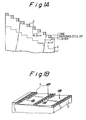
- Al atoms diffuse on the surface of the buffer layer 2 and adhere preferentially to a step edge to grow in a lateral direction thereon, and As atoms adhere onto the Al atoms to form monomolecule layers 3, as shown in Figs. 1A and 1B.
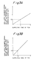
- AlAs layer thickness monomolecular unit grown on a JUST-CUT (100) GaAs substrate and a TEA gas supplying duration, as shown in Fig. 3A.
- the JUST-CUT substrate is a nonoriented substrate, e.g., (100) GaAs substrate.
- a pulse feeding duration t1 corresponding to a half of the terrace width formation of the AlAs layer on the step terrace is predetermined to form the AlAs monomolecular layer 3 in the lateral direction to the half distance (8.1 nm) of the terrace width (16.2 nm), as shown in Fig. 1A.
- the flow of the TEA gas is stopped and the TEG is supplied.
- Ga atoms diffuse on the remaining exposed area of the buffer layer 2 and adhere preferentially to a step side of the grown AlAs layer to grow in a lateral direction thereon, and As atoms adhere onto the Ga atoms to form monomolecule layers 4, as shown in Figs. 1C and 1D.
- a GaAs layer thickness monomolecular unit grown on a JUST GaAs substrate and a TEG gas supplying duration, as shown in Fig. 3B.
- a pulse supplying duration t2 corresponding to a half terrace width formation of the GaAs layer on the step terrace is predetermined to form the GaAs monomolecular layer 4 in the lateral direction to the rest of the terrace width, as shown in Fig. 1C.
- GaAs/AlAs superlattice 5 consisting of the AlAs layers 3 and GaAs layers 4 which extend in a vertical direction and are periodically arranged in a lateral (horizontal) direction, as shown in Fig. 1E.
- the GaAs layer grows either to extend over the atomic step (terrace) width and on the AlAs layer formed on the neighboring lower step or two leave an uncovered portion of the terrace. Therefore, the formed vertical type superlattice, in practice, has a structure in which the interfaces of the AlAs layers 3 and GaAs layers 4 are inclined to the substrate 1 and are not flat, as shown in Fig. 1E. For example, if a number of the atoms arranged on the terrace per growth cycle is over by one atom, the interfaces may be inclined at 45°. It is difficult to use the vertical type superlattice having the inclined and nonflat interfaces for quantum effect devices (a quantum interference effect transistor or the like) which are expected to come into practical use.
- quantum effect devices a quantum interference effect transistor or the like
- An object of the present invention is to provide a method of forming a compound semiconductor vertical type superlattice layer provided with interfaces of first semiconductor thin layers and second semiconductor thin layers interfaces of which are vertical to the substrate surface and are improved with respect to flatness.
- Another object of the present invention is to provide an improved compound semiconductor vertical type superlattice suitable for semiconductor devices.
- a method of forming a vertical type superlattice layer of first compound semiconductor AC thin layers and second compound semiconductor BC thin layers comprising the step of repeating the following process steps (a), (b) and (c): the process step (a) supplying a first source gas containing the element A to grow a single atomic A layer from the side of the atomic step in a lateral direction and on a portion (particularly, a half) of the atomic step width under a growing time control; the process step (b) supplying a second source gas containing the element B, under a self-limiting condition, to form a single atomic B layer on the rest of the step width; and the process step (c) supplying a third source gas containing the
- a supplying system (sequence) of source gases containing elements A, B, and C and growth conditions are controlled, to grow a single atomic layer A on a portion of an atomic step of the substrate, to grow a single atomic layer B on the rest under a self-limiting mechanism for preventing the thickness thereof from increasing (at this duration, the element (atoms) B deposits on the step only and does not deposit on the single atomic layer A on the neighboring lower atomic step), and then the element (atoms) C is deposited on the single atomic layers A and B, so as to form the monomolecular layers AC and BC, respectively.
- the monomolecular layer BC does not extend over the step (terrace) width and is not short for filling the remaining portion with the result that one of the interfaces of the monomolecular layer BC with the monomolecular layer AC is made flat and vertical to the substrate.
- the atomic step surface is formed by epitaxially growing a buffer compound semiconductor layer on the single crystal compound semiconductor substrate having a vicinal surface.
- a compound semiconductor superlattice layer consisting of a first compound semiconductor AC and a second compound semiconductor BC is formed in accordance with the basic method of the present invention as follows:
- a vicinal compound semiconductor substrate (misoriented substrate) 1 with atomic step stairs (steps and terraces) is prepared in a conventional manner.
- the substrate 1 has a slightly misoriented crystalline surface as the atomic stair steps of which steps have a step height being not necessarily a single atomic layer height and have a nonuniform terrace width.
- a buffer layer 2 of a compound semiconductor having the same lattice constant as that of the substrate 1 is epitaxially grown on the substrate 1 by an MOCVD method or a gas source MBE method with the result that its surface consists of uniform atomic steps having the step height equal to a monomolecular height, and a uniform terrace width.
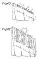
- a first source gas containing an element (atoms) A for the first compound semiconductor AC is pulsatively supplied under a growth condition that a surface diffusion length (distance) of the atoms A is larger than the step width (a step-flow growth mode), as shown in Fig. 4B, the atoms A preferentially adhere to each of the step edges and on the terrace (step) surface to grow each single atomic layer 11 in a lateral direction.
- the growth of the layer 11 is controlled essentially by using a relationship (indicated with a solid line or a broken line, as shown in Fig.
- the gas feeding duration is predetermined as "t1" corresponding to a half of the single atomic layer thickness (regarded as a half of the terrace width), so as to grow the layer 11 on the half of the step (terrace) width.
- the relationship indicated with the broken curve line is regarded as a self-limiting condition explained hereinafter.
- a second source gas containing an element B for the second compound semiconductor BC is pulsatively supplied under a self-limiting growth condition, as shown in Fig. 4C, a single atomic layer 12 is grown on the rest (half) of the terrace (on the exposed buffer layer portion: C atoms appear on the surface).
- the growth of the layer 12 is automatically stopped, because there is a self-limiting mechanism (i.e., a saturation condition) of the growth of the element B layer on a JUST substrate, as shown in Fig. 5B.
- the atoms B are also not deposited (or absorbed) on the now formed layer 12 and also on the previous formed element A layer 11.
- a metalorganic gas of the second source gas containing element B is not decomposed on the layer 11 to prevent the atoms B from being deposited thereon.
- a third source gas containing an element C for both the compound semiconductors AC and BC is also pulsatively supplied under the self-limiting growth condition, as shown in Fig. 4D, and the atoms C are deposited to grow a single atomic layer 13 on the layer 11 and 12.
- the layer 13 combines with the atomic layers 11 and 12 to form a monomolecular AC layer 14 and a monomolecular BC layer 15, as shown in Fig. 4D.
- the feeding of the third source gas is then stopped.
- the above-mentioned gas supplying (deposition or growth) steps for the single atomic layers 11, 12 and 13 are periodically repeated to grow the first compound semiconductor AC layers 14 and second compound semiconductor BC layers 15 in a vertical direction, as shown in Fig. 4E, which layers 14 and 15 are alternately arranged in a lateral (transverse) direction to form a vertical type AC/BC superlattice layer 16.
- Fig. 4E one of the both AC/BC interfaces (a right-hand interface in Fig. 4E) of each of the BC layers 15 becomes flat and vertical, which prevents the whole interfaces from inclining and thus the oblique growth of the superlattice layer is as shown in Fig. 1E.
- Fig. 1E Furthermore, in Fig.
- each of the atomic steps of the stairs has a monomolecular layer height (which is far smaller as compared with the terrace width), so that the substrate with the formed superlattice layer 16 can be observed, as shown in Fig. 7.
- the elements A and B are atoms of group III, group II or group VI of a periodic table, and the element C is an atom of group V, group VI or group II. It is preferable that the group II element is zinc (Zn), the group III elements are aluminum (Al), gallium (Ga) and indium (In), the group V elements are arsenic (As) and phosphorus (P), and the group VI elements are selenium (Se), sulfur (S) and tellurium (Te).
- the superlattice layer on the suitable substrate, such as AlAs/GaAs superlattice on GaAs substrate, ZnSe/ZnS superlattice on GaAs substrate, InAs/GaAs superlattice on InP substrate, and ZnSe/ZnTe superlattice on InP substrate.
- the obtained substrate with the vertical type superlattice layer formed in accordance with the present invention is used for semiconductor devices, such as a field-effect transistor (disclosed in K. TSUBAKI et al.: “New Field-Effect Transistor with Quantum Wire and Modulation-doped Heterostructures", Electronics Letters, 29th September, 1988, Vol. 24, No. 20, pp. 1267-1268 and K. TSUBAKI et al.: “Low Dimensional Electron Gas Field Effect Transistor Using Fractional Layer Superlattice", Extended Abstructs (The 49th, Autamn Meeting, 1988), The Japan Society of Applied Physics, 5a-C-11. p. 966), an electron mobility modulating transistor (disclosed in Y.
- a field-effect transistor disclosed in K. TSUBAKI et al.: "New Field-Effect Transistor with Quantum Wire and Modulation-doped Heterostructures", Electronics Letters, 29th September, 1988, Vol.
- An AlAs/GaAs vertical type superlattice layer is formed on a GaAs single crystal substrate by using an MOCVD process in the following manner.
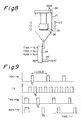
- a conventional vertical MOCVD apparatus shown in Fig. 8 is used.
- the apparatus comprises a reactor 21, a holder 22, an induction heating coil 23, a manifold 24 and vent pipes 24 and 25.
- the holder 22 holds a vicinal GaAs substrate 26 and heat it to a predetermined (growth) temperature.
- the vent pipes 24 and 25 are connected to a vacuum pump (not shown).
- the manifold 24 is provided with inlet pipes for supplying (1) a tri-methylaluminum (TMA) gas and a hydrogen (H2) carrier gas, (2) a tri-methylgallium (TMG) gas and a H2 carrier gas, (3) an AsH3 gas and a H2 carrier gas and (4) a purge H2 carrier gas.
- TMA tri-methylaluminum
- H2 hydrogen
- TMG tri-methylgallium
- Each of the pipes has a mass flow controller and a switching valve for accurately supplying the gas therethrough.
- a vicinal (100) GaAs substrate (wafer) 26 having a vicinal angle ⁇ of 1° is prepared by cutting a single crystal GaAs ingot, polishing, chemicaletching and setting it on the holder 22 within the reactor 21.
- the reactor 21 is evacuated to a vacuum pressure of 10 ⁇ 1 Torr (13 Pa) or less by a suitable vacuum pump.
- the substrate 26 is heated and maintained at a predetermined temperature of from 300 to 600°C, e.g., 450°C.
- the TMG gas (and H2 gas) and the AsH3 gas (and H2 gas) are simultaneously supplied (Fig. 9) into the reactor 21 though the manifold 24 to epitaxially grow a GaAs buffer layer 2 at the inside vacuum pressure of 20 Torr (2600 Pa) or less, as shown in Fig. 4A.
- the GaAs buffer layer 2 has atomic step stairs having one monomolecular layer height per step and uniform terrace (step) width (e.g., 16.2 nm).
- the purge H2 gas is supplied into the reactor 21 for a duration T4 , e.g., 1 second to purge away the TMG and AsH3.
- the TMA gas (and H2 gas), TMG gas (and H2 gas), the AsH3 gas (and H2 gas) and the purge H2 carrier gas are pulsatively fed supplied durations T1, T2 , T3 and T4 , respectively.
- the mixture gas of the TMA gas and the H2 gas (40 sccm of TMA gas) is supplied at a flow rate of from 10 to 60 sccm (e.g., 40 sccm) and the substrate 1 is maintained at 400 to 530 °JC (e.g., 450°C)
- Al atoms decomposed from the TMA preferentially adhere to step edges and on the terraces to grow single atomic layers 11 in a lateral direction under the step-flow condition, as shown in Fig. 4B.
- the supplying duration T1 (e.g., 1 second) of the TMA gas per pulse is set to make the growth distance of the Al single crystal layer (monoatomic layer) 11 just half of the step terrace width, as shown in Fig. 5A.
- the purge H2 gas is also supplied into the reactor 21 for, e.g., 1 second to purge away the TMA.
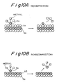
- the TMG on the As atoms of the exposed remaining surface of the terrace can decompose to deposit Ga atoms thereon, as shown in Fig. 10A, to grow single atomic layers 12 covering the remaining terrace, as shown in Fig. 4C, under suitable conditions.
- the TMG on the Al atoms of the formed atomic layer 11 does not decompose, so that the Al atoms combined with the methyl are not deposited, as shown in Fig. 10B.
- the growth conditions (growth temperature, gas flow rate or the like) of the layers 12 are determined to attain a self-limiting condition, as shown in Fig. 5B.
- the substrate temperature (i.e., the growth temperature) and the gas flow rate are decided at the above-mentioned values.
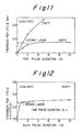
- the self-limiting phenomenon of a Ga atomic layer formation appears, as shown in Fig. 11, under the following conditions.
- Substrate (100) GaAs JUST substrate Growth temperature: 450°C, 500°C (comparative example)
- Flow rate of TMG containing gas TMG gas (40 sccm) and H2 gas Gas supplying duration per pulse: 1, 2, 5 and 10 seconds
- Vacuum pressure 20 Torr (3-10 Seconds)
- the curved line at 450°C proves that the growing effect is saturated to one atomic layer thickness.
- the self-limiting mechanism does not appear.
- the purge H2 gas is also supplied into the reactor 21 for, e.g., 1 second to purge away the TMG, as shown in Fig. 9.
- an AsH3 gas (10%) diluted with the H2 gas is fed at a flow rate of from 300 to 600 sccm (e.g., 480 sccm) and the substrate 1 is maintained at 400 to 500°C (e.g., 450°C), the As atoms deposited on the single atomic layers 11 and 12 to form single atomic layer 13, as shown in Fig. 4D, under the self-limiting condition.
- the As atoms chemically react with the Al atoms and the Ga atoms to form monomolecular AlAs layer 14 and monomolecular GaAs layers 14.
- the right side of the GaAs layer 13 exactly corresponds to the right side of the atomic step terrace.
- the curved line at 500°C proves that the growing effect is saturated to slightly in excess of one atomic layer thickness.
- the above-mentioned gas supplying (deposition or growth) steps for the single atomic layers 11, 12 and 13 are repeated (e.g., 1000 cycles) in accordance with the gas supplying sequence of Fig. 9 to grow the AlAs layers 14 and the GaAs layers 15 in a vertical direction whereby the GaAs/AlAs superlattice layer 16 (having a thickness of 250 nm) is formed, as shown in Fig. 4E.
- An AlAs/GaAS vertical type superlattice layer is formed on a GaAs single crystal substrate by using a gas source MBE (MOMBE) process in the following manner.
- MOMBE gas source MBE
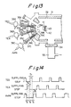
- a conventional gas source MBE apparatus shown in Fig. 13 is used.
- the apparatus comprises a chamber 31 with a cooling (liquid nitrogen) shroud (wall) 32, a vacuum pump 33 connected to the chamber 31 through a gate valve 34, and three source gas feeders 35A, 35B and 35C.
- the gas feeders 35A, 35B and 35C are provided with switching valves 36A, 36B and 36C, inlet pipes 37A, 37B and 37C, and heaters 38A, 38B and 38C, and are connected to a TEG gas source, a TEA gas source and a AsH3 gas source, respectively.
- the heaters 38A and 38B heat the inlet pipes 37A and 37B to 80-150°C to prevent the condensation of the metalorganic gases.
- the chamber 31 has a holder 42 with a heater 43 and shutters 39A, 39B and 39C arranged between the holder 42 and the inlet pipes 37A, 37B and 37C, respectively. Feeding and nonfeeding (Stop) of the source gases are accurately controlled by controlling the switching valves 36A, 36B and 36C and shutters 39A, 39B and 39C. When the gas is not supplied into the chamber 31, it is discharged to an exhaust line from the switching valves 36A, 36B and 36C, so that an rapid switching of the gas is attained.
- the AsH3 gas is cracked by heating it to about 1100°C with the heater 38C to feed As2 into the chamber 31.
- a vicinal (100)GaAs substrate (wafer) 41 having a vicinal angle ⁇ of 1° prepared for Example 1 is used and is set on the holder 42 within the chamber 31.
- the chamber 31 is evacuated to a vacuum pressure of 10 ⁇ 9 to 10 ⁇ 9 Torr by the vacuum pump 33.
- the substrate 41 is heated by the heater 43 and maintained at a predetermined temperature of from 300 to 650°C, e.g., 580°C.
- the TMG gas and the AsH3 gas are simultaneously supplied (Fig. 14) into the chamber 31 though the opened shutters 39A and 39C to epitaxially grow a GaAs buffer layer 2 at the inside vacuum pressure of 10 ⁇ 5 to 1.5 x 10 ⁇ 4 Torr (e.g., 5 x 10 ⁇ 5 Torr), as shown in Fig. 4A.
- the GaAs buffer layer 2 has atomic step stairs having one monomolecular layer height per step and uniform terrace (step) width (e.g., 16.2 nm) similar to Example 1.
- the supplying of the gases is stopped for a duration T5 , e.g., 0.5 seconds to remove residual gases.
- the TEA gas, TEG gas and the AsH3 gas are pulsatively fed for durations T6 , T7 and T8 at regular intervals (interruption durations) T5.
- the TEA gas is fed at a flow rate of from 0.3 to 0.8 sccm (e.g., 0.5 sccm) and the substrate 1 is maintained at 300 to 600°C (e.g., 400°C)
- Al atoms decomposed from the TEA preferentially adhere to step edges and on the terraces to grow single atomic layers 11 in a lateral direction under the step-flow condition, as shown in Fig. 4B.
- the supplying duration T6 (e.g., 1 second) of the TEA gas per pulse is set to make the growth distance of the Al single crystal layer (monoatomic layer) 11 just half of the step terrace width, as shown in Fig. 5A.
- the half of the terrace is covered with the Al atomic layer 11.
- the TEA gas is not supplied into the chamber 31 for, e.g., 0.5 seconds to take away the TEA.
- the TEG on the As atoms of the exposed surface of the terrace can decompose to deposit Ga atoms thereon to grow single atomic layers 12 covering the remaining terrace, as shown in Fig. 4C.
- the TEG on the Al atoms of the formed atomic layer 11 does not decompose, so that the Al atoms combined with the ethyl radical are not deposited.
- the growth conditions (growth temperature, gas flow rate or the like) of the layers 12 are determined to attain a self-limiting condition, as shown in Fig. 5B.
- the substrate temperature (i.e., the growth temperature) and the gas flow rate are decided at the above-mentioned value.
- the TEG gas is not supplied into the chamber 31 for, e.g., 0.5 seconds to take away the TEG.
- the AsH3 gas is supplied at a flow rate of from 1 to 8 sccm (e.g., 2 sccm) and the substrate 1 is maintained at 300 to 480°C (e.g., 400°C) for the duration T8 of 1 to 10 seconds (e.g., 2 seconds), the As atoms deposited on the single atomic layers 11 and 12 to form single atomic layer 13, as shown in Fig. 4D, under the self-limiting condition.
- the As atoms chemically react with the Al atoms and the Ga atoms to form monomolecular AlAs layer 14 and monomolecular GaAs layers 14.
- the right side of the GaAs layer 13 exactly corresponds to the right side of the atomic step terrace.
- the obtained substrate with improved vertical type superlattice layer is used in a production of, e.g., a field-effect (FET) transistor in the following manner.
- FET field-effect
- An n+-type (Si-doped) AlGaAs layer is epitaxially grown on the superlattice layer.
- a source electrode and a drain electrode are selectively formed on the AlGaAs layer and by a vapor deposition process and are alloyed with portions of the AlGaAs layer, the supper lattice layer, the buffer layer and the substrate to form a source region and a drain region.
- a gate electrode is formed on the AlGaAs layer between the source and drain electrodes to produce the FET transistor.
Applications Claiming Priority (1)
| Application Number | Priority Date | Filing Date | Title |
|---|---|---|---|
| JP1228287A JPH0391922A (ja) | 1989-09-05 | 1989-09-05 | 化合物半導体の縦型超格子の形成方法 |
Publications (2)
| Publication Number | Publication Date |
|---|---|
| EP0421608A2 true EP0421608A2 (de) | 1991-04-10 |
| EP0421608A3 EP0421608A3 (en) | 1991-07-10 |
Family
ID=16874107
Family Applications (1)
| Application Number | Title | Priority Date | Filing Date |
|---|---|---|---|
| EP19900309635 Withdrawn EP0421608A3 (en) | 1989-09-05 | 1990-09-04 | Method of forming a vertical type superlattice layer of compound semiconductor |
Country Status (2)
| Country | Link |
|---|---|
| EP (1) | EP0421608A3 (de) |
| JP (1) | JPH0391922A (de) |
Cited By (3)
| Publication number | Priority date | Publication date | Assignee | Title |
|---|---|---|---|---|
| EP2527500A4 (de) * | 2010-01-20 | 2014-04-09 | Jx Nippon Mining & Metals Corp | Verfahren zur herstellung eines epitaktischen kristallsubstrats |
| CN111063750A (zh) * | 2019-12-10 | 2020-04-24 | 广东省半导体产业技术研究院 | 一种紫外光电器件及其制备方法 |
| CN111934200A (zh) * | 2020-08-20 | 2020-11-13 | 湖南科莱特光电有限公司 | 垂直型III-V族超晶格材料、具有超晶格分布的InGaAsSb四元合金及制备方法 |
Families Citing this family (1)
| Publication number | Priority date | Publication date | Assignee | Title |
|---|---|---|---|---|
| FI119277B (fi) | 2003-11-21 | 2008-09-30 | Polar Electro Oy | Järjestely, menetelmä ja tietokoneohjelma ihmisen fyysisen aktiivisuustason määrittämiseksi |
Family Cites Families (1)
| Publication number | Priority date | Publication date | Assignee | Title |
|---|---|---|---|---|
| JPS6459808A (en) * | 1987-08-31 | 1989-03-07 | Nec Corp | Growth of semiconductor |
-
1989
- 1989-09-05 JP JP1228287A patent/JPH0391922A/ja active Pending
-
1990
- 1990-09-04 EP EP19900309635 patent/EP0421608A3/en not_active Withdrawn
Cited By (5)
| Publication number | Priority date | Publication date | Assignee | Title |
|---|---|---|---|---|
| EP2527500A4 (de) * | 2010-01-20 | 2014-04-09 | Jx Nippon Mining & Metals Corp | Verfahren zur herstellung eines epitaktischen kristallsubstrats |
| CN111063750A (zh) * | 2019-12-10 | 2020-04-24 | 广东省半导体产业技术研究院 | 一种紫外光电器件及其制备方法 |
| CN111063750B (zh) * | 2019-12-10 | 2021-07-27 | 广东省半导体产业技术研究院 | 一种紫外光电器件及其制备方法 |
| CN111934200A (zh) * | 2020-08-20 | 2020-11-13 | 湖南科莱特光电有限公司 | 垂直型III-V族超晶格材料、具有超晶格分布的InGaAsSb四元合金及制备方法 |
| CN111934200B (zh) * | 2020-08-20 | 2021-10-15 | 湖南科莱特光电有限公司 | 垂直型III-V族超晶格材料、具有超晶格分布的InGaAsSb四元合金及制备方法 |
Also Published As
| Publication number | Publication date |
|---|---|
| JPH0391922A (ja) | 1991-04-17 |
| EP0421608A3 (en) | 1991-07-10 |
Similar Documents
| Publication | Publication Date | Title |
|---|---|---|
| Sumiya et al. | Growth mode and surface morphology of a GaN film deposited along the N-face polar direction on c-plane sapphire substrate | |
| US8482104B2 (en) | Method for growth of indium-containing nitride films | |
| US5679152A (en) | Method of making a single crystals Ga*N article | |
| US7982208B2 (en) | Non-polar (Al,B,In,Ga)N quantum well and heterostructure materials and devices | |
| EP0340113B1 (de) | Verfahren zum Aufwachsen einer Galliumarsenid-Schicht auf einem Silizium-Substrat | |
| Karam et al. | Growth of device quality GaN at 550 C by atomic layer epitaxy | |
| KR102075177B1 (ko) | 에피택시 기판, 에피택시 기판의 제조 방법 및 에피택시 기판을 구비한 광전 반도체 칩 | |
| KR100692267B1 (ko) | Ⅲ족 질화물 반도체 결정의 제조 방법 | |
| US11843072B2 (en) | Light emitting diodes with n-polarity and associated methods of manufacturing | |
| JP4356208B2 (ja) | 窒化物半導体の気相成長方法 | |
| EP1038056B1 (de) | Verfahren zur züchtung einer pufferschicht durch molekularstrahlenepitaxie | |
| WO2002017369A1 (en) | Method of fabricating group-iii nitride semiconductor crystal, metho of fabricating gallium nitride-based compound semiconductor, gallium nitride-based compound semiconductor, gallium nitride-based compound semiconductor light-emitting device, and light source using the semiconductor light-emitting device | |
| US7504321B2 (en) | MBE growth of an algan layer or AlGaN multilayer structure | |
| US6894323B2 (en) | Group III nitride semiconductor device and its method of manufacture | |
| US7648577B2 (en) | MBE growth of p-type nitride semiconductor materials | |
| CN115116828A (zh) | 基于氮化物单晶衬底的同质外延结构及其均匀性调控方法 | |
| Zhou et al. | Growth of GaN films by combined laser and microwave plasma enhanced chemical vapour deposition | |
| KR960004591B1 (ko) | 도우프된 결정 성장 방법 | |
| EP3799110A1 (de) | Gruppe-iii-nitrid-halbleitersubstrat und herstellungsverfahren dafür | |
| JP3112445B2 (ja) | 窒化ガリウム系化合物半導体の気相成長装置 | |
| JPH0391922A (ja) | 化合物半導体の縦型超格子の形成方法 | |
| JPH078756B2 (ja) | 化合物半導体薄膜形成法 | |
| JPH0620043B2 (ja) | ▲iii▼−▲v▼族化合物半導体結晶のド−ピング方法 | |
| JPH0888185A (ja) | 半導体結晶成長方法 | |
| JPH04238889A (ja) | 化合物半導体の結晶成長方法 |
Legal Events
| Date | Code | Title | Description |
|---|---|---|---|
| PUAI | Public reference made under article 153(3) epc to a published international application that has entered the european phase |
Free format text: ORIGINAL CODE: 0009012 |
|
| AK | Designated contracting states |
Kind code of ref document: A2 Designated state(s): DE FR GB |
|
| PUAL | Search report despatched |
Free format text: ORIGINAL CODE: 0009013 |
|
| AK | Designated contracting states |
Kind code of ref document: A3 Designated state(s): DE FR GB |
|
| STAA | Information on the status of an ep patent application or granted ep patent |
Free format text: STATUS: THE APPLICATION IS DEEMED TO BE WITHDRAWN |
|
| 18D | Application deemed to be withdrawn |
Effective date: 19920111 |