EP0421332A2 - Appareil de commande de charge pour véhicules - Google Patents
Appareil de commande de charge pour véhicules Download PDFInfo
- Publication number
- EP0421332A2 EP0421332A2 EP90118827A EP90118827A EP0421332A2 EP 0421332 A2 EP0421332 A2 EP 0421332A2 EP 90118827 A EP90118827 A EP 90118827A EP 90118827 A EP90118827 A EP 90118827A EP 0421332 A2 EP0421332 A2 EP 0421332A2
- Authority
- EP
- European Patent Office
- Prior art keywords
- value
- output
- control value
- circuit
- duty factor
- Prior art date
- Legal status (The legal status is an assumption and is not a legal conclusion. Google has not performed a legal analysis and makes no representation as to the accuracy of the status listed.)
- Granted
Links
Images


Classifications
-
- H—ELECTRICITY
- H02—GENERATION; CONVERSION OR DISTRIBUTION OF ELECTRIC POWER
- H02J—CIRCUIT ARRANGEMENTS OR SYSTEMS FOR SUPPLYING OR DISTRIBUTING ELECTRIC POWER; SYSTEMS FOR STORING ELECTRIC ENERGY
- H02J7/00—Circuit arrangements for charging or depolarising batteries or for supplying loads from batteries
- H02J7/14—Circuit arrangements for charging or depolarising batteries or for supplying loads from batteries for charging batteries from dynamo-electric generators driven at varying speed, e.g. on vehicle
- H02J7/16—Regulation of the charging current or voltage by variation of field
- H02J7/24—Regulation of the charging current or voltage by variation of field using discharge tubes or semiconductor devices
- H02J7/2434—Regulation of the charging current or voltage by variation of field using discharge tubes or semiconductor devices with pulse modulation
-
- Y—GENERAL TAGGING OF NEW TECHNOLOGICAL DEVELOPMENTS; GENERAL TAGGING OF CROSS-SECTIONAL TECHNOLOGIES SPANNING OVER SEVERAL SECTIONS OF THE IPC; TECHNICAL SUBJECTS COVERED BY FORMER USPC CROSS-REFERENCE ART COLLECTIONS [XRACs] AND DIGESTS
- Y02—TECHNOLOGIES OR APPLICATIONS FOR MITIGATION OR ADAPTATION AGAINST CLIMATE CHANGE
- Y02T—CLIMATE CHANGE MITIGATION TECHNOLOGIES RELATED TO TRANSPORTATION
- Y02T10/00—Road transport of goods or passengers
- Y02T10/80—Technologies aiming to reduce greenhouse gasses emissions common to all road transportation technologies
- Y02T10/92—Energy efficient charging or discharging systems for batteries, ultracapacitors, supercapacitors or double-layer capacitors specially adapted for vehicles
Definitions
- the present invention relates to a charging control apparatus for a vehicle for controlling the power generation of a generator to charge a battery for a vehicle and, more particularly, to a charging control apparatus which controls a rate of increase of a field current of the generator when an electric load was applied to the generator.
- JP-A-62-64299 wherein a battery voltage and a predetermined voltage are compared and when the battery voltage is lower than the predetermined voltage, an up/down counter is incremented and, contrarily, when the battery voltage is higher than the predetermined voltage, the up/down counter is decremented.
- the up/down counter by extending a period to increment the up/down counter, even if a battery voltage suddenly decreases by applying an electric load, the up/down counter is gradually increased, so that a field current is gradually increased as shown in Fig. 9. Therefore, the electric load is also slowly applied to an engine and an inconvenience such as an engine stall or the like can be prevented.
- the above conventional charging apparatus has a short coming as described below.
- an object of the present invention to certainly prevent that a generator adversely influences an engine when an electric load is applied.
- a charging control apparatus of an alternating generator for a vehicle driven by an engine having a stator winding and a field winding, and charging a battery
- the apparatus comprises: switching means connected in series to the field winding; comparing means for detecting a voltage of the battery and comparing the battery voltage and a sawtooth wave of a predetermined period; memory means for storing a value regarding a duty factor of an output of the comparing means at the predetermined period; control value increasing/decreasing means for comparing the value regarding the duty factor obtained from the memory means with a duty factor of a control value, for increasing the duty factor of the control value at the predetermined period when the duty factor of the control value is smaller than the value regarding the duty factor obtained from the memory means, and for decreasing the duty factor of the control value when the duty factor of the control value is larger than the value regarding the duty factor obtained from the memory means; and AND means for calculating an AND between a value corresponding to the outputted control value from the control value increasing/de
- the duty factor can be gradually increased from the present value of the duty factor. Thus, it is prevented that a sudden load fluctuation is applied to the engine.
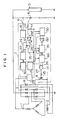
- an AC generator for a vehicle comprises: a Y-connected three-phase armature winding 1 which is a stator winding; a field winding 2 which is rotated by an engine (not shown); and a rectifier 3 to full-wave rectify an AC output of the armature winding 1.
- the generator is driven by the engine through a belt and a pulley in a well-known manner.
- Reference numeral 4 denotes a battery
- 5 indicates an electric load connected to the battery 4 and 6 an ignition switch.
- a control circuit 7 controls a field current flowing in the field winding 2 of the generator and is assembled in an AC generator for a vehicle as disclosed in, for instance, U.S. Patent Serial No. 353,861.
- control circuit 7 will now be described in detail.
- the current flowing through the field winding 2 is controlled by a field effect transistor (MOSFET) 8 as switching means.
- MOSFET field effect transistor
- a flywheel diode 9 is connected to the field winding 2.
- Reference numeral 12 denotes a differential amplifier.
- a (+) terminal of the amplifier 12 is connected to a node between a first resistor 10 connected to the battery 4 and a second resistor 11, while a reference voltage V ref is input to a (-) terminal.
- the differential amplifier 12 outputs a Hi level signal when a voltage of battery 4 is equal to or higher than a predetermined value (e.g., 14 V).
- Reference numeral 13 denotes a comparator.
- An output of a sawtooth wave generating circuit 40 which will be explained hereinlater, is inputted to a (+) terminal and an output of the differential amplifier 12 is inputted to a (-) terminal, respectively.
- Reference numeral 14 denotes an AND circuit. An output of the comparator 13 and an output of a pulse width converting circuit 80, which will be explained hereinlater, are inputted to the AND circuit 14. An output of the AND circuit 14 is inputted to a gate of the MOSFET 8 through a third resistor 15.
- Reference numeral 16 denotes a power supply circuit to generate a power source for making each circuit in the control circuit 7 operative and a reference voltage from a battery voltage which is supplied via the IG switch 6.
- Reference numeral 17 denotes a reference oscillating circuit which outputs a signal at a period of 4 [ ⁇ sec].
- Reference numeral 30 denotes a frequency dividing circuit to obtain a signal of a desired oscillating period which is derived by frequency dividing a reference oscillating signal of the reference oscillating circuit 17.
- the frequency dividing circuit is shown in detail in Fig. 3.
- Reference numeral 301 denotes a counter and 302 indicates a clock input terminal which is connected to an output terminal of the reference oscillating circuit 17.
- Reference numerals 303 to 317 denote output terminals of the counter.
- the waveforms obtained by frequency dividing the clock input from the reference oscillating circuit 17 into 1/1 to 1/15 are inputted to the output terminals 303 to 317.
- Reference numeral 40 denotes the sawtooth wave generating circuit to generate a voltage waveform like a sawtooth wave from the signal from the frequency dividing circuit by the D/A conversion.
- the sawtooth wave generating circuit 40 is shown in detail in Fig. 4.
- a regulated voltage which is obtained from the power supply circuit 16 is supplied to a terminal 425.
- Reference numerals 401 to 405 denote constant current circuits and 411 to 415 indicate switches for turning on and off currents which are supplied from the constant current circuits to rudder resistors 416 to 424.
- Terminals 406 to 410 of the switches 411 to 415 are connected to the output terminals 308 to 313 of the frequency dividing circuit 30 shown in Fig. 3, respectively.
- the signals from the frequency dividing circuit 30 are sequentially inputted the terminals 406 to 410, the switches 411 to 415 are sequentially turned on, and currents flow through the resistors 416 to 424.
- the voltage is sequentially reduced and a sawtooth waveform of the period of 4 [msec] is outputted to a terminal 426 as shown in Fig. 2.
- the terminal 426 is connected to the (+) terminal of the comparator 13 shown in Fig. 1.
- an A/D converting circuit 50 By detecting the timing of the output signal of the comparator 13, an A/D converting circuit 50 detects a duty factor of an exciting signal to the field winding 2 which is necessary to control the battery voltage to the set voltage, and converts the detected duty factor into the digital signal.
- Reference numeral 60 denotes a magnitude comparator for comparing an output signal of the A/D converting circuit with a value from up/down counter, which will be explained hereinlater.
- Reference numeral 70 denotes the up/down counter serving as control value increasing/decreasing means for executing an UP (increment) or DOWN (decrement) operation on the basis of an output signal of the magnitude comparator.
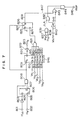
- the A/D converting circuit 50, magnitude comparator 60, and up/down counter 70 will now be described in detail with reference to Fig. 5.
- Output terminals H7 to H10 of the frequency dividing circuit 30 are connected to terminals 501 to 504.
- the output terminals 501 to 504 are connected to D1 to D4 terminals 565 to 568 of a D type flip-flop 514 and are also inputted to a 4-input AND circuit 508.
- An output signal of the 4-innut AND circuit 508 is connected to a D input terminal of a D type flip-flop 509 and is also connected to an input terminal of an inverter 510.
- An output H6 of the frequency dividing circuit is connected to a clock input terminal 506 of the D type flip-flop 509.
- An inverted output Q of the flip-flop 509 is inputted to an NAND circuit 511.
- an output 25 of the comparator 13 is connected to a terminal 507 and to an input terminal of the NAND circuit 511.
- An output terminal of the inverter 510 and an output terminal of the NAND circuit 511 are connected to an input terminal of an AND circuit 512.
- An output terminal of the AND circuit 512 is connected to a clock input terminal 570 of the 4-input D type flip-flop 514.
- Q1 to Q4 outputs 516 to 519 of the flip-flop 514 are inputted to input terminals A0 to A3 (520 to 523) of a magnitude comparator 50 (515).
- the value which was obtained by A/D converting a duty signal of the MOSFET 8 is outputted to the Q1 to Q4 output terminals 516 to 519 of the flip-flop 514.
- the comparison signal 25 obtained by comparing a sawtooth wave 24 of the sawtooth wave generating circuit 40 with an output 28 of the differential amplifier 12 by the comparator 13 is inputted to the terminal 507.
- a Hi signal is inputted to the clock input terminal 570 of the flip-flop 514.
- the signals which are inputted to the D1 to D4 input terminals 565 to 568 are set to the Q1 to Q4 output terminals of the flip-flop 514. Since the signals which are inputted to the the D1 to D4 input terminals are the outputs of the frequency dividing circuit 30, a period of time from an A point corresponding to the leading edge of the sawtooth wave shown in Fig. 2 to the B point is expressed.
- Q2 to Q5 output terminals 547 to 550 of an up/down counter 545 are connected to B0 to B3 output terminals 526 to 529 of the magnitude comparator 515.
- the magnitude comparator 515 compares the binary signals of the A0 to A3 input terminals 520 to 523 with the binary signals of the B0 to B3 output terminals 526 to 529.
- a ⁇ B an H level signal is outputted from a terminal 553.
- a ⁇ B an L level signal is outputted from the terminal 553.
- the output signal of the terminal 553 is connected to a D input terminal 554 of a D type flip-flop 525.
- the output signal H10 of the frequency dividing circuit 30 is outputted to a clock input terminal 569 of the D type flip-flop 525.
- a Q output 556 of the flip-flop 525 is connected to an input terminal of a 3-input NAND circuit 544 and a Q output 555 is connected to an input terminal of a 3-input NAND circuit 543.
- a selector circuit is constructed by AND circuits 535, 537, 538, and 540, inverters 536 and 539, and OR circuits 541 and 542.
- the output H10 of the frequency dividing circuit 30 is selected as an output 571 of the OR circuit 541 and, similarly, the output H10 of the frequency dividing circuit 30 is also selected as an output 572 of the OR circuit 542.
- an output H15 of the frequency dividing circuit 30 is selected as an output 571 and an output H13 of the frequency dividing circuit 30 is selected as an output 572.
- the output 571 is connected to an input terminal of the 3-input NAND circuit 543.
- the output 572 is connected to an input terminal of the 3-input NAND circuit 544.
- An L level signal is outputted from the terminal 530 when a rotational speed detecting circuit 23, which will be explained hereinlater, detects that the engine rotational speed is equal to or less than 3000 [rpm].
- An output 551 of the 3-input NAND circuit 543 is connected to an UP input terminal of the up/down counter 545.
- An output 552 of the 3-input NAND circuit 544 is connected to a DOWN input terminal of the up/down counter 545.
- the Q1 to Q3 outputs 546 to 550 of the up/down counter 545 are inputted to both of a 5-input NAND circuit 557 and a 5-input OR circuit 558.
- Outputs of the NAND circuit 557 and OR circuit 558 are inputted to the 3-input NAND circuits 543 and 544, respectively.
- Q1 to Q5 outputs 559 to 563 of the up/down counter 545 are outputted to the pulse width converting circuit 80.
- Fig. 6 shows the pulse width converting circuit 80.
- the output H10 of the frequency dividing circuit 30 is inputted to an inverter 803.
- An output of the inverter 803 is inputted to a D input terminal of a D type flip-flop 806 and to an AND circuit 808.
- the output H4 of the frequency dividing circuit 30 is inputted to a clock input terminal 805 of the flip-flop 806.
- a Q output 807 of the flip-flop 806 is inputted to the AND circuit 808.
- An output of the AND circuit 808 is inputted to a preset input terminal 809 of a programmable counter 846 and to a set input terminal 827 of a D type flip-flop 826 with an S(set) terminal.
- D1 to D5 input terminals 810 to 814 of the programmable counter 846 are connected to the Q1 to Q5 output terminals 559 to 563 of the up/down counter 545 in Fig. 5, respectively.
- the signal obtained by inverting the output H5 of the frequency dividing circuit 30 by an inverter 822 is inputted to a clock input terminal 820.
- Q1 to Q5 counter output terminals 815 to 819 are inputted to a 5-input NAND circuit 821.
- An output of the NAND circuit 821 is inputted to a clock input terminal 824 of the flip-flop 826.
- a Q output 828 of the flip-flop 826 is inputted to a D input terminal 833 of a D type flip-flop 832 and a Q output 835 is inputted to an NAND circuit 836.
- the signal obtained by inverting the output H5 of the frequency dividing circuit 30 by an inverter 830 is inputted to a clock input terminal 834 of the D type flip-flop 832.
- a Q output 829 of the flip-flop 826 is inputted to the NAND circuit 836.
- a selector is constructed by an inverter 841, OR circuits 842 and 843, and an AND circuit 844.
- an AND signal of the outputs H9 and H10 of the frequency dividing circuit 30 is selected by the selector and is outputted to a terminal 845.
- an output signal of the NAND circuit 836 is selected by the selector and is outputted to the terminal 845.
- the signal at the terminal 845 is the same as the output 26 of the pulse width converting circuit 80 shown in Fig. 1 and is inputted to the AND circuit 14.
- the pulse width converting circuit 80 generates pulses of a predetermined frequency having a duty factor based on the output of the up/down counter 70.
- the rotational speed detecting circuit 23 detects that the engine rotational speed is equal to or lower than 500 rpm (and when it is determined that the power generation was stopped)
- the terminal 840 is at the L level and the pulse width converting circuit 80 generates pulses of a predetermined frequency having an ON duty factor of 25% to the terminal 845.
- Reference numeral 23 denotes the rotational speed detecting circuit for detecting a period of a voltage waveform of one phase of the 3-phase armature winding 1, detecting the charging of the generator, and also detecting that the vehicle is in the idling state.
- the battery voltage is supplied to the power supply circuit 16.
- a voltage regulating circuit, a constant current circuit, and a reference voltage circuit (all of them are not shown) operate, and the whole circuit starts the function.
- the rotational speed detecting circuit 23 detects the stop of the power generation and sends a power generation stop signal to the pulse width converting circuit 80.
- the terminal 840 shown in Fig. 6 is set to the H level, the outputs H9 and H10 of the frequency dividing circuit 30 are transmitted through an AND circuit 839 and a rectangular wave of a duty factor of 25% appears at the terminal 845.
- the output of the comparator 13 is set to the H level.
- the H level signal and the signal of an ON duty factor of 25% are inputted to the AND circuit 14 in Fig. 1.
- the signal of an ON duty factor of 25% is applied to a gate of the MOSFET 8 via the resistor 15.
- the MOSFET 8 is made conductive at the ON duty factor of 25% and supplies a current to the field winding 2, so that the initial excitation of the generator is performed.
- the rotational speed detecting circuit 23 detects a power generation start signal and sends the power generation start signal to the pulse width converting circuit 80.
- the terminal 840 shown in Fig. 6 is set to the L level, the signal whose duty factor is gradually increased from the ON duty factor of 25% appears at the terminal 845.
- the output of the differential amplifier 12 increases.
- the output signal of the differential amplifier 12 is compared with the sawtooth wave of the sawtooth wave generating circuit 40 by the comparator 13.
- a duty factor signal of a predetermined frequency corresponding to which is determined by the maximum power generation amount I ALT ⁇ MAX at the present rotational speed of the generator and a load amount I L is outputted to the AND circuit 14.
- the MOSFET 8 is ordinarily driven by such a signal.
- the output signal of the comparator 13 is inputted to the A/D converting circuit 50 (terminal 507 shown in Fig. 5).
- the signals H7 to H10 at the training edge (B point shown in Fig. 2) of the output signal of the comparator 13 are held in the 4-input D type flip-flop 514. Since the binary signals H7 to H10 correspond to the time from the leading edge A point of the sawtooth wave to the B point, the ON duty value of the output of the comparator 13 is eventually held.
- the signal of the ON duty value held is inputted to the magnitude comparator 515 and compared with the output of the up/down counter 545.
- the H level signal is inputted to the D input terminal of the D type flip-flop 525.
- the L level signal is inputted to the D input terminal of the flip-flop 525.
- the above value is periodically latched at the time point (signal H10 of the frequency dividing circuit 30) when the sawtooth wave rises.
- the up/down counter 545 is counted down through the NAND circuit 544.
- the up/down counter 545 is counted up through the NAND circuit 543.
- the terminal 530 is set to the L level. Therefore, the period of the UP counting results in the output H15 of the frequency dividing circuit 30 applied to a terminal 531. The period of the DOWN counting results in the output H13 of the frequency dividing circuit 30 applied to a terminal 534.
- the output value of the up/down counter 545 is converted into the pulses of the predetermined frequency whose period is the same as that of the sawtooth wave by the pulse width converting circuit 80 which is constructed by the programmable counter 846 in Fig. 6.
- the duty factor of the output from the pulse width converting circuit 80 is increased by ⁇ ( ⁇ denotes an incremental duty factor of a few %) as a dead band range where a gradual increase of the duty factor is not executed, by a pulse width increasing circuit comprising the D type flip-flop 826 with the set terminal, D type flip-flop 832, and the like.
- the MOSFET 8 is driven by the output signal of the comparator 13 through the AND circuit 14 which receives the output of the comparator 13 and the output of the pulse width converting circuit 80.
- the output of the up/down counter 545 UP counts or DOWN counts at the UP counting period H15 or the DOWN counting period H13, thereby operating to coincide with the ON duty value of the comparator 13. Therefore, the voltage of the battery 4 is always maintained to a predetermined value.
- the MOSFET 8 is driven by the output signal of the comparator 13 in a stable state having no fluctuation in electric load or the like, thereby maintaining the voltage of the battery 4 to a predetermined voltage.
- the output of the comparator 13 is set to the H level and the Q1 to Q4 output terminals 516 to 519 of the flip-flop 514 output the H level signals.
- the output of the magnitude comparator 515 becomes L0, and allows the D type flip-flop 525 to send a H i signal to the NAND circuit 543 at the period of the signal H10 of the frequency dividing circuit 30. Because the output of the flip-flop 514 is larger than the output of the up/down counter 545.
- the UP counting period is set such as to count up the output of the up/down counter 545 one by one in accordance with the output H15 of the frequency dividing circuit 30.
- the output of the pulse width converting circuit 80 gradually increases in accordance with the output of the up/down counter 545 as shown in Fig. 2(5).
- the output of the AND circuit 14 gradually increases the ON duty factor of the MOSFET 8 in accordance with the output of the pulse width converting circuit 80. Since the power generation amount of the generator also merely gradually increases, the vibration of the engine and the loss of speed when the electric load is applied can be prevented.
- the DOWN counting speed of the up/down counter 545 is made slow and it takes a time of one second until the ON duty factor of the MOSFET 8 changes from 100% to 0%. This is because it is intended to prevent that the value of the up/down counter 545 largely decreases due to a decrease in ON duty factor by the instantaneous fluctuation of the rotational speed.
- the rotational speed detecting circuit 23 detects that the engine is in the running state and sets the terminal 530 in Fig. 5 to the H level.
- the UP and DOWN counting speeds of the up/down counter 545 are set on the basis of the output H10 of the frequency dividing circuit 30 applied to terminals 532 and 533.
- the increasing and decreasing speeds of the ON duty factor of the MOSFET 8 are equal to 0.125 second in both of the cases from 0% to 100% and from 100% to 0%.
- the ON duty factor is not gradually increased.
- the duty factor has been increased by ⁇ by the pulse width increasing circuit comprising the D type flip-flop 832 and the like of the pulse width converting circuit 80.
- the D type flip-flop 832 may be omitted and the Q output 828 of the D type flip-flop 826 with the set terminal may be inputted to the OR circuit 843 omitting the increase amount of ⁇ .
- a charging control apparatus for a vehicle which controls a power generation of an AC generator for charging a battery (4), comprises: a switching circuit (8) connected in series to a field winding (2) of the generator; a comparator (12, 13) for detecting a voltage of a battery (4) and comparing the battery voltage with a sawtooth wave of a predetermined period; a memory device (50) for storing a value regarding a duty factor of an output of the comparator (13) at the same period as the predetermined period of the sawtooth; a control value increasing/decreasing circuit (60, 70) for increasing or decreasing a control value as an output, thereby making the stored value coincide with the control value; and an AND circuit (14) to calculate AND of the control value and an output of the comparator (13).
Landscapes
- Engineering & Computer Science (AREA)
- Power Engineering (AREA)
- Control Of Eletrric Generators (AREA)
- Control Of Charge By Means Of Generators (AREA)
Applications Claiming Priority (2)
| Application Number | Priority Date | Filing Date | Title |
|---|---|---|---|
| JP1257485A JP2956081B2 (ja) | 1989-10-02 | 1989-10-02 | 車両用発電機の制御装置 |
| JP257485/89 | 1989-10-02 |
Publications (3)
| Publication Number | Publication Date |
|---|---|
| EP0421332A2 true EP0421332A2 (fr) | 1991-04-10 |
| EP0421332A3 EP0421332A3 (en) | 1992-04-01 |
| EP0421332B1 EP0421332B1 (fr) | 1996-09-11 |
Family
ID=17306952
Family Applications (1)
| Application Number | Title | Priority Date | Filing Date |
|---|---|---|---|
| EP90118827A Expired - Lifetime EP0421332B1 (fr) | 1989-10-02 | 1990-10-01 | Appareil de commande de charge pour véhicules |
Country Status (4)
| Country | Link |
|---|---|
| US (1) | US5319299A (fr) |
| EP (1) | EP0421332B1 (fr) |
| JP (1) | JP2956081B2 (fr) |
| DE (1) | DE69028468T2 (fr) |
Cited By (9)
| Publication number | Priority date | Publication date | Assignee | Title |
|---|---|---|---|---|
| DE4306489A1 (de) * | 1992-03-02 | 1993-12-02 | Hitachi Ltd | Ladegeneratorsteuerung für Fahrzeuge |
| EP0611215A1 (fr) * | 1993-02-12 | 1994-08-17 | Valeo Equipements Electriques Moteur | Circuit régulateur à excitation progressive pour la charge d'une batterie par un alternateur |
| US5637986A (en) * | 1993-12-21 | 1997-06-10 | Nippondenso Co., Ltd. | Power control device of alternator for vehicle |
| EP0872950A1 (fr) * | 1997-04-16 | 1998-10-21 | Sanken Electric Co., Ltd. | Système de régulation de la tension d'un générateur |
| WO1999067870A1 (fr) * | 1998-06-20 | 1999-12-29 | Robert Bosch Gmbh | Regulateur de tension pour generateur actionnable par un moteur a combustion interne |
| EP1091482A2 (fr) * | 1999-10-05 | 2001-04-11 | STMicroelectronics, Inc. | Système et dispositif pour régler un générateur |
| WO2010000997A2 (fr) * | 2008-07-02 | 2010-01-07 | Valeo Equipements Electriques Moteur | Procede pour commander une machine electrique tournante, notamment un alternateur |
| WO2014033383A2 (fr) * | 2012-08-28 | 2014-03-06 | Valeo Equipements Electriques Moteur | Procédé et système de contrôle de la charge progressive d'un alternateur de véhicule automobile, et alternateur de véhicule automobile comprenant un tel système |
| EP2503686A4 (fr) * | 2009-11-20 | 2017-12-06 | Mitsubishi Electric Corporation | Dispositif de commande d'un générateur de courant alternatif pour véhicule |
Families Citing this family (21)
| Publication number | Priority date | Publication date | Assignee | Title |
|---|---|---|---|---|
| JPH0412639A (ja) * | 1990-04-27 | 1992-01-17 | Hitachi Ltd | 車両用充電発電機 |
| JP2814863B2 (ja) * | 1992-12-07 | 1998-10-27 | 日産自動車株式会社 | 発電機の制御装置 |
| JP3932067B2 (ja) * | 1997-11-04 | 2007-06-20 | 株式会社デンソー | 車両用交流発電機の制御装置 |
| US6346797B1 (en) * | 2000-01-24 | 2002-02-12 | Massachusetts Institute Of Technology | Load matched alternator system |
| US6912142B2 (en) * | 2000-01-24 | 2005-06-28 | Massachusetts Institute Of Technology | Alternator control circuit and related techniques |
| JP3513083B2 (ja) * | 2000-06-02 | 2004-03-31 | 三菱電機株式会社 | オルタネータの制御装置 |
| FR2810813B1 (fr) * | 2000-06-26 | 2003-10-31 | Denso Corp | Regulateur de tension d'un generateur a courant alternatif pour vehicule |
| US6555993B2 (en) * | 2000-09-28 | 2003-04-29 | Denso Corporation | Voltage regulating system of a vehicle AC generator for charging a battery |
| JP4193348B2 (ja) * | 2000-10-03 | 2008-12-10 | 株式会社デンソー | 車両用発電制御装置 |
| JP4438261B2 (ja) * | 2001-08-31 | 2010-03-24 | 株式会社デンソー | 車両用交流発電機 |
| US6831445B2 (en) * | 2001-12-06 | 2004-12-14 | Denso Corporation | Automotive alternator having parallel connected circulating circuit to rapidly attenuate field current |
| JP3826822B2 (ja) * | 2002-03-20 | 2006-09-27 | 株式会社デンソー | 車両用発電制御装置 |
| JP5160011B2 (ja) * | 2002-06-20 | 2013-03-13 | 東レ株式会社 | 蛇口直結型浄水器 |
| AU2002368382B2 (en) * | 2002-11-26 | 2006-10-19 | Mitsubishi Denki Kabushiki Kaisha | Controller of AC generator for vehicle |
| US6876177B2 (en) * | 2003-02-04 | 2005-04-05 | General Motors Corporation | Load dump transient voltage controller |
| JP4200054B2 (ja) | 2003-06-09 | 2008-12-24 | 株式会社コナミデジタルエンタテインメント | バーコードリーダを備えた玩具及び玩具用バーコードリーダ |
| JP4581735B2 (ja) * | 2005-02-21 | 2010-11-17 | 株式会社デンソー | 車両用発電制御装置 |
| JP4179296B2 (ja) * | 2005-03-01 | 2008-11-12 | 株式会社デンソー | 発電制御装置 |
| JP4449882B2 (ja) * | 2005-10-14 | 2010-04-14 | 株式会社デンソー | 車両用発電制御装置 |
| JP4332172B2 (ja) * | 2006-11-07 | 2009-09-16 | 三菱電機株式会社 | 車両用オルタネータの制御装置 |
| US8725330B2 (en) | 2010-06-02 | 2014-05-13 | Bryan Marc Failing | Increasing vehicle security |
Citations (6)
| Publication number | Priority date | Publication date | Assignee | Title |
|---|---|---|---|---|
| US4275344A (en) * | 1978-09-08 | 1981-06-23 | Nippondenso Co., Ltd. | Voltage control apparatus for electric generators for vehicles |
| EP0201243A2 (fr) * | 1985-04-24 | 1986-11-12 | Honda Giken Kogyo Kabushiki Kaisha | Système de commande pour alternateur commandé par une machine |
| US4636706A (en) * | 1985-09-12 | 1987-01-13 | General Motors Corporation | Generator voltage regulating system |
| DE3815842A1 (de) * | 1987-05-07 | 1988-11-24 | Hitachi Ltd | Spannungsregler fuer batterielader/lichtmaschine |
| EP0330561A1 (fr) * | 1988-02-23 | 1989-08-30 | Valeo Equipements Electriques Moteur | Régulateur plurifonction à cadencement synchrone de l'alternateur |
| FR2634960A1 (fr) * | 1988-07-27 | 1990-02-02 | Equip Electr Moteur | Systeme de protection du pont redresseur d'un alternateur de vehicule automobile contre la surtension de delestage de charge |
Family Cites Families (3)
| Publication number | Priority date | Publication date | Assignee | Title |
|---|---|---|---|---|
| US3631258A (en) * | 1970-03-31 | 1971-12-28 | Lear Siegler Inc | Dc protection and control panel with generator field excitation control |
| GB1437087A (en) * | 1972-05-25 | 1976-05-26 | Lucas Industries Ltd | Generator control circuits |
| US4459489A (en) * | 1982-09-30 | 1984-07-10 | General Motors Corporation | Generator load response control |
-
1989
- 1989-10-02 JP JP1257485A patent/JP2956081B2/ja not_active Expired - Fee Related
-
1990
- 1990-10-01 EP EP90118827A patent/EP0421332B1/fr not_active Expired - Lifetime
- 1990-10-01 DE DE69028468T patent/DE69028468T2/de not_active Expired - Fee Related
-
1992
- 1992-05-26 US US07/888,284 patent/US5319299A/en not_active Expired - Lifetime
Patent Citations (6)
| Publication number | Priority date | Publication date | Assignee | Title |
|---|---|---|---|---|
| US4275344A (en) * | 1978-09-08 | 1981-06-23 | Nippondenso Co., Ltd. | Voltage control apparatus for electric generators for vehicles |
| EP0201243A2 (fr) * | 1985-04-24 | 1986-11-12 | Honda Giken Kogyo Kabushiki Kaisha | Système de commande pour alternateur commandé par une machine |
| US4636706A (en) * | 1985-09-12 | 1987-01-13 | General Motors Corporation | Generator voltage regulating system |
| DE3815842A1 (de) * | 1987-05-07 | 1988-11-24 | Hitachi Ltd | Spannungsregler fuer batterielader/lichtmaschine |
| EP0330561A1 (fr) * | 1988-02-23 | 1989-08-30 | Valeo Equipements Electriques Moteur | Régulateur plurifonction à cadencement synchrone de l'alternateur |
| FR2634960A1 (fr) * | 1988-07-27 | 1990-02-02 | Equip Electr Moteur | Systeme de protection du pont redresseur d'un alternateur de vehicule automobile contre la surtension de delestage de charge |
Cited By (22)
| Publication number | Priority date | Publication date | Assignee | Title |
|---|---|---|---|---|
| DE4306489A1 (de) * | 1992-03-02 | 1993-12-02 | Hitachi Ltd | Ladegeneratorsteuerung für Fahrzeuge |
| US5444354A (en) * | 1992-03-02 | 1995-08-22 | Hitachi, Ltd. | Charging generator control for vehicles |
| DE4306489B4 (de) * | 1992-03-02 | 2006-05-24 | Hitachi, Ltd. | Verfahren und Gerät zum Steuern des Ladens einer Batterie |
| EP0611215A1 (fr) * | 1993-02-12 | 1994-08-17 | Valeo Equipements Electriques Moteur | Circuit régulateur à excitation progressive pour la charge d'une batterie par un alternateur |
| FR2701609A1 (fr) * | 1993-02-12 | 1994-08-19 | Valeo Equip Electr Moteur | Circuit régulateur à excitation progressive pour la charge d'une batterie par un alternateur. |
| US5521485A (en) * | 1993-02-12 | 1996-05-28 | Valeo Equipements Electriques Moteur | Regulator circuit with progressive excitation for charging a battery by means of an alternator |
| US5637986A (en) * | 1993-12-21 | 1997-06-10 | Nippondenso Co., Ltd. | Power control device of alternator for vehicle |
| EP0872950A1 (fr) * | 1997-04-16 | 1998-10-21 | Sanken Electric Co., Ltd. | Système de régulation de la tension d'un générateur |
| US5923151A (en) * | 1997-04-16 | 1999-07-13 | Sanken Electric Co., Ltd. | Generator voltage regulating system |
| US6429627B1 (en) | 1998-06-20 | 2002-08-06 | Robert Bosch Gmbh | Voltage regulator for a generator drivable by an internal combustion engine |
| WO1999067870A1 (fr) * | 1998-06-20 | 1999-12-29 | Robert Bosch Gmbh | Regulateur de tension pour generateur actionnable par un moteur a combustion interne |
| EP1091482A2 (fr) * | 1999-10-05 | 2001-04-11 | STMicroelectronics, Inc. | Système et dispositif pour régler un générateur |
| EP1091482A3 (fr) * | 1999-10-05 | 2003-05-14 | STMicroelectronics, Inc. | Système et dispositif pour régler un générateur |
| WO2010000997A2 (fr) * | 2008-07-02 | 2010-01-07 | Valeo Equipements Electriques Moteur | Procede pour commander une machine electrique tournante, notamment un alternateur |
| FR2933549A1 (fr) * | 2008-07-02 | 2010-01-08 | Valeo Equip Electr Moteur | Procede pour commander une machine electrique tournante, notamment un alternateur |
| WO2010000997A3 (fr) * | 2008-07-02 | 2010-04-08 | Valeo Equipements Electriques Moteur | Procede pour commander une machine electrique tournante, notamment un alternateur |
| US9525370B2 (en) | 2008-07-02 | 2016-12-20 | Valeo Equipements Electriques Moteur | Two-phase duty cycle control for motor vehicle alternator combining stepwise and progressive response for preventing engine stall |
| EP2503686A4 (fr) * | 2009-11-20 | 2017-12-06 | Mitsubishi Electric Corporation | Dispositif de commande d'un générateur de courant alternatif pour véhicule |
| WO2014033383A2 (fr) * | 2012-08-28 | 2014-03-06 | Valeo Equipements Electriques Moteur | Procédé et système de contrôle de la charge progressive d'un alternateur de véhicule automobile, et alternateur de véhicule automobile comprenant un tel système |
| FR2995085A1 (fr) * | 2012-08-28 | 2014-03-07 | Valeo Equip Electr Moteur | Procede et systeme de controle de la charge progressive d'un alternateur de vehicule automobile, et alternateur de vehicule automobile comprenant un tel systeme |
| WO2014033383A3 (fr) * | 2012-08-28 | 2014-09-04 | Valeo Equipements Electriques Moteur | Procédé et système de contrôle de la charge progressive d'un alternateur de véhicule automobile, et alternateur de véhicule automobile comprenant un tel système |
| US20150188469A1 (en) * | 2012-08-28 | 2015-07-02 | Valeo Equipements Electriques Moteur | Method and system for controlling the progressive charging of an alternator of a motor vehicle, and motor vehicle alternator comprising such a system |
Also Published As
| Publication number | Publication date |
|---|---|
| JPH03118800A (ja) | 1991-05-21 |
| EP0421332B1 (fr) | 1996-09-11 |
| DE69028468T2 (de) | 1997-02-06 |
| JP2956081B2 (ja) | 1999-10-04 |
| DE69028468D1 (de) | 1996-10-17 |
| US5319299A (en) | 1994-06-07 |
| EP0421332A3 (en) | 1992-04-01 |
Similar Documents
| Publication | Publication Date | Title |
|---|---|---|
| US5319299A (en) | Charging control apparatus for vehicle | |
| EP0378075B1 (fr) | Appareil de commande pour un alternateur de véhicule | |
| US5061889A (en) | Vehicle ac generator control device for adjusting output voltage in accordance with vehicle conditions | |
| EP0214781B1 (fr) | Circuit de commande de tension d'un générateur | |
| US5497071A (en) | Output power control device for automotive AC generator | |
| US5376877A (en) | Engine-driven generator | |
| US4831322A (en) | Voltage regulator for charger/generator | |
| US5059886A (en) | Charging generator | |
| JP3540152B2 (ja) | エンジン駆動発電機 | |
| US4368417A (en) | Output voltage-adjusting device for vehicle-mounted generators | |
| JPS6027280B2 (ja) | 内燃機関発電機の励磁装置 | |
| GB2086675A (en) | Improved utilization of current supply from electrical generators | |
| EP1050945B1 (fr) | Unite de commande de generateur de courant alternatif de vehicule | |
| EP0041360B1 (fr) | Convertisseur de puissance résonnant et sa méthode de fonctionnement | |
| JP3359792B2 (ja) | 車両用交流発電機の制御装置 | |
| US4754212A (en) | Voltage regulation system for automotive charging generator | |
| US6060866A (en) | Power control system for vehicle ac generator | |
| US4267500A (en) | Control cooling means | |
| US5510695A (en) | Power generation control system for generator | |
| US4488100A (en) | Motor controller | |
| JPH0265632A (ja) | 充電発電装置 | |
| US5263447A (en) | Apparatus for controlling idling rotation of engine | |
| US3447065A (en) | Voltage regulator for a multiphase variable-speed,variable-frequency generator for automotive use | |
| JPH0683550B2 (ja) | 車両充電発電機用制御装置 | |
| JPS6349478B2 (fr) |
Legal Events
| Date | Code | Title | Description |
|---|---|---|---|
| PUAI | Public reference made under article 153(3) epc to a published international application that has entered the european phase |
Free format text: ORIGINAL CODE: 0009012 |
|
| AK | Designated contracting states |
Kind code of ref document: A2 Designated state(s): DE FR GB |
|
| PUAL | Search report despatched |
Free format text: ORIGINAL CODE: 0009013 |
|
| AK | Designated contracting states |
Kind code of ref document: A3 Designated state(s): DE FR GB |
|
| 17P | Request for examination filed |
Effective date: 19920623 |
|
| 17Q | First examination report despatched |
Effective date: 19931223 |
|
| GRAH | Despatch of communication of intention to grant a patent |
Free format text: ORIGINAL CODE: EPIDOS IGRA |
|
| GRAA | (expected) grant |
Free format text: ORIGINAL CODE: 0009210 |
|
| GRAH | Despatch of communication of intention to grant a patent |
Free format text: ORIGINAL CODE: EPIDOS IGRA |
|
| AK | Designated contracting states |
Kind code of ref document: B1 Designated state(s): DE FR GB |
|
| REF | Corresponds to: |
Ref document number: 69028468 Country of ref document: DE Date of ref document: 19961017 |
|
| ET | Fr: translation filed | ||
| RAP2 | Party data changed (patent owner data changed or rights of a patent transferred) |
Owner name: DENSO CORPORATION |
|
| PLBE | No opposition filed within time limit |
Free format text: ORIGINAL CODE: 0009261 |
|
| STAA | Information on the status of an ep patent application or granted ep patent |
Free format text: STATUS: NO OPPOSITION FILED WITHIN TIME LIMIT |
|
| 26N | No opposition filed | ||
| REG | Reference to a national code |
Ref country code: GB Ref legal event code: 746 Effective date: 19980129 |
|
| REG | Reference to a national code |
Ref country code: GB Ref legal event code: IF02 |
|
| PGFP | Annual fee paid to national office [announced via postgrant information from national office to epo] |
Ref country code: DE Payment date: 20081014 Year of fee payment: 19 |
|
| PGFP | Annual fee paid to national office [announced via postgrant information from national office to epo] |
Ref country code: FR Payment date: 20081014 Year of fee payment: 19 |
|
| PGFP | Annual fee paid to national office [announced via postgrant information from national office to epo] |
Ref country code: GB Payment date: 20081001 Year of fee payment: 19 |
|
| REG | Reference to a national code |
Ref country code: FR Ref legal event code: ST Effective date: 20100630 |
|
| PG25 | Lapsed in a contracting state [announced via postgrant information from national office to epo] |
Ref country code: DE Free format text: LAPSE BECAUSE OF NON-PAYMENT OF DUE FEES Effective date: 20100501 Ref country code: FR Free format text: LAPSE BECAUSE OF NON-PAYMENT OF DUE FEES Effective date: 20091102 |
|
| PG25 | Lapsed in a contracting state [announced via postgrant information from national office to epo] |
Ref country code: GB Free format text: LAPSE BECAUSE OF NON-PAYMENT OF DUE FEES Effective date: 20091001 |