EP0419902A2 - Circuit de prévention de courants de pénétration - Google Patents
Circuit de prévention de courants de pénétration Download PDFInfo
- Publication number
- EP0419902A2 EP0419902A2 EP90117109A EP90117109A EP0419902A2 EP 0419902 A2 EP0419902 A2 EP 0419902A2 EP 90117109 A EP90117109 A EP 90117109A EP 90117109 A EP90117109 A EP 90117109A EP 0419902 A2 EP0419902 A2 EP 0419902A2
- Authority
- EP
- European Patent Office
- Prior art keywords
- circuit
- power supply
- mos transistor
- signal
- voltage
- Prior art date
- Legal status (The legal status is an assumption and is not a legal conclusion. Google has not performed a legal analysis and makes no representation as to the accuracy of the status listed.)
- Granted
Links
Images

Classifications
-
- G—PHYSICS
- G06—COMPUTING OR CALCULATING; COUNTING
- G06F—ELECTRIC DIGITAL DATA PROCESSING
- G06F1/00—Details not covered by groups G06F3/00 - G06F13/00 and G06F21/00
- G06F1/26—Power supply means, e.g. regulation thereof
-
- G—PHYSICS
- G06—COMPUTING OR CALCULATING; COUNTING
- G06F—ELECTRIC DIGITAL DATA PROCESSING
- G06F1/00—Details not covered by groups G06F3/00 - G06F13/00 and G06F21/00
- G06F1/26—Power supply means, e.g. regulation thereof
- G06F1/30—Means for acting in the event of power-supply failure or interruption, e.g. power-supply fluctuations
- G06F1/305—Means for acting in the event of power-supply failure or interruption, e.g. power-supply fluctuations in the event of power-supply fluctuations
Definitions
- This invention relates to rush current prevention technology and, more particularly, to a technology for prohibiting the production of a penetration current in circuitry when an input signal is at an indefinite level.
- a system is widely known wherein back-up power is supplied to some circuit such as a memory when the power source is off.
- back-uped circuits and non back-uped circuits coexist in the circuitry and an output signal from the non back-uped circuits goes to an indefinite level when the power source is turned on and off.
- penetration, surge current current or rush current flows through the back-uped circuit when the power source is turned on and off.
- This increases power consumption of the back-up battery and, hence, shortens a time period available for back-up.
- rapid changes in current flow decrease the back-up voltage, so that it is likely that a normal back-up voltage is not obtained.
- This invention has been accomplished with a view to eliminating the above drawback and has for its object to minimize the flow of penetration current through a circuit in which a pack-uped circuit and a non back-uped circuit coexist.
- Another object of the invention is to minimize the flow of penetration current from a power supply through circuits.
- the system comprises: power supply means for outputting circuit driving power; back-up means for outputting back-up power at least when the power supply means is off; first circuit means for being operative upon receipt of the power from the power supply means; second circuit means for being operative upon receipt of the power from the back-up means; and inhibiting means for inhibiting an output signal from the first circuit means from being supplied to the second circuit means when an output signal from the first circuit means is at an indefinite level.
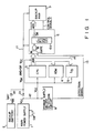
- a main power supply 1 is provided with a switch SW and, when it is turned on, supplies operating power of a potential of approximately Vcc to each component of the system.
- the main power supply 1 is formed by an AC power source, a battery, etc.
- a backup battery 2 acts as a back-up power supply which brings backup power of a potential of about VBK to a memory, etc.
- the output terminals of the main power supply 1 and the back-up battery 2 are connected to power lines 11 via reverse current blocking diodes D1 and D2.
- the output voltage VCC of the main power source 1 is set slightly higher than the output voltage VBK of the back-up battery 2, so that power is fed to the power lines 11 mainly from the main power supply 1 when the switch SW is on, and mainly from the back-up battery 2 when the switch SW is off.
- the output terminal of the main power supply 1 is also connected to power lines 12.
- a CPU (central processing unit) 3, a ROM (read only memory) 4, an I/O port (input/output port) 5 and an address bus 14 are connected to the power lines 12.
- the address bus 14 transfers address data output from the CPU 3 to the ROM 4, I/O port 5, and to a RAM controller 6 to be described later.
- the RAM controller 6 is constantly operative by receiving power fed through the power lines 11.
- the RAM controller 6 receives an address signal from the address bus 14 and makes access to the RAM 7 by supplying the address signals and control signals thereto, or generates an address signal by itself and supplies the address signals and control signals to the RAM 7 to effect refreshment thereof.
- the RAM 7 operates constantly upon feeding of power from the power lines 11 and stores data therein.
- the RAM controller 6 comprises input gates IB formed of NAND gates, control circuit 6A and output gates OB formed of inverters. For ease of understanding, only a single input gate IB is shown in Fig. 1. It should be understood, however, that the input gate IB is arranged in a number corresponding to the number of signals that are fed to the RAM controller 6 and the RAM 7 from the CPU 3, ROM 4, I/O port 5, etc. Also, a plurality of output gates are provided. Input signals are fed to one of the input terminals of each input gate IB and detection signals from a detection circuit to be described hereinafter are fed to the other input terminal of the input gate IB. Address data, control signals, etc. output by the RAM controller 6 are supplied to the RAM 7.
- the CPU 3, ROM 4, I/O port 5 and the address bus 14, already mentioned, are illustrative of circuits to which no back-up power is supplied.
- the above mentioned RAM controller 6 and RAM 7 are an example of circuits which are disposed downstream of the circuits to which no back-up power is supplied, and which operates upon receipt of back-up power and signals from circuits located upstream thereof.
- the detection circuit 8 which detects the on/off state of the main power supply 1 and outputs a detection signal of a binary level, whose level changes rapidly.
- the detection signal is fed via a line 13 to the other of the input terminals of the input buffer IB.
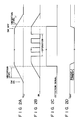
- the output voltage VCC of the main power supply 1 is 0 V as shown in Fig. 2A, so that the CPU 3, ROM 4, I/O port 5, power supply on-off detection circuit 8 and the address bus 14 are inoperative.
- the RAM control circuit 6 and RAM 7 are, as shown in Fig. 2D, supplied a back-up current IBAT from the back-up battery 2 via the power lines 11.
- the back-up current IBAT causes the RAM control circuit 6 and RAM 7 to perform predetermined functions, such as, refreshment.
- the non back-uped circuits such as, the CPU 3 and the address bus 14, are rendered electrically unstable.
- the voltage of the input signal (voltage on the bus 14) of, for example, the RAM controller 6 is, as is apparent from Fig. 2B, put into an indefinite state, i.e., into an unstable state where the voltage is neither at a logic "1" level nor a logic "0" level.
- the detection circuit 8 starts functioning when the output voltage VCC of the main power supply 1 is still at a low level and, as shown in Fig. 2C, continues to output detection signals of a low level (ground level) till the voltage VCC reaches such a level as enables the CPU 3, bus 14, etc. to operate stably.
- the NAND gates forming the input gates IB are closed in response to the detection signal.
- the uncertain level signal from the address bus 14 is inhibited and prevented from being fed to the control circuit 6A.
- the above arrangement prevents penetration current from flowing through the control circuit 6A and RAM 7, so that the back-up current IBAT is maintained approximately at a constant level as shown in Fig. 2D.
- the CPU 3, bus 14, etc. starts normal functions and an input signal to the RAM control circuit 6 is also at a stable voltage level (of a logic 1 or logic 2).
- the detection circuit 8 When the output voltage VCC subsequently reaches the level of a reference voltage, the detection circuit 8 rapidly changes the level of the detection signal into a high level as shown in Fig. 2C, whereby the NAND gates forming the input buffer IB are opened permitting the signal on the bus 14 to be inverted and the signal so inverted to be fed to the control circuit 6, which then controls the RAM 7 on the basis of the signal received.
- the CPU 3 drives the bus 14 and, as shown in Fig. 2B, sends, for example, the address signal to the control circuit 6.
- the level of the address signal is substantially stable so that no penetration current flows into the control circuit 6A, RAM 7, etc.
- the detection circuit 8 When the voltage VCC decreases to a reference value before the CPU 3 and bus 14 start unstable operation, the detection circuit 8 outputs a detection signal of a low level, in response to which the input gates IB are closed and the address signal on the bus 14 ceases to be fed to the control circuit or chip 6A.
- the non backed up circuits 3 and 14 to this embodiment are located upstream of the circuit 6A which is backed up by the back-up power supply 2. Further, owing to the provision of the input buffer IB, the indefinite-level signal resulting from turn-on and turn-off of the main power supply 1 is inhibited from being supplied to the back-uped circuit 6A, thus eliminating the known drawback that the back-up current IBAT is rapidly increased immediately after turn-on and turn-off of the power supply (or that surge current is produced). In other words, a rush current prevention circuit is obtained.
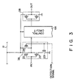
- Fig. 3 illustrates a specific arrangement of the RAM control circuit.
- the input buffer is formed of a first P-type MOS transistor 21, a first N-type MOS transistor 22, a second N-type MOS transistor 23 and a second P-type MOS transistor.
- the first P-type MOS transistor 21 is connected to the power lines 11 at one end of its current path.
- the first N-type MOS transistor 22 has a current path connected at one end to the other end of the current path of the first P-type MOS transistor 21.
- the second N-type MOS transistor 23 is connected at one end of its current path to the other end of the current path of the first N-type MOS transistor 22, and grounded at the other end of its current path.
- the second P-type MOS transistor 24 has a current path coupled at one end to one end of the current path of the first P-type MOS transistor 21 and at the other end to the other end of the current path of the second P-type MOS transistor 24.
- the first P-type MOS transistor 21 and the first N-type MOS transistor 22 constitute an inverter, and are supplied at respective gates with an input signal coming from the address bus 14.
- To the gates of the second N-type MOS transistor 23 and the second P-type MOS transistor 24 are supplied a detection signal.
- the current driving ability of the second P-type MOS transistor 24 and the second N-type MOS transistor 23 is greater than that of the first P-type MOS transistor 21 and the first N-type MOS transistor 22.
- the input buffer OB shown in Fig. 3 is an inverter circuit of a known type.
- the second P-type MOS transistor 24 Upon receipt of a detection signal of a high level, the second P-type MOS transistor 24 turns off and the second N-type MOS transistor 23 turns on, so that the inverter formed of the transistors 21 and 22 turns on and outputs a signal from the address bus 14 in an inverted form.
- the second P-type MOS transistor 24 turns on and the second N-type MOS transistor turns off, so that the output terminal of the input buffer IB is set at a high level, with the result that an input signal of an indefinite level is disabled.
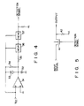
- the power supply voltage VCC and ground voltage are applied to an operational amplifier 31.
- a capacitor 32 is connected between the output terminal of the operational amplifier 31 and ground potential.
- a diode 33 for discharging the charge of the capacitor 32 at the power-off time, and a resistor 34.
- the output terminal of the operational amplifier is connected to inverters (HCl4) 36 and 37 cascade connected to each other in two stages, via a resistor 35 for inhibiting the latch-up of a CMOS circuit.
- a resistor 38 Between the output terminal of the inverter 37 and the ground is connected a resistor 38.
- the above circuit outputs a high level signal when the power voltage VCC exceeds a predetermined value, say, 4.5 V and outputs a low level signal when the voltage VCC becomes 4.5 V or less.
- a predetermined value say, 4.5 V
- Schmitt trigger cells, or the like may be employed for the inverters 36 and 37.
- the input signal according to this embodiment is gated using a detection signal from the detection circuit 8. Accordingly, even if the input signal is at an indefinite level, a signal of an uncertain level is not inputted into the back-uped circuit. In other words, no penetration current flows through the back-uped circuit, thus affording back-up function by a battery over a long period of time and avoiding a back-up voltage drop due to a rapid increase in the back-up current.
- the arrangement of the input buffer IB is not limited to the one shown in Fig. 3.
- the transistors to which the input signal and detection signal are fed may be interchanged.
- the current driving ability of the transistors 21, 22 is set to be greater than that of the transistors 23, 24.
- another circuit arrangement, such as one shown in Fig. 5, is used for the input buffer IB.
- the input signal is supplied to a back-uped circuit through the current path of the MOS transistor 41.
- the MOS transistor 41 is supplied at its gate with the detection signal with its current path coupled at the other end to the back-up circuit and pulled up or pulled down at a predetermined potential Vl via a resistor.
- the input gate IB need not be formed of a NAND gate.
- a two-terminal OR gate may be used as the input buffer IB.
- a high level detection signal is supplied to the OR gate while the input signal remains at an uncertain level.
- an optional circuit which is capable of fixing the input signal at a predetermined level while the level of the input signal stays uncertain may be used as the input buffer IB.
- This invention is not limited to computer devices.
- the invention is for a wide range of circuitry in which both a back-uped circuit 51 and a non back-uped circuit 52 exist as shown in Fig. 6.
- transmission of signals (output signals, control signals, data, addresses) from the non back-uped circuit 52 to the back-uped circuit 51 is inhibited by the inhibiting circuit 53.
- diodes are used as a reverse current blocking circuits of the back-up battery 2.
- the invention is not limited thereto. For example, elements, such as FETs or transistors, may be used instead.
- the detection signal may be generated in the main power supply. Further, it may be generated manually prior to turn-on and turn-off of the main power supply. Still alternatively, a transiendt contact or intermediate contact may be set up in the main power supply, so that the generation of a detection signal is accomplished by using a signal from such transient or intermediate contact.
- the main power supply may be turned on or off after the level of detection signals has been set.
- Detection signals need not be generated by measuring the magnitude of the power supply voltage VCC.
- turn-on and turn-off of the power supply switch may trigger calculating setting a predermined period of time to spend, to inhibit unstable-level signals from flowing through a back-uped circuit for such set period of time during which it is anticipated that the power supply voltage is at an unstable level.
Landscapes
- Engineering & Computer Science (AREA)
- Theoretical Computer Science (AREA)
- Physics & Mathematics (AREA)
- General Engineering & Computer Science (AREA)
- General Physics & Mathematics (AREA)
- Power Sources (AREA)
- Logic Circuits (AREA)
- Electronic Switches (AREA)
- Dram (AREA)
Applications Claiming Priority (2)
| Application Number | Priority Date | Filing Date | Title |
|---|---|---|---|
| JP254964/89 | 1989-09-29 | ||
| JP1254964A JP2862591B2 (ja) | 1989-09-29 | 1989-09-29 | 突入電流防止回路 |
Publications (3)
| Publication Number | Publication Date |
|---|---|
| EP0419902A2 true EP0419902A2 (fr) | 1991-04-03 |
| EP0419902A3 EP0419902A3 (en) | 1994-06-29 |
| EP0419902B1 EP0419902B1 (fr) | 1996-12-27 |
Family
ID=17272316
Family Applications (1)
| Application Number | Title | Priority Date | Filing Date |
|---|---|---|---|
| EP90117109A Expired - Lifetime EP0419902B1 (fr) | 1989-09-29 | 1990-09-05 | Circuit de prévention de courants de pénétration |
Country Status (5)
| Country | Link |
|---|---|
| US (1) | US5140183A (fr) |
| EP (1) | EP0419902B1 (fr) |
| JP (1) | JP2862591B2 (fr) |
| KR (1) | KR930008262B1 (fr) |
| DE (1) | DE69029497T2 (fr) |
Families Citing this family (14)
| Publication number | Priority date | Publication date | Assignee | Title |
|---|---|---|---|---|
| JP3245861B2 (ja) * | 1990-11-19 | 2002-01-15 | セイコーエプソン株式会社 | ドッキングシステム |
| US5313112A (en) * | 1991-12-23 | 1994-05-17 | Ford Motor Company | Low voltage inhibiting circuit for a microcomputer |
| US5369311A (en) * | 1992-03-06 | 1994-11-29 | Intel Corporation | Clock generator control circuit |
| FR2690796B1 (fr) * | 1992-04-30 | 1994-06-17 | Sgs Thomson Microelectronics | Circuit de detection de seuils de tension. |
| JPH06103748A (ja) * | 1992-09-16 | 1994-04-15 | Mitsubishi Electric Corp | Icメモリカードの電源制御回路 |
| US6005436A (en) * | 1992-10-07 | 1999-12-21 | Matsushita Electric Industrial Co., Ltd. | Internal reduced-voltage generator for semiconductor integrated circuit |
| JP2524380Y2 (ja) * | 1992-11-27 | 1997-01-29 | 双葉電子工業株式会社 | ラジコン送信機の電源制御回路 |
| JPH06177678A (ja) * | 1992-12-09 | 1994-06-24 | Toshiba Corp | 電子回路 |
| US5416363A (en) * | 1993-04-22 | 1995-05-16 | Micron Semiconductor, Inc. | Logic circuit initialization |
| US5708388A (en) * | 1994-12-15 | 1998-01-13 | International Business Machines Corporation | Single current source current generating circit for periodically activating and deactivating portions of an IC |
| KR19980054031A (ko) * | 1996-12-27 | 1998-09-25 | 박병재 | 자동차의 도난방지 장치 |
| US7378896B2 (en) * | 2005-05-13 | 2008-05-27 | O2Micro International Ltd. | Single pin for multiple functional control purposes |
| JP2013077962A (ja) * | 2011-09-30 | 2013-04-25 | Renesas Electronics Corp | 論理回路、半導体集積回路 |
| JP6276720B2 (ja) * | 2015-02-06 | 2018-02-07 | 株式会社東芝 | 静電破壊防止回路 |
Family Cites Families (14)
| Publication number | Priority date | Publication date | Assignee | Title |
|---|---|---|---|---|
| US3155847A (en) * | 1963-02-19 | 1964-11-03 | Westinghouse Electric Corp | Circuit for protecting a load circuit from initial power supply voltage transients |
| JPS55115729A (en) * | 1979-02-28 | 1980-09-05 | Toshiba Corp | Mos transistor circuit |
| US4249089A (en) * | 1979-06-27 | 1981-02-03 | Rca Corporation | Short-term power dropout arrangement useful in a television receiver |
| US4288865A (en) * | 1980-02-06 | 1981-09-08 | Mostek Corporation | Low-power battery backup circuit for semiconductor memory |
| US4344003A (en) * | 1980-08-04 | 1982-08-10 | Rca Corporation | Low power voltage multiplier circuit |
| JPS57111120A (en) * | 1980-12-26 | 1982-07-10 | Canon Inc | Reset pulse generator |
| US4617473A (en) * | 1984-01-03 | 1986-10-14 | Intersil, Inc. | CMOS backup power switching circuit |
| US4698530A (en) * | 1984-11-09 | 1987-10-06 | National Semiconductor Corporation | Power switch for dual power supply circuit |
| US4647956A (en) * | 1985-02-12 | 1987-03-03 | Cypress Semiconductor Corp. | Back biased CMOS device with means for eliminating latchup |
| NL8502859A (nl) * | 1985-10-21 | 1987-05-18 | Philips Nv | Schakelingenstelsel met hersynchronisatie van gegevens. |
| JPH0650815B2 (ja) * | 1986-04-25 | 1994-06-29 | 日本電気株式会社 | 論理回路 |
| JPS6336350A (ja) * | 1986-07-30 | 1988-02-17 | Toshiba Mach Co Ltd | Cmosインタフエ−スのラツチアツプ防止回路 |
| US4831595A (en) * | 1987-05-06 | 1989-05-16 | Hughes Aircraft Company | Low voltage power down logic control circuit |
| US4902910A (en) * | 1987-11-17 | 1990-02-20 | Xilinx, Inc. | Power supply voltage level sensing circuit |
-
1989
- 1989-09-29 JP JP1254964A patent/JP2862591B2/ja not_active Expired - Fee Related
-
1990
- 1990-09-05 EP EP90117109A patent/EP0419902B1/fr not_active Expired - Lifetime
- 1990-09-05 DE DE69029497T patent/DE69029497T2/de not_active Expired - Fee Related
- 1990-09-06 US US07/578,223 patent/US5140183A/en not_active Expired - Lifetime
- 1990-09-07 KR KR1019900014231A patent/KR930008262B1/ko not_active Expired - Fee Related
Also Published As
| Publication number | Publication date |
|---|---|
| JPH03116313A (ja) | 1991-05-17 |
| KR930008262B1 (ko) | 1993-08-27 |
| DE69029497D1 (de) | 1997-02-06 |
| EP0419902A3 (en) | 1994-06-29 |
| US5140183A (en) | 1992-08-18 |
| JP2862591B2 (ja) | 1999-03-03 |
| EP0419902B1 (fr) | 1996-12-27 |
| DE69029497T2 (de) | 1997-07-10 |
| KR910006826A (ko) | 1991-04-30 |
Similar Documents
| Publication | Publication Date | Title |
|---|---|---|
| US6448812B1 (en) | Pull up/pull down logic for holding a defined value during power down mode | |
| EP0440204B1 (fr) | Dispositif de circuit intégré à semi-conducteurs avec un terminal d'alimentation principal et un terminal d'alimentation de sauvegarde indépendants l'un de l'autre | |
| US6058063A (en) | Integrated circuit memory devices having reduced power consumption requirements during standby mode operation | |
| EP0137933B1 (fr) | Circuit de commande à trois états destiné à la précharge de lignes de signal | |
| US20020000872A1 (en) | Method and apparatus for reducing standby leakage current using a leakage control transistor that receives boosted gate drive during an active mode | |
| EP0419902A2 (fr) | Circuit de prévention de courants de pénétration | |
| KR910006471B1 (ko) | 리세트 신호 발생회로 | |
| US4275312A (en) | MOS decoder logic circuit having reduced power consumption | |
| US4948995A (en) | Disenabling circuit for power-on event | |
| US5650741A (en) | Power line connection circuit and power line switch IC for the same | |
| US5552719A (en) | Output buffer circuit having gate voltage control circuit of gate current controlling transistor connected to output transistor | |
| US5801569A (en) | Output driver for mixed supply voltage systems | |
| US6335648B1 (en) | Circuit using internal pull-up/pull-down resistor during reset | |
| EP1034619B1 (fr) | Circuit de reenclenchement d'alimentation a puissance nulle | |
| US4529895A (en) | Active high before open three state integrated circuit output stage | |
| US4347448A (en) | Buffer circuit for semiconductor memory | |
| US5101119A (en) | CMOS type input buffer circuit for semiconductor device and semiconductor device with the same | |
| US6005424A (en) | Integrated power switch for parasitically powered devices | |
| US5210449A (en) | Edge triggered tri-state output buffer | |
| US5610544A (en) | Semiconductor integrated circuit free from through current due to source-voltage drop | |
| US4894558A (en) | Power saving input buffer for use with a gate array | |
| JP3311751B2 (ja) | 低電力型電圧感知回路 | |
| JPH09252245A (ja) | 回路ドライバおよび保護回路 | |
| US4488266A (en) | Low-power address decoder | |
| US5111073A (en) | Wafer-scale semiconductor device having fail-safe circuit |
Legal Events
| Date | Code | Title | Description |
|---|---|---|---|
| PUAI | Public reference made under article 153(3) epc to a published international application that has entered the european phase |
Free format text: ORIGINAL CODE: 0009012 |
|
| 17P | Request for examination filed |
Effective date: 19901002 |
|
| AK | Designated contracting states |
Kind code of ref document: A2 Designated state(s): DE FR GB |
|
| PUAL | Search report despatched |
Free format text: ORIGINAL CODE: 0009013 |
|
| AK | Designated contracting states |
Kind code of ref document: A3 Designated state(s): DE FR GB |
|
| 17Q | First examination report despatched |
Effective date: 19950308 |
|
| GRAG | Despatch of communication of intention to grant |
Free format text: ORIGINAL CODE: EPIDOS AGRA |
|
| GRAH | Despatch of communication of intention to grant a patent |
Free format text: ORIGINAL CODE: EPIDOS IGRA |
|
| GRAH | Despatch of communication of intention to grant a patent |
Free format text: ORIGINAL CODE: EPIDOS IGRA |
|
| GRAA | (expected) grant |
Free format text: ORIGINAL CODE: 0009210 |
|
| AK | Designated contracting states |
Kind code of ref document: B1 Designated state(s): DE FR GB |
|
| REF | Corresponds to: |
Ref document number: 69029497 Country of ref document: DE Date of ref document: 19970206 |
|
| ET | Fr: translation filed | ||
| PLBE | No opposition filed within time limit |
Free format text: ORIGINAL CODE: 0009261 |
|
| STAA | Information on the status of an ep patent application or granted ep patent |
Free format text: STATUS: NO OPPOSITION FILED WITHIN TIME LIMIT |
|
| 26N | No opposition filed | ||
| REG | Reference to a national code |
Ref country code: GB Ref legal event code: IF02 |
|
| PGFP | Annual fee paid to national office [announced via postgrant information from national office to epo] |
Ref country code: FR Payment date: 20080915 Year of fee payment: 19 |
|
| PGFP | Annual fee paid to national office [announced via postgrant information from national office to epo] |
Ref country code: GB Payment date: 20080910 Year of fee payment: 19 |
|
| PGFP | Annual fee paid to national office [announced via postgrant information from national office to epo] |
Ref country code: DE Payment date: 20080919 Year of fee payment: 19 |
|
| GBPC | Gb: european patent ceased through non-payment of renewal fee |
Effective date: 20090905 |
|
| REG | Reference to a national code |
Ref country code: FR Ref legal event code: ST Effective date: 20100531 |
|
| PG25 | Lapsed in a contracting state [announced via postgrant information from national office to epo] |
Ref country code: DE Free format text: LAPSE BECAUSE OF NON-PAYMENT OF DUE FEES Effective date: 20100401 Ref country code: FR Free format text: LAPSE BECAUSE OF NON-PAYMENT OF DUE FEES Effective date: 20090930 |
|
| PG25 | Lapsed in a contracting state [announced via postgrant information from national office to epo] |
Ref country code: GB Free format text: LAPSE BECAUSE OF NON-PAYMENT OF DUE FEES Effective date: 20090905 |