EP0417573A2 - Abstandshalter- und Dichtungsanordnung für Flüssigkristall-Lichtventil - Google Patents
Abstandshalter- und Dichtungsanordnung für Flüssigkristall-Lichtventil Download PDFInfo
- Publication number
- EP0417573A2 EP0417573A2 EP90116782A EP90116782A EP0417573A2 EP 0417573 A2 EP0417573 A2 EP 0417573A2 EP 90116782 A EP90116782 A EP 90116782A EP 90116782 A EP90116782 A EP 90116782A EP 0417573 A2 EP0417573 A2 EP 0417573A2
- Authority
- EP
- European Patent Office
- Prior art keywords
- liquid crystal
- layer
- light valve
- cement
- particles
- Prior art date
- Legal status (The legal status is an assumption and is not a legal conclusion. Google has not performed a legal analysis and makes no representation as to the accuracy of the status listed.)
- Withdrawn
Links
- 239000004973 liquid crystal related substance Substances 0.000 title claims abstract description 124
- 238000007789 sealing Methods 0.000 title claims abstract description 30
- 239000004568 cement Substances 0.000 claims abstract description 40
- 230000003287 optical effect Effects 0.000 claims abstract description 20
- 229920000642 polymer Polymers 0.000 claims abstract description 14
- 125000006850 spacer group Chemical group 0.000 claims description 43
- 238000000034 method Methods 0.000 claims description 27
- 239000000463 material Substances 0.000 claims description 20
- 239000000853 adhesive Substances 0.000 claims description 18
- 230000001070 adhesive effect Effects 0.000 claims description 18
- 239000002245 particle Substances 0.000 claims description 18
- 230000002093 peripheral effect Effects 0.000 claims description 16
- 238000004519 manufacturing process Methods 0.000 claims description 12
- 239000000203 mixture Substances 0.000 claims description 8
- GZVHEAJQGPRDLQ-UHFFFAOYSA-N 6-phenyl-1,3,5-triazine-2,4-diamine Chemical compound NC1=NC(N)=NC(C=2C=CC=CC=2)=N1 GZVHEAJQGPRDLQ-UHFFFAOYSA-N 0.000 claims description 6
- 230000005855 radiation Effects 0.000 claims description 3
- 238000003825 pressing Methods 0.000 claims 2
- 239000002861 polymer material Substances 0.000 claims 1
- QVGXLLKOCUKJST-UHFFFAOYSA-N atomic oxygen Chemical compound [O] QVGXLLKOCUKJST-UHFFFAOYSA-N 0.000 abstract description 6
- 229910052760 oxygen Inorganic materials 0.000 abstract description 6
- 239000001301 oxygen Substances 0.000 abstract description 6
- 238000009792 diffusion process Methods 0.000 abstract description 5
- 230000001681 protective effect Effects 0.000 abstract description 2
- 238000012360 testing method Methods 0.000 description 7
- VYPSYNLAJGMNEJ-UHFFFAOYSA-N Silicium dioxide Chemical compound O=[Si]=O VYPSYNLAJGMNEJ-UHFFFAOYSA-N 0.000 description 5
- 230000000903 blocking effect Effects 0.000 description 4
- 230000015556 catabolic process Effects 0.000 description 4
- 239000000306 component Substances 0.000 description 4
- 238000006731 degradation reaction Methods 0.000 description 4
- 239000004005 microsphere Substances 0.000 description 4
- 238000003860 storage Methods 0.000 description 4
- 239000000758 substrate Substances 0.000 description 4
- VVQNEPGJFQJSBK-UHFFFAOYSA-N Methyl methacrylate Chemical compound COC(=O)C(C)=C VVQNEPGJFQJSBK-UHFFFAOYSA-N 0.000 description 3
- 229920005372 Plexiglas® Polymers 0.000 description 3
- 238000010586 diagram Methods 0.000 description 3
- 230000004048 modification Effects 0.000 description 3
- 238000012986 modification Methods 0.000 description 3
- 239000000377 silicon dioxide Substances 0.000 description 3
- XUIMIQQOPSSXEZ-UHFFFAOYSA-N Silicon Chemical compound [Si] XUIMIQQOPSSXEZ-UHFFFAOYSA-N 0.000 description 2
- 229910052681 coesite Inorganic materials 0.000 description 2
- 229910052906 cristobalite Inorganic materials 0.000 description 2
- 238000005516 engineering process Methods 0.000 description 2
- 239000000835 fiber Substances 0.000 description 2
- 239000010408 film Substances 0.000 description 2
- 239000011521 glass Substances 0.000 description 2
- 238000010438 heat treatment Methods 0.000 description 2
- AMGQUBHHOARCQH-UHFFFAOYSA-N indium;oxotin Chemical compound [In].[Sn]=O AMGQUBHHOARCQH-UHFFFAOYSA-N 0.000 description 2
- 239000007788 liquid Substances 0.000 description 2
- 238000007433 macroscopic evaluation Methods 0.000 description 2
- 239000011159 matrix material Substances 0.000 description 2
- 229910052751 metal Inorganic materials 0.000 description 2
- 239000002184 metal Substances 0.000 description 2
- 239000005304 optical glass Substances 0.000 description 2
- 230000004044 response Effects 0.000 description 2
- 229910052710 silicon Inorganic materials 0.000 description 2
- 239000010703 silicon Substances 0.000 description 2
- 235000012239 silicon dioxide Nutrition 0.000 description 2
- 229910052682 stishovite Inorganic materials 0.000 description 2
- 229910052905 tridymite Inorganic materials 0.000 description 2
- 230000000007 visual effect Effects 0.000 description 2
- 229910052724 xenon Inorganic materials 0.000 description 2
- FHNFHKCVQCLJFQ-UHFFFAOYSA-N xenon atom Chemical compound [Xe] FHNFHKCVQCLJFQ-UHFFFAOYSA-N 0.000 description 2
- 235000009917 Crataegus X brevipes Nutrition 0.000 description 1
- 235000013204 Crataegus X haemacarpa Nutrition 0.000 description 1
- 235000009685 Crataegus X maligna Nutrition 0.000 description 1
- 235000009444 Crataegus X rubrocarnea Nutrition 0.000 description 1
- 235000009486 Crataegus bullatus Nutrition 0.000 description 1
- 235000017181 Crataegus chrysocarpa Nutrition 0.000 description 1
- 235000009682 Crataegus limnophila Nutrition 0.000 description 1
- 235000004423 Crataegus monogyna Nutrition 0.000 description 1
- 240000000171 Crataegus monogyna Species 0.000 description 1
- 235000002313 Crataegus paludosa Nutrition 0.000 description 1
- 235000009840 Crataegus x incaedua Nutrition 0.000 description 1
- 206010052804 Drug tolerance Diseases 0.000 description 1
- 230000009471 action Effects 0.000 description 1
- 230000004913 activation Effects 0.000 description 1
- 239000002313 adhesive film Substances 0.000 description 1
- 229910052782 aluminium Inorganic materials 0.000 description 1
- XAGFODPZIPBFFR-UHFFFAOYSA-N aluminium Chemical compound [Al] XAGFODPZIPBFFR-UHFFFAOYSA-N 0.000 description 1
- 230000008859 change Effects 0.000 description 1
- 229910052729 chemical element Inorganic materials 0.000 description 1
- 239000011248 coating agent Substances 0.000 description 1
- 238000000576 coating method Methods 0.000 description 1
- 230000008878 coupling Effects 0.000 description 1
- 238000010168 coupling process Methods 0.000 description 1
- 238000005859 coupling reaction Methods 0.000 description 1
- 230000007547 defect Effects 0.000 description 1
- 230000006866 deterioration Effects 0.000 description 1
- 238000009826 distribution Methods 0.000 description 1
- 230000000694 effects Effects 0.000 description 1
- 238000011156 evaluation Methods 0.000 description 1
- 230000008020 evaporation Effects 0.000 description 1
- 238000001704 evaporation Methods 0.000 description 1
- 230000004927 fusion Effects 0.000 description 1
- 239000000499 gel Substances 0.000 description 1
- 238000003384 imaging method Methods 0.000 description 1
- 239000011261 inert gas Substances 0.000 description 1
- 239000000155 melt Substances 0.000 description 1
- 238000002156 mixing Methods 0.000 description 1
- 238000006303 photolysis reaction Methods 0.000 description 1
- 238000012545 processing Methods 0.000 description 1
- 239000011347 resin Substances 0.000 description 1
- 229920005989 resin Polymers 0.000 description 1
- 230000000717 retained effect Effects 0.000 description 1
- 238000012216 screening Methods 0.000 description 1
- 239000000565 sealant Substances 0.000 description 1
- 229910052814 silicon oxide Inorganic materials 0.000 description 1
- 239000007787 solid Substances 0.000 description 1
- 239000010409 thin film Substances 0.000 description 1
Images

Classifications
-
- G—PHYSICS
- G02—OPTICS
- G02F—OPTICAL DEVICES OR ARRANGEMENTS FOR THE CONTROL OF LIGHT BY MODIFICATION OF THE OPTICAL PROPERTIES OF THE MEDIA OF THE ELEMENTS INVOLVED THEREIN; NON-LINEAR OPTICS; FREQUENCY-CHANGING OF LIGHT; OPTICAL LOGIC ELEMENTS; OPTICAL ANALOGUE/DIGITAL CONVERTERS
- G02F1/00—Devices or arrangements for the control of the intensity, colour, phase, polarisation or direction of light arriving from an independent light source, e.g. switching, gating or modulating; Non-linear optics
- G02F1/01—Devices or arrangements for the control of the intensity, colour, phase, polarisation or direction of light arriving from an independent light source, e.g. switching, gating or modulating; Non-linear optics for the control of the intensity, phase, polarisation or colour
- G02F1/13—Devices or arrangements for the control of the intensity, colour, phase, polarisation or direction of light arriving from an independent light source, e.g. switching, gating or modulating; Non-linear optics for the control of the intensity, phase, polarisation or colour based on liquid crystals, e.g. single liquid crystal display cells
- G02F1/133—Constructional arrangements; Operation of liquid crystal cells; Circuit arrangements
- G02F1/1333—Constructional arrangements; Manufacturing methods
- G02F1/1339—Gaskets; Spacers; Sealing of cells
Definitions
- the present invention generally relates to the field of electro-optical liquid crystal devices, and more specifically to a method of spacing and sealing in the manufacture of liquid crystal light valves.
- the liquid crystal light valve is an optical-to-optical image transducer that is capable of accepting a low-intensity visible light image and converting it, in real time, into an output image with light from another source.
- LCLV liquid crystal light valve
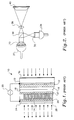
- a generic LCLV is generally designated by the reference numeral 10, as viewed in Figure 1, which is a fragmentary section through an edge portion of the device.
- the LCLV 10 comprises a CdS or silicon photoconductor layer 12 and a nematic (normally transparent) liquid crystal layer 14 separated by a light blocking layer 16 and a dielectric mirror layer 18.
- the photoconductor layer 12 acts as an imaging, light-controlled voltage modulator for the liquid crystal layer 14.
- the liquid crystal layer 14 is 2-10 micrometers thick.
- the broad-spectral-band dielectric mirror 18 serves to reflect the modulated readout light, and the light-blocking layer 16 prevents residual read-out light from reaching the photoconductor layer 12.
- the impedance of the photoconductor layer 12 lowers and the voltage applied by a bias voltage source 20 between a transparent conductive electrode layer 22 and a transparent conductive counter electrode layer 24 is switched to the liquid crystal layer 14.
- This drives the liquid crystal layer 14 above its electro-optic threshold in a pattern that replicates the input image intensity, including grey-scale levels.
- Typical operating voltage levels are 10 V rms at 10 kHz.
- the light valve 10 further comprises liquid crystal alignment film layers 26 and 27 formed on the opposite surfaces of the liquid crystal layer 14, and transparent protective substrate face plates 28 and 30.
- Face plates 28 and 30 are made of optical glass flats or fiberoptics, and sandwich the liquid crystal and associated assembly layers therebetween to provide coupling between input and output light.
- the transparent electrode layers 22 and 24 are typically made of indium tin oxide (ITO).
- FIG. 2 A typical optical system for use of the liquid crystal light valve 10 in a large-screen display application is illustrated in Figure 2.
- An optical system 32 collimates light from a xenon arc lamp 34 and directs it to a beam splitter 36, where it is polarized.
- the beam splitter 36 directs the light beam to the light valve 10 where it is phase-modulated with the image information from a cathode ray tube display 37 by the liquid crystal layer 14.
- the light is then reflected by the light valve dielectric mirror 18 back to the beam splitter 36, which now acts as an analyzer to create an intensity image.
- a projection lens 38 focusses the image on a distant screen 40.
- Liquid crystal light valves are widely utilized in applications which involve severe high and low temperature storage conditions. It is therefore desirable to maximize the operating lifetime and stability of the devices. It is required to very accurately control the spacing or thickness of the liquid crystal layer during fabrication to provide the necessary operating tolerances. Both of these functions have been difficult and expensive to achieve with existing technology.
- Liquid crystal layers used in LCLV's have often not been sealed.
- the face plates 28 and 30 are optical flats with extremely precise surfaces, which cause the liquid crystal material therebetween to be retained by capillary action.
- unsealed LCLV's suffer from limited lifetime due to diffusion of oxygen and moisture into the liquid crystal material.
- the volatile components of the liquid crystal material become progressively depleted due to evaporation. All of these effects result in degradation of the photostability of the LCLV and are accelerated by the high temperature conditions under which the LCLV's may operate.
- the xenon arc lamp 34 which is used in the projection system, for example, operates at a power level of 400 to 1600. watts, causing heating of the LCLV.
- such layers have remained unsealed due to the difficulty in obtaining thickness control of the LC layer 14.
- the liquid crystal layer In addition to preventing degradation of the liquid crystal material in LCLV's, the liquid crystal layer must be of precise thickness.
- One method of providing thickness control is by forming a number of small, hard spacer pads 42 made of silicon or SiO x distributed in an even pattern on the periphery of the face plate 28 as illustrated in Figure 4.
- the disadvantage of this arrangement is that spacer pads 42 having a thickness in excess of approximately 6 micrometers are very time consuming and expensive to form. Further, the spacer pads 42 are too small and spaced at too large intervals to provide any sealing function.
- U.S. Patent no. 4,114,991 to Bleha et al shows a general arrangement of this type.
- fiber spacer rods and polymer spheres have become commercially available with accurately known diameters. They range between 2 and 25 micrometers in thickness (diameter) and are therefore well suited for the spacing of ordinary liquid crystal displays, as previously practiced in the art, merely by dispersing the spacers in the liquid crystal material. In high resolution displays using liquid crystal light valves, however, the spacers can not be doped into the bulk liquid crystal material since they would be visible on the screen. This particular expedient is found in U.S. Patent no. 4,470,668 to Inoue et al.
- a purpose of the present invention is to provide a simple and low cost spacing and sealing method for liquid crystal light valve fabrication which substantially increases the operating lifetime and stability of the device under extreme high and low temperature conditions, and retains all of the components of the liquid crystal assembly within the device at a wide range of vapor pressures.
- Another purpose of the present invention is to provide a spacing and sealing method for liquid crystal light valve fabrication which automatically establishes accurate spacing of the liquid crystal layer in the device, effectively seals the device against diffusion of oxygen and moisture into the device during and after fabrication, enables precise thickness control merely through selection of polymer spheres of the desired thickness, and utilizes polymer spheres having an accurately predetermined diameter in a novel manner.
- the invention also includes a liquid crystal light valve fabricated in accordance with the present method.
- polymer spheres are dispersed in an optical adhesive or cement.
- the spheres have an accurately known diameter corresponding to the desired thickness of a liquid crystal layer in a liquid crystal light valve.
- the cement with the polymer spheres dispersed therein is applied around the peripheries of facing surface members which retain the liquid crystal layer, thereby automatically providing the desired thickness or spacing for the liquid crystal layer and sealing the device against oxygen and moisture diffusion into the liquid crystal light valve.
- a liquid crystal light valve fabricated in accordance with the present invention is illustrated in Figure 5 and designated by the reference numeral 50, with component elements designated by the same reference numerals used in Figures l to 4.
- the LCLV 50 is generally disk shaped as shown in Figure 2, with only an edge portion of the LCLV 50 being illustrated in section in Figure 5.
- the novel feature of the present invention involves replacing the spacer pads 42 of the prior art with a sealing spacer 52 which comprises a plurality of polymer spheres 54 of uniform diameter imbedded in an optical cement or adhesive 56, the cement being hardened onto the peripheral surface of the alignment layer 26 which is formed on the face plate 28.
- the spheres 54 are substantially flush with the facing surfaces of the alignment layers 26 and 27, thereby providing automatic and highly accurate spacing of the liquid crystal layer 14.
- the cement 56 in combination with the spheres 54 effectively seals the edges of the liquid crystal layer 14 against inward diffusion of oxygen and moisture during and after fabrication.
- the thickness of the liquid crystal layer 14 may be precisely controlled by the selection of polymer spheres 54 having the desired thickness.
- the method of fabricating a liquid crystal light valve in accordance with the present invention comprises the following steps.
- a method of filling the LCLV with liquid crystal material to accomplish step (g), is to form the sealing spacer 52 in the method described below in which one gap exists, between the space defined within the sealing spacer 52 and the atmosphere.
- the LCLV assembly and liquid crystal are placed in a vacuum chamber, evacuated, and then the unfilled sealed LV at the gap contacted with the liquid crystal material. Fill the vacuum chamber to atmospheric pressure, thereby forcing the liquid crystal material into the evacuated space through the opening to fill the space. Finally, the opening or gap is sealed by, for example, a polymer or metal plug.
- the opening may be formed through one of the face plates 28 and 30, rather than through the sealing spacer 52.
- any liquid, gel, or solid adhesive or cement which is capable of being thermally or ultraviolet cured is embraced by the scope of the invention
- an optical cement which is inert to liquid crystal material and is ultraviolet curable is preferred.
- An example of a commercially available cement is Norland NOA61 optical cement.
- a preferred material for the spheres is Epostar GP-100 balls made of benzoguanamine which are available from EM Industries of Hawthorn, New York. The spheres are dispersed by mechanical mixing in the cement at a volume ratio of 0.1% to 3%.
- step (c) above includes applying the cement 56 in liquid form with the spheres 54 dispersed therein onto the peripheral area of the electrode layer 24 (or onto the overlying alignment layer 26 if provided) on the face plate 28.
- a release plate or block (not shown) coated with a material to which the cement 56 does not adhere is pressed onto the face plate 28 so that the cement 56 is compressed down to the thickness of the spheres 54.
- the cement 56 is then cured or hardened through exposure to ultraviolet radiation, and the release member removed to leave the finished spacer 52.
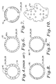
- the sealing spacer 52 may be provided in a number of different configurations, as shown in Figures 6 to 9.
- Figure 6 illustrates a spacer 60 formed on the periphery of the electrode 24 in the form of a plurality of small circular microdrops or dots 60a. There are many spheres 54 dispersed inside each dot 60a, as illustrated in Figure 10.
- Figure 7 illustrates another spacer 70 comprising three equally spaced, relatively large arcuate sections 70a. Although the number of arcuate sections 70a is shown as being three, two or more than three sections may be provided.
- Figure 8 illustrates another sealing spacer 80 in the form of a continuous circular arc, providing complete sealing, to be used with an opening through one of the face plates.
- Figure 9 illustrates a modification of the spacer of Figure 8, designated by the reference numeral 80′, which is formed with a small gap 80a for removal of air and introduction of the liquid crystal by the back-filling method.
- a 1 weight % of Epostar GP-50 (5 micrometers diameter) benzoguanamine resin based microspheres were dispersed in Norland NOA68 optical cement.
- a narrow ribbon of this mixture was placed on the perimeter of an ITO/SiO2 alignment layer coated optical flat 0.5 inch thick and 2.5 inches in diameter), leaving a small gap for a filling hole, as shown in Figure 9.
- a second optical flat of the same type was placed on top and clamped together to limit the spacing to the microsphere size.
- the optical cement was cured with ultraviolet light for 10 minutes. This pre-sealed test cell was placed in a vacuum chamber above a liquid crystal container, and the system was evacuated.
- the glass test cell was lowered to contact the filling hole with the liquid crystal material, and the system was slowly back-filled with inert gas to atmospheric pressure, forcing the LC into the test cell's cavity.
- the filling gap was sealed with optical cement. Evaluation of this sealed LC cell showed uniform spacing and good liquid crystal alignment by macroscopic evaluation (no alignment degradation due to the sealing procedure).
- test cell was presealed with microspheres dispersed in Norland NOA68 optical cement, the same as in Example 1, but the liquid crystal was back-filled at 56°C temperature.
- the elevated temperature reduced the LC viscosity, improved its flow properties, and gave good liquid crystal surface alignment.
- the test cell's spacing was measured at three points prior to and after filling the cell with LC, resulting in average spacing of 4.5 ⁇ 0.1 and 4.3 ⁇ 0.5 respectively.
- the perimeter spacer/seal was pinhole free, since it passed a 144 hour vacuum test without leakage or deterioration. Surface alignment of the liquid crystal was very good, by macroscopic evaluation.
- a liquid crystal light valve was presealed with controlled microsphere spacing, evacuated, back-filled with liquid crystal, and final sealed.
- This sealed LCLV showed excellent pinhole free sealing, good visual alignment quality and uniform electrical activation.
- the LV was fabricated from a photoconductor substrate (ITO/CdS photoconductor/light blocking layer/dielectric mirror/SiO2/alignment layer coated optical flat) with an ITO/SiO2/alignment layer coated counter electrode on optical flat (glass substrates same as in Example 1). The two substrates were clamped together, their spacing controlled by the 5 micron diameter polymer spheres dispersed in Norland NOA68 sealant placed around the perimeter of the counter electrode, leaving a small gap for filling.
- An important application of the present invention is the fabrication of sealed liquid crystal light valves to improve the LCLV lifetime for storage and operation at elevated temperature.
- the hermetically sealed cells will contain all liquid crystal components within the liquid crystal, regardless of their vapor pressure, and retain constant controlled liquid crystal composition at low or high temperatures, during storage or actual operation.
- the improved photostability of the liquid crystal material in sealed experimental test cells has been demonstrated and shown to result in lifetimes on the order of 3 to 4 times that of demountable control cells, using the same alignment technique and liquid crystal material.
- the present invention may be practiced otherwise than as specifically described.
- the polymer spheres may be replaced by other particles such as fibers or rods, although the spheres are preferred because there is less chance of crossover, there is no multiple stacking due to the round geometry, and no sharp edges are produced which would be visible as defects.
- the invention may be applied to a metal matrix type LCLV in which the dielectric mirror is replaced by a matrix of aluminum pads which cover approximately 80% of the back surface of the photoconductive layer.
- the light blocking layer is omitted since ultraviolet readout light is used which does not affect the photoconductive layer.
Landscapes
- Physics & Mathematics (AREA)
- Nonlinear Science (AREA)
- Mathematical Physics (AREA)
- Chemical & Material Sciences (AREA)
- Crystallography & Structural Chemistry (AREA)
- General Physics & Mathematics (AREA)
- Optics & Photonics (AREA)
- Liquid Crystal (AREA)
Applications Claiming Priority (2)
| Application Number | Priority Date | Filing Date | Title |
|---|---|---|---|
| US40570689A | 1989-09-11 | 1989-09-11 | |
| US405706 | 1989-09-11 |
Publications (2)
| Publication Number | Publication Date |
|---|---|
| EP0417573A2 true EP0417573A2 (de) | 1991-03-20 |
| EP0417573A3 EP0417573A3 (en) | 1991-12-27 |
Family
ID=23604867
Family Applications (1)
| Application Number | Title | Priority Date | Filing Date |
|---|---|---|---|
| EP19900116782 Withdrawn EP0417573A3 (en) | 1989-09-11 | 1990-08-31 | Spacing and sealing arrangement for liquid crystal light valve |
Country Status (3)
| Country | Link |
|---|---|
| EP (1) | EP0417573A3 (de) |
| JP (1) | JPH03105323A (de) |
| KR (1) | KR910006764A (de) |
Cited By (2)
| Publication number | Priority date | Publication date | Assignee | Title |
|---|---|---|---|---|
| US6049370A (en) * | 1993-01-26 | 2000-04-11 | Hughes Aircraft Company | Liquid crystal light valves using internal, fixed spacers and method of incorporating same |
| CN111897165A (zh) * | 2019-05-06 | 2020-11-06 | 康惠(惠州)半导体有限公司 | 超微线间距的红外液晶光阀及其制造方法 |
Families Citing this family (1)
| Publication number | Priority date | Publication date | Assignee | Title |
|---|---|---|---|---|
| US6951715B2 (en) * | 2000-10-30 | 2005-10-04 | Sru Biosystems, Inc. | Optical detection of label-free biomolecular interactions using microreplicated plastic sensor elements |
Family Cites Families (4)
| Publication number | Priority date | Publication date | Assignee | Title |
|---|---|---|---|---|
| JPS5827126A (ja) * | 1981-08-11 | 1983-02-17 | Nec Corp | 液晶表示パネルの製造方法 |
| JPS59131A (ja) * | 1982-06-25 | 1984-01-05 | Toshiba Corp | 液晶表示装置の組立装置 |
| JPS60200228A (ja) * | 1984-03-24 | 1985-10-09 | Nippon Shokubai Kagaku Kogyo Co Ltd | 液晶表示装置用スペ−サ− |
| US4925276A (en) * | 1987-05-01 | 1990-05-15 | Electrohome Limited | Liquid crystal light valve utilizing hydrogenated amorphous silicon photodiode |
-
1990
- 1990-08-31 EP EP19900116782 patent/EP0417573A3/en not_active Withdrawn
- 1990-09-10 KR KR1019900014265A patent/KR910006764A/ko not_active Ceased
- 1990-09-11 JP JP2241038A patent/JPH03105323A/ja active Pending
Cited By (2)
| Publication number | Priority date | Publication date | Assignee | Title |
|---|---|---|---|---|
| US6049370A (en) * | 1993-01-26 | 2000-04-11 | Hughes Aircraft Company | Liquid crystal light valves using internal, fixed spacers and method of incorporating same |
| CN111897165A (zh) * | 2019-05-06 | 2020-11-06 | 康惠(惠州)半导体有限公司 | 超微线间距的红外液晶光阀及其制造方法 |
Also Published As
| Publication number | Publication date |
|---|---|
| JPH03105323A (ja) | 1991-05-02 |
| EP0417573A3 (en) | 1991-12-27 |
| KR910006764A (ko) | 1991-04-30 |
Similar Documents
| Publication | Publication Date | Title |
|---|---|---|
| EP0641457B1 (de) | Flüssigkristallzelle mit distanzelementen und verfahren zu ihrer herstellung | |
| US7199855B2 (en) | Liquid crystal display and method of fabricating the same | |
| US5680186A (en) | Liquid crystal display device with microlenses having a focal point between a cover layer and the liquid crystal layer's center | |
| KR20010094969A (ko) | 액정표시장치 및 그 제조방법 | |
| US7145628B2 (en) | Method for fabricating a liquid crystal panel comprising spacers having an initial size larger than an appropriate cell gap | |
| EP0417573A2 (de) | Abstandshalter- und Dichtungsanordnung für Flüssigkristall-Lichtventil | |
| JPH09258176A (ja) | 曲面パネルおよびその製造方法 | |
| JPH10301115A (ja) | 液晶表示素子及びその製造方法 | |
| JP2522549B2 (ja) | 貼り合わせ構造 | |
| JP2832123B2 (ja) | 液晶表示装置 | |
| JP3939571B2 (ja) | 光通信用液晶スイッチと光変調素子 | |
| JP2786564B2 (ja) | 空間光変調素子の製造方法 | |
| JPH09329783A (ja) | 空間光変調素子 | |
| JPS61500136A (ja) | ライトバルブ | |
| JPH0943625A (ja) | 液晶表示デバイス及びその製造方法 | |
| JPH0854634A (ja) | 液晶光学素子及びその製造方法 | |
| JPH06235910A (ja) | 強誘電性液晶表示パネルおよびその製造方法 | |
| JPH08160437A (ja) | 液晶表示装置およびその製造方法 | |
| JPS61160721A (ja) | 液晶表示装置 | |
| JPH049009A (ja) | 空間光変調素子 | |
| JPS61160722A (ja) | 液晶表示装置作製方法 | |
| JPH04172321A (ja) | 液晶電気光学素子 | |
| JPS61160719A (ja) | 液晶表示パネル作製方法 | |
| JPH05333365A (ja) | 空間光変調素子とその製造方法 | |
| JPH09127488A (ja) | 高分子分散型液晶表示パネルとその製造方法 |
Legal Events
| Date | Code | Title | Description |
|---|---|---|---|
| PUAI | Public reference made under article 153(3) epc to a published international application that has entered the european phase |
Free format text: ORIGINAL CODE: 0009012 |
|
| AK | Designated contracting states |
Kind code of ref document: A2 Designated state(s): DE FR GB NL |
|
| PUAL | Search report despatched |
Free format text: ORIGINAL CODE: 0009013 |
|
| AK | Designated contracting states |
Kind code of ref document: A3 Designated state(s): DE FR GB NL |
|
| STAA | Information on the status of an ep patent application or granted ep patent |
Free format text: STATUS: THE APPLICATION IS DEEMED TO BE WITHDRAWN |
|
| 18D | Application deemed to be withdrawn |
Effective date: 19920628 |