EP0406900A2 - Treiberschaltung für eine Flüssigkristallanzeige - Google Patents
Treiberschaltung für eine Flüssigkristallanzeige Download PDFInfo
- Publication number
- EP0406900A2 EP0406900A2 EP90112963A EP90112963A EP0406900A2 EP 0406900 A2 EP0406900 A2 EP 0406900A2 EP 90112963 A EP90112963 A EP 90112963A EP 90112963 A EP90112963 A EP 90112963A EP 0406900 A2 EP0406900 A2 EP 0406900A2
- Authority
- EP
- European Patent Office
- Prior art keywords
- liquid crystal
- signal
- driver
- pulse
- line
- Prior art date
- Legal status (The legal status is an assumption and is not a legal conclusion. Google has not performed a legal analysis and makes no representation as to the accuracy of the status listed.)
- Granted
Links
Images


Classifications
-
- G—PHYSICS
- G09—EDUCATION; CRYPTOGRAPHY; DISPLAY; ADVERTISING; SEALS
- G09G—ARRANGEMENTS OR CIRCUITS FOR CONTROL OF INDICATING DEVICES USING STATIC MEANS TO PRESENT VARIABLE INFORMATION
- G09G3/00—Control arrangements or circuits, of interest only in connection with visual indicators other than cathode-ray tubes
- G09G3/20—Control arrangements or circuits, of interest only in connection with visual indicators other than cathode-ray tubes for presentation of an assembly of a number of characters, e.g. a page, by composing the assembly by combination of individual elements arranged in a matrix no fixed position being assigned to or needed to be assigned to the individual characters or partial characters
- G09G3/34—Control arrangements or circuits, of interest only in connection with visual indicators other than cathode-ray tubes for presentation of an assembly of a number of characters, e.g. a page, by composing the assembly by combination of individual elements arranged in a matrix no fixed position being assigned to or needed to be assigned to the individual characters or partial characters by control of light from an independent source
- G09G3/36—Control arrangements or circuits, of interest only in connection with visual indicators other than cathode-ray tubes for presentation of an assembly of a number of characters, e.g. a page, by composing the assembly by combination of individual elements arranged in a matrix no fixed position being assigned to or needed to be assigned to the individual characters or partial characters by control of light from an independent source using liquid crystals
- G09G3/3611—Control of matrices with row and column drivers
- G09G3/3622—Control of matrices with row and column drivers using a passive matrix
-
- G—PHYSICS
- G09—EDUCATION; CRYPTOGRAPHY; DISPLAY; ADVERTISING; SEALS
- G09G—ARRANGEMENTS OR CIRCUITS FOR CONTROL OF INDICATING DEVICES USING STATIC MEANS TO PRESENT VARIABLE INFORMATION
- G09G3/00—Control arrangements or circuits, of interest only in connection with visual indicators other than cathode-ray tubes
- G09G3/20—Control arrangements or circuits, of interest only in connection with visual indicators other than cathode-ray tubes for presentation of an assembly of a number of characters, e.g. a page, by composing the assembly by combination of individual elements arranged in a matrix no fixed position being assigned to or needed to be assigned to the individual characters or partial characters
- G09G3/34—Control arrangements or circuits, of interest only in connection with visual indicators other than cathode-ray tubes for presentation of an assembly of a number of characters, e.g. a page, by composing the assembly by combination of individual elements arranged in a matrix no fixed position being assigned to or needed to be assigned to the individual characters or partial characters by control of light from an independent source
- G09G3/36—Control arrangements or circuits, of interest only in connection with visual indicators other than cathode-ray tubes for presentation of an assembly of a number of characters, e.g. a page, by composing the assembly by combination of individual elements arranged in a matrix no fixed position being assigned to or needed to be assigned to the individual characters or partial characters by control of light from an independent source using liquid crystals
- G09G3/3611—Control of matrices with row and column drivers
- G09G3/3614—Control of polarity reversal in general
Definitions
- the present invention generally relates to a driving circuit for a simple matrix type liquid crystal display apparatus of a multiduty, which sequentially outputs respectively the picture element data of one line portion through the segment driver into one electrode grasping the liquid crystal which becomes the liquid crystal, scanning pulses through the common driver into the other electrode grasping the liquid crystal, reversing the polarities of the outputs at a constant period with an alternating signal so as to drive the respective liquid crystal.
- electrolysis is caused in the liquid crystal, when the direct current voltage is continuously applied upon the liquid crystal which becomes each picture element, to shorten the service life.
- the polarities of the voltage signals corresponding to the picture element data, the scanning pulses are reversed, applied upon one, the other electrodes grasping liquid crystal for each of given periods (for example, one frame scanning time) by the alternating signals so as to turn the average voltage to be applied upon the liquid crystal into zero.
- the above described alternating signal is conventionally generated by an alternating signal generating circuit composed of a NAND gate 1 and a D-flip-flop 2 shown in Fig. 4.
- the HAND gate 1 receives a frame scanning start signal YD (see Fig. 5(a)) to be inputted at each scanning start of one frame, and the latch pulse LP (see Fig. 5 (b)) to be inputted at each latching of the picture element data of one line portion to reverse the logical product of both the signals for outputting the set signal D (see Fig. 5(c)) into the D-flip-flop 2.
- the D-flip-flop 2 outputs into an output terminal Q through a reset terminal D the signal of a reversion output terminal Q at each rising of the set signal D to get such an alternating signal FR as shown in Fig. 5(d).
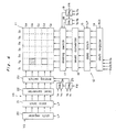
- Fig. 6 shows a driving circuit for a simple matrix type liquid crystal display apparatus of the conventional multiduty adopting a system of reversing the polarities of the picture element data, scanning pulses by the above described alternating signal FR.
- the driving circuit is composed of a segment driver 12 for sequentially outputting one line portion by one line portion the picture element data into the one longitudinal direction of seven line shaped electrode grasping the liquid crystal matrix 11 which composes the thirty five picture elements of 5 X 7, and a common driver 13 for sequentially outputting in a row direction the scanning pulses into the other lateral direction five line shaped electrode grasping above described the liquid crystal.
- the binary (“0",”1") picture element data D1, ..., D7 of seven per line are synchronized with a clock XCK, is accommodated into the shift register 14 of the segment driver 12, and is retained for one horizontal scanning period into a data latch 15 receiving the latch pulse LP.
- a level converter 16 and an analog switch 17 composed of many transistors adjust in level, convert seven input signals of "0” or “1” from the data latch 15 into four operation voltage values V5, V0; V3, V2 to be selected by the voltage value selection switches 18, 19 in accordance with the "H", "L” of the alternating signal FR by on signal, off signal so as to effect parallel output into the one seven line shaped electrodes.
- the shift register 20 of the common driver 13 synchronizes into the latch pulse LP to be inputted for each one horizontal scanning operation the frame scanning start signal YD to be inputted at the scanning start time of one frame so as to shift it.
- the data latch 21 retains the shifted pulse signal for one horizontal scanning period.
- the level converter 22 and the analog switch 23 composed of many transistors adjust in level, convert the five input signals of "0" or "1” from the data latch 21 into four operation voltage values V0, V5; V4, V1 to be selected respectively by the voltage value selection switches 24, 25 in accordance with the "H", "L” of the alternating signal FR from the on signal, off signal so as to effect parallel output into the other five line shaped electrodes.
- the scanning pulses V0, V5 are sequentially scanned from top to bottom like Ca, Cb, ... into the five lateral direction line shaped electrodes by the common driver 13.
- the common driver 13 Among the line liquid crystal with the scanning pulses being fed into it, only the liquid crystal with the white level signals V5, V0 being fed into it bY the segment driver 12 is displayed.
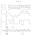
- Fig. 7 is a view showing across a period of two frames the electrode wave forms to be outputted respectively from the above-described analog switches 17, 23 into both electrodes grasping the electrode by way of the liquid crystal of Cb line S2 row on the picture face.
- the frame scanning start signal YD is outputted as a pulse signal into each frame scanning start time.
- the latch pulse LP is outputted five times, setting each horizontal scanning in one frame.
- the D-flip-flop 2 outputs the alternating signal FR which is varied into "H", "L” for each one frame as described hereinabove (see Figs. 4, 5) in accordance with both the pulses.
- the analog switch 17 on the side of the segment driver 12 outputs a black level voltage signal of V3 when the FR is "H” as shown in Fig. 7(d), a black level voltage signal of V2 when the FR is “L”, outputs a white level voltage signal of V5 when the FR is "H”, a white level voltage signal of V0 when the FR is "L".
- the respective No. 2 line, No. 4 line of the first, second frames become white levels.
- the analog switch 23 on the side of the common driver 13 outputs a non-selection level voltage signal of V4 when the FR is the "H", a non-selection level voltage signal of V1 when the FR is the “L”, outputs a selection level voltage signal of V0 when the FR is the "H”, a selection level voltage signal of V5 when the FR is "L”.
- the Cb line becomes the selection level, being set to the second latch pulse LP for a period of scanning the Cb line which is the No. 2 line in the first, second frames. Since the voltage signals like Fig.
- liquid crystal 7 (d), (e) are applied respectively upon both the electrodes grasping the liquid crystal of the Cb line, the S2 row, the potential difference to be added to the liquid crystal is provided as in Fig. 7(f).
- the above described liquid crystal is to light (display) with voltage
- the picture face of the liquid crystal display apparatus becomes larger, and the wave forms of the output voltage signal from both the drivers 12, 13 shown in Fig. 7 (f) become duller when the liquid crystal picture elements to be driven are increased to increase the load.
- the duller wave forms appear considerably (see Fig. 8(c)) when the alternating signal FR changes from the "L” to the “H” or from the "H” to the “L” as shown in Fig. 8(d).
- the output voltage signal from the common driver 13 is much duller. Namely, when the alternating signal FR changes from the "L” to the "H", the non-selection level voltage to be outputted from the common driver 13 changes from V1 to V4. At the same time, after the voltage Ca of the No.
- the black level voltage Lb to be outputted from the segment driver 12 is changed from the V2 to the V3 in accordance with the variation of the FR so as to cause the slight dullness in the wave form corner portion. Therefore, the liquid crystal driving voltage which is the output potential difference of the common driver 13 and the segment driver 12, at the variation time of the alternating signal FR, works in a direction of lowering the potential difference with the dullness of the Ca and the Lb being mutually opposite in direction on the No. 1 line, is not lowered so much in the potential difference with the dullness of the Cb and the Lb being mutually the same in direction on the No. 2 line, works in a direction of increasing the potential difference with the dullness of the Ce and the Lb being opposite in direction on the No.
- the horizontal string shows in the constant value of the turbulent picture face of the effective value of the driving signal affected by the variation in the alternating signal FR, with a defect that the display quality is degraded.
- the present invention has been developed with a view to substantially eliminating the above discussed drawbacks and has for its essential object to provide an improved driving circuit for a liquid crystal display apparatus.
- Another important object of the present invention is to provide a driving circuit for a liquid crystal display apparatus, where the duty of the latch pulses is increased than the number of the actual display lines, the pluraity of the picture element data and the scanning pulse are reversed within the non-display region so as to improve the display quality.
- a driving circuit for a liquid crystal display apparatus which is adapted to sequentially output one line portion of picture element data through the segment driver into one electrode grasping the liquid crystal which becomes the picture elements, sequentially output the scanning pulses in the line direction through the common driver into the other electrode grasping the liquid crystal, and also, reverse for each of the constant periods the polarity of the above described picture element data and the scanning pulse with an alternating signal so as to drive the respective liquid crystal
- the above described common driver is composed of a plurality of drivers cascade connected
- a frame scanning start signal is adapted to be inputted at a time interval corresponding to the latch pulses which are more by few pulses than the number of the actual display lines
- an alternating signal generating means is provided which is adapted to output as the alternating signal into the above described segment driver and the common driver a signal which is delayed at few latch pulse intervals in accordance with the latch pulse of the last line of one frame and is
- the common driver When a first frame scanning start signal is inputted into the common driver, in a case where the alternating signal is, for example, "L", the common driver is synchronized with the latch pulses sequentially from the uppermost stage so as to sequentially output the positive polarity of scanning pulses sequentially from the top into the line shaped electrodes in the line direction of the liquid crystal matrix, at the same time the segment driver is synchronized with the latch pulse to sequentially output in parallel the positive polarity of picture element data of one portion sequentially from the uppermost line into the line shaped electrode of the row direction, each liquid crystal is driven by the positive polarity of voltage which is equivalent to the difference of the above described scanning pulse and the picture element data so as to sequentially light up (display) in the row direction from the uppermost line.
- the pulse signal for the cascade connection use is outputted into the alternating signal generating means from the driver.
- the alternating signal generating means is delayed by a few latch pulse intervals from the input of the above described pulse signal to risingly vary the alternating signal into the "H" to output it into the common driver and the segment driver. Since the next frame scanning start signal is not inputted yet into the common driver although the scanning pulse and picture element data to be outputted respectively from both the drivers are reversed into the reverse polarity, the display of the next frame is not performed by the liquid crystal matrix.
- the next frame scanning start signal is inputted, the liquid crystal matrix is driven sequentially from the uppermost line as described hereinabove by the reverse polarity of voltage corresponding to the difference of the scanning pulse and the picture element data to effect the lighting operation. Since the polarity of the scanning pulse and the picture element data within the non-display region is reversed, the turbulence of the driving voltage accompanied by the reversion does not appear on the display picture face, which does not degrade the display quality.
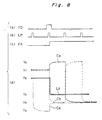
- Fig. 1 a block diagram showing one embodiment of an alternating signal generating circuit to be used in the driving circuit of a liquid crystal display according to one preferred embodiment of the present invention.
- the alternating signal generating circuit has a D-flip-flop 3 provided in the front stage of the NAND gate 1 of the circuit described in Fig. 4.
- a pulse signal Di0 for cascade connection use to be outputted from the common driver to be described is inputted into the reset terminal D
- a latch pulse LP is inputted through the inverter 4 into the set terminal D.
- the output Q of the D-flip-flop 3 is inputted into one input terminal of the NAND gate 1, the above described latch pulse LP is inputted into the other input terminal of the NAND gate 1.
- the above described driving circuit is the same in construction as in Fig. 6, the common driver 13 of the driving circuit described in Fig. 6 is constructed with n number of drivers 6, 6, ... being cascade connected shown as in Fig. 2, with an exception that a period of the frame scanning start signal YD to be inputted into the driver 6 of the uppermost stage is assumed to have the time corresponding to eight latch pulses which are more by three than the number four of the actual display lines Ca through Ce as shown in Fig. 3(a).
- the common driver is synchronized with the latch pulse LP of Fig. 3(c) sequentially from the driver 6 of the uppermost stage with the alternating signal FR being "L" (see Fig. 3 (d)) so as to sequentially output the scanning pulse V0 of the positive polarity sequentially from the top like Ca, cb, ... into five line shaped electrodes in the line direction of the liquid crystal matrix 11.
- the segment driver 12 is synchronized with the latch pulse LP to sequentially output one line portion of the positive polarity of picture elements data V3, V5 sequentially from the uppermost line into seven line shaped electrodes in the row direction.
- the respective liquid crystal is driven with the positive polarity of voltage equivalent to the difference of the scanning pulse and the picture element data so as to sequentially effect the lighting operation from the uppermost line.
- the pulse signal Di0 for the cascade connection is outputted at such a timing as shown in the broken line of Fig. 3(b) from the driver 6 to the D-flip-flop 3 of the alternating signal generating circuit.
- the pulse signal Di0 inputted into the terminal D is latched into the D-flip-flop 3 with the falling of the sixth latch pulse LP, and is inputted into the NAND gate 1 as an output Q delayed by one latch pulse portion as shown in the solid line of Fig. 3(b). Since the NAND gate 1 and the D-flip-flop 2 operate the same operation as in the described in Fig. 5, the alternating signal FR which is the output of the D-flop-flop 2 is caused to be reversed into the "H" with the falling of the seventh latch pulse LP. Thereafter, the eighth latch pulse LP is inputted, the next latch pulse becomes a first latch pulse of the second frame, and at the same time, the second frame scanning start signal YD is inputted as in Fig. 3(a).
- the region becomes an interior N of the non-display display region where the display is not effected on the liquid crystal matrix 11, with the above described quality degraded region M being provided between one latch pulses before and after the reversion of the alternating signal FR within it.
- the same thing can be said about the reversion to the "L” from "H” of the alternating signal FR by the seventh latch pulse of the second frame, with the display quality degradation region M′ by the reversion being also included in the non-display region N′.
- the turbulence of the driving voltage accompanied by the reversion does not show, thus resulting in no degradation in the display quality.
- the pulse signal Di0 for cascade connection use from the lowermost stage of the common driver 5 is used as the trigger signal of the reversion of the alternating signal FR, the circuit for trigger signal generation use is not required to be especially provided.
- the non-display regions N, N′ are made too wide in width, the duty of the latch pulse becomes higher, the effective value difference in driving voltage signal between on and off becomes smaller, so that the contrast of the display becomes worse. It is desired that the latch pulse be restrained into the 2 through 4 latch pulse portions.
- the pulse signal Di0 for cascade connection use is delayed by one latch pulse portion by the use of the D-flip-flop 3, but the pulse signal Di0 may be latched between the one latch pulse on the common driver itself and may be inputted, instead of the frame scanning start signal YD of the NAND gate 1 of Fig. 4.
- a common driver which sequentially drive, output in the row direction the scanning pulses into the other electrode grasping the liquid crystal of a simple matrix type is composed of a plurality of drivers cascade connected.
- the frame canning start signal is inputted, at a time interval corresponding to latch pulses which are more by a few pulses than the number of the actual display lines, into the common driver.
- an alternating signal which is more delayed by a few latch pulse intervals than the latch pulse of the last line of one frame by the alternating signal generating means and is risingly or loweringly varied to generate the alternating signal generating signal so as to output it into the segment driver and the common driver so that the the polarity of the scanning pulse and the picture element data may be reversed within the non-display region. Therefore, the turbulence of the driving voltage accompanied by the reversion does not show on the display picture face, thus resulting in no degradation in the display quality of the liquid display apparatus.
Landscapes
- Engineering & Computer Science (AREA)
- Chemical & Material Sciences (AREA)
- Crystallography & Structural Chemistry (AREA)
- Physics & Mathematics (AREA)
- Computer Hardware Design (AREA)
- General Physics & Mathematics (AREA)
- Theoretical Computer Science (AREA)
- Liquid Crystal Display Device Control (AREA)
- Transforming Electric Information Into Light Information (AREA)
Applications Claiming Priority (2)
| Application Number | Priority Date | Filing Date | Title |
|---|---|---|---|
| JP175252/89 | 1989-07-06 | ||
| JP1175252A JPH0339787A (ja) | 1989-07-06 | 1989-07-06 | 液晶表示装置の駆動回路 |
Publications (3)
| Publication Number | Publication Date |
|---|---|
| EP0406900A2 true EP0406900A2 (de) | 1991-01-09 |
| EP0406900A3 EP0406900A3 (en) | 1992-04-15 |
| EP0406900B1 EP0406900B1 (de) | 1995-02-22 |
Family
ID=15992917
Family Applications (1)
| Application Number | Title | Priority Date | Filing Date |
|---|---|---|---|
| EP90112963A Expired - Lifetime EP0406900B1 (de) | 1989-07-06 | 1990-07-06 | Treiberschaltung für eine Flüssigkristallanzeige |
Country Status (4)
| Country | Link |
|---|---|
| US (1) | US5274366A (de) |
| EP (1) | EP0406900B1 (de) |
| JP (1) | JPH0339787A (de) |
| DE (1) | DE69017101T2 (de) |
Cited By (2)
| Publication number | Priority date | Publication date | Assignee | Title |
|---|---|---|---|---|
| EP0506418A3 (en) * | 1991-03-29 | 1993-07-14 | Oki Electric Industry Company, Limited | Lcd driver circuit |
| EP0529934A3 (en) * | 1991-08-23 | 1993-12-22 | Motorola Inc | Lcd driver and control unit |
Families Citing this family (6)
| Publication number | Priority date | Publication date | Assignee | Title |
|---|---|---|---|---|
| JPH07109544B2 (ja) * | 1991-05-15 | 1995-11-22 | インターナショナル・ビジネス・マシーンズ・コーポレイション | 液晶表示装置並びにその駆動方法及び駆動装置 |
| TW277129B (de) * | 1993-12-24 | 1996-06-01 | Sharp Kk | |
| JP3417514B2 (ja) * | 1996-04-09 | 2003-06-16 | 株式会社日立製作所 | 液晶表示装置 |
| KR100507272B1 (ko) * | 1999-12-29 | 2005-08-10 | 비오이 하이디스 테크놀로지 주식회사 | 박막트랜지스터 액정표시 장치의 스타트 펄스신호 발생 회로 |
| US20050140634A1 (en) * | 2003-12-26 | 2005-06-30 | Nec Corporation | Liquid crystal display device, and method and circuit for driving liquid crystal display device |
| US8836621B2 (en) | 2004-12-15 | 2014-09-16 | Nlt Technologies, Ltd. | Liquid crystal display apparatus, driving method for same, and driving circuit for same |
Family Cites Families (4)
| Publication number | Priority date | Publication date | Assignee | Title |
|---|---|---|---|---|
| US4525710A (en) * | 1982-02-16 | 1985-06-25 | Seiko Instruments & Electronics Ltd. | Picture display device |
| DE3782450T2 (de) * | 1986-04-25 | 1993-03-18 | Seiko Instr Inc | Interface, zum beispiel fuer eine fluessigkristallanzeige. |
| JPH01106017A (ja) * | 1987-10-20 | 1989-04-24 | Seiko Epson Corp | 液晶表示装置の駆動方法 |
| JP2638010B2 (ja) * | 1987-11-30 | 1997-08-06 | カシオ計算機株式会社 | 画像表示装置 |
-
1989
- 1989-07-06 JP JP1175252A patent/JPH0339787A/ja active Pending
-
1990
- 1990-07-03 US US07/547,130 patent/US5274366A/en not_active Expired - Lifetime
- 1990-07-06 DE DE69017101T patent/DE69017101T2/de not_active Expired - Fee Related
- 1990-07-06 EP EP90112963A patent/EP0406900B1/de not_active Expired - Lifetime
Cited By (2)
| Publication number | Priority date | Publication date | Assignee | Title |
|---|---|---|---|---|
| EP0506418A3 (en) * | 1991-03-29 | 1993-07-14 | Oki Electric Industry Company, Limited | Lcd driver circuit |
| EP0529934A3 (en) * | 1991-08-23 | 1993-12-22 | Motorola Inc | Lcd driver and control unit |
Also Published As
| Publication number | Publication date |
|---|---|
| DE69017101D1 (de) | 1995-03-30 |
| JPH0339787A (ja) | 1991-02-20 |
| EP0406900B1 (de) | 1995-02-22 |
| DE69017101T2 (de) | 1995-10-12 |
| EP0406900A3 (en) | 1992-04-15 |
| US5274366A (en) | 1993-12-28 |
Similar Documents
| Publication | Publication Date | Title |
|---|---|---|
| EP0193728B1 (de) | Anzeigesteuersystem | |
| USRE42993E1 (en) | Liquid crystal driver and liquid crystal display device using the same | |
| KR100688498B1 (ko) | 게이트 드라이버가 내장된 액정 패널 및 이의 구동 방법 | |
| CA2065229C (en) | Liquid crystal display apparatus and apparatus for driving it | |
| KR100301545B1 (ko) | 액티브 매트릭스형 액정 표시 장치용 구동 회로 | |
| KR100631112B1 (ko) | 인버젼 방식의 액정패널 구동방법 및 장치 | |
| KR100386128B1 (ko) | 액정디스플레이 및 그 구동방법 | |
| EP0406900A2 (de) | Treiberschaltung für eine Flüssigkristallanzeige | |
| KR950034038A (ko) | 액정표시장치 및 그 구동방법 | |
| JP3169763B2 (ja) | 液晶表示パネルの階調駆動装置 | |
| KR20050071957A (ko) | 액정 표시 장치 및 이의 구동 방법 | |
| EP0371665A1 (de) | Anzeigevorrichtung und Methode zur Steuerung der Anzeige | |
| US5029257A (en) | Method for separating scan line drive in plasma display panel and circuit arrangement thereof | |
| US6121945A (en) | Liquid crystal display device | |
| EP0624862B1 (de) | Steuerungsverfahren für Anzeigevorrichtung | |
| KR930005369B1 (ko) | 많은색의 컬러 표시방법 및 장치 | |
| JP3669514B2 (ja) | 液晶表示装置の駆動回路 | |
| JP2734570B2 (ja) | 液晶表示回路 | |
| KR100486900B1 (ko) | 액정 표시장치 | |
| US5642126A (en) | Driving circuit for driving a display apparatus and a method for the same | |
| EP0447919B1 (de) | Steuereinrichtung für eine Bildpunktmatrixanzeige | |
| EP0599622B1 (de) | Steuerschaltung zur Steuerung einer Anzeigeeinrichtung und Verfahren für dieselbe | |
| JP3549127B2 (ja) | 液晶表示装置 | |
| TWM671564U (zh) | 具局部更新模式的多穩態顯示裝置 | |
| JP3270086B2 (ja) | 液晶表示装置 |
Legal Events
| Date | Code | Title | Description |
|---|---|---|---|
| PUAI | Public reference made under article 153(3) epc to a published international application that has entered the european phase |
Free format text: ORIGINAL CODE: 0009012 |
|
| AK | Designated contracting states |
Kind code of ref document: A2 Designated state(s): DE FR GB |
|
| 17P | Request for examination filed |
Effective date: 19901219 |
|
| PUAL | Search report despatched |
Free format text: ORIGINAL CODE: 0009013 |
|
| AK | Designated contracting states |
Kind code of ref document: A3 Designated state(s): DE FR GB |
|
| 17Q | First examination report despatched |
Effective date: 19931025 |
|
| GRAA | (expected) grant |
Free format text: ORIGINAL CODE: 0009210 |
|
| AK | Designated contracting states |
Kind code of ref document: B1 Designated state(s): DE FR GB |
|
| REF | Corresponds to: |
Ref document number: 69017101 Country of ref document: DE Date of ref document: 19950330 |
|
| ET | Fr: translation filed | ||
| PLBE | No opposition filed within time limit |
Free format text: ORIGINAL CODE: 0009261 |
|
| STAA | Information on the status of an ep patent application or granted ep patent |
Free format text: STATUS: NO OPPOSITION FILED WITHIN TIME LIMIT |
|
| 26N | No opposition filed | ||
| PGFP | Annual fee paid to national office [announced via postgrant information from national office to epo] |
Ref country code: DE Payment date: 20010702 Year of fee payment: 12 |
|
| PGFP | Annual fee paid to national office [announced via postgrant information from national office to epo] |
Ref country code: GB Payment date: 20010704 Year of fee payment: 12 |
|
| PGFP | Annual fee paid to national office [announced via postgrant information from national office to epo] |
Ref country code: FR Payment date: 20010712 Year of fee payment: 12 |
|
| REG | Reference to a national code |
Ref country code: GB Ref legal event code: IF02 |
|
| PG25 | Lapsed in a contracting state [announced via postgrant information from national office to epo] |
Ref country code: GB Free format text: LAPSE BECAUSE OF NON-PAYMENT OF DUE FEES Effective date: 20020706 |
|
| PG25 | Lapsed in a contracting state [announced via postgrant information from national office to epo] |
Ref country code: DE Free format text: LAPSE BECAUSE OF NON-PAYMENT OF DUE FEES Effective date: 20030201 |
|
| GBPC | Gb: european patent ceased through non-payment of renewal fee |
Effective date: 20020706 |
|
| PG25 | Lapsed in a contracting state [announced via postgrant information from national office to epo] |
Ref country code: FR Free format text: LAPSE BECAUSE OF NON-PAYMENT OF DUE FEES Effective date: 20030331 |
|
| REG | Reference to a national code |
Ref country code: FR Ref legal event code: ST |