EP0403972A2 - Circuit amplificateur d'attaque pour charges inductives - Google Patents
Circuit amplificateur d'attaque pour charges inductives Download PDFInfo
- Publication number
- EP0403972A2 EP0403972A2 EP90111326A EP90111326A EP0403972A2 EP 0403972 A2 EP0403972 A2 EP 0403972A2 EP 90111326 A EP90111326 A EP 90111326A EP 90111326 A EP90111326 A EP 90111326A EP 0403972 A2 EP0403972 A2 EP 0403972A2
- Authority
- EP
- European Patent Office
- Prior art keywords
- amplifier
- coupled
- input
- transformer
- primary
- Prior art date
- Legal status (The legal status is an assumption and is not a legal conclusion. Google has not performed a legal analysis and makes no representation as to the accuracy of the status listed.)
- Granted
Links
- 230000001939 inductive effect Effects 0.000 title claims abstract description 29
- 238000004804 winding Methods 0.000 claims abstract description 25
- 238000000034 method Methods 0.000 claims abstract description 12
- 230000000903 blocking effect Effects 0.000 claims 2
- 230000005347 demagnetization Effects 0.000 abstract 1
- 239000003990 capacitor Substances 0.000 description 8
- 230000005415 magnetization Effects 0.000 description 6
- 230000003071 parasitic effect Effects 0.000 description 6
- 230000008901 benefit Effects 0.000 description 5
- 230000001965 increasing effect Effects 0.000 description 4
- 230000006872 improvement Effects 0.000 description 2
- 229920006395 saturated elastomer Polymers 0.000 description 2
- 230000035945 sensitivity Effects 0.000 description 2
- 230000001629 suppression Effects 0.000 description 2
- 239000002699 waste material Substances 0.000 description 2
- 230000009471 action Effects 0.000 description 1
- 238000007792 addition Methods 0.000 description 1
- 230000008859 change Effects 0.000 description 1
- 230000008878 coupling Effects 0.000 description 1
- 238000010168 coupling process Methods 0.000 description 1
- 238000005859 coupling reaction Methods 0.000 description 1
- 230000003247 decreasing effect Effects 0.000 description 1
- 238000007599 discharging Methods 0.000 description 1
- 230000000694 effects Effects 0.000 description 1
- 238000004146 energy storage Methods 0.000 description 1
- 230000006870 function Effects 0.000 description 1
- 230000007246 mechanism Effects 0.000 description 1
- 230000004048 modification Effects 0.000 description 1
- 238000012986 modification Methods 0.000 description 1
- 238000013021 overheating Methods 0.000 description 1
- 230000000737 periodic effect Effects 0.000 description 1
- 230000009467 reduction Effects 0.000 description 1
- 230000004044 response Effects 0.000 description 1
- 230000002441 reversible effect Effects 0.000 description 1
- 230000000630 rising effect Effects 0.000 description 1
- 230000001052 transient effect Effects 0.000 description 1
Images

Classifications
-
- H—ELECTRICITY
- H04—ELECTRIC COMMUNICATION TECHNIQUE
- H04N—PICTORIAL COMMUNICATION, e.g. TELEVISION
- H04N3/00—Scanning details of television systems; Combination thereof with generation of supply voltages
- H04N3/10—Scanning details of television systems; Combination thereof with generation of supply voltages by means not exclusively optical-mechanical
- H04N3/16—Scanning details of television systems; Combination thereof with generation of supply voltages by means not exclusively optical-mechanical by deflecting electron beam in cathode-ray tube, e.g. scanning corrections
- H04N3/18—Generation of supply voltages, in combination with electron beam deflecting
-
- H—ELECTRICITY
- H03—ELECTRONIC CIRCUITRY
- H03K—PULSE TECHNIQUE
- H03K4/00—Generating pulses having essentially a finite slope or stepped portions
- H03K4/06—Generating pulses having essentially a finite slope or stepped portions having triangular shape
- H03K4/08—Generating pulses having essentially a finite slope or stepped portions having triangular shape having sawtooth shape
- H03K4/48—Generating pulses having essentially a finite slope or stepped portions having triangular shape having sawtooth shape using as active elements semiconductor devices
- H03K4/60—Generating pulses having essentially a finite slope or stepped portions having triangular shape having sawtooth shape using as active elements semiconductor devices in which a sawtooth current is produced through an inductor
- H03K4/62—Generating pulses having essentially a finite slope or stepped portions having triangular shape having sawtooth shape using as active elements semiconductor devices in which a sawtooth current is produced through an inductor using a semiconductor device operating as a switching device
- H03K4/64—Generating pulses having essentially a finite slope or stepped portions having triangular shape having sawtooth shape using as active elements semiconductor devices in which a sawtooth current is produced through an inductor using a semiconductor device operating as a switching device combined with means for generating the driving pulses
-
- H—ELECTRICITY
- H03—ELECTRONIC CIRCUITRY
- H03K—PULSE TECHNIQUE
- H03K17/00—Electronic switching or gating, i.e. not by contact-making and –breaking
- H03K17/51—Electronic switching or gating, i.e. not by contact-making and –breaking characterised by the components used
- H03K17/56—Electronic switching or gating, i.e. not by contact-making and –breaking characterised by the components used by the use, as active elements, of semiconductor devices
- H03K17/60—Electronic switching or gating, i.e. not by contact-making and –breaking characterised by the components used by the use, as active elements, of semiconductor devices the devices being bipolar transistors
- H03K17/601—Electronic switching or gating, i.e. not by contact-making and –breaking characterised by the components used by the use, as active elements, of semiconductor devices the devices being bipolar transistors using transformer coupling
Definitions
- the present invention relates to means and methods for power amplifiers and, in particular, power amplifiers capable of driving inductive loads and relatively high repetition rates.
- a power amplifier that is designed to drive inductive loads typically operates as a high-current switching device. Power amplifiers of this type are used, for examples to drive the yoke mechanism of the horizontal deflection circuitry of a display system employing a cathode ray tube (CRT).
- CRT cathode ray tube
- Typical prior art deflection amplifiers are described in U. S. Patents No. 4,670,692, 4,642,533, 4,205,259, 3,501,672 and 3,480,826, which are incorporated herein by reference.
- the switching rate or operating frequency of the deflection amplifier is one factor that determines the degree of resolution of an image formed on the CRT. As the need has increased for progressively higher resolution, so has deflection amplifier operating frequency. Deflection amplifiers operating at 64-270 kHz or higher are now much desired.
- a circuit comprising: amplifying means for driving an inductive load and having a first output terminal coupled to the inductive load, a second output terminal coupled to a common terminal, and an input terminal; an inductor having first and second terminals wherein the first terminal is coupled to the amplifier input terminal; a transformer having primary and secondary windings each having first and second terminals, wherein the first terminal of the primary is coupled to a switch for supplying current to the primary and the second terminal of the primary is coupled to the second terminal of the inductor, and first terminal of the secondary is coupled to the second terminal of the primary and the second terminal of the secondary is coupled through a unidirectional device to the common terminal; and wherein the transformer windings are arranged so that, when the primary is excited, the first terminals of the primary and secondary have the same polarity.
- a further improved circuit for driving an inductive load comprising: amplifying means having a first output terminal coupled to the inductive load, a second output terminal coupled to a common terminals, and an input terminal; an inductor having first and second terminals wherein the first terminal is coupled to the amplifier input terminal; a transformer having primary and secondary windings each having first and second terminals, wherein the first terminal of the primary is coupled to a switch for supplying current to the primary and the second terminal of the primary is coupled to the amplifier input terminal, and first terminal of the secondary is coupled to the second terminal of the inductor and the second terminal of the secondary is coupled through a unidirectional device to the common terminal; and wherein the transformer windings are arranged so that, when the primary is excited, the first terminals of the primary and secondary have the same polarity.
- an improved method for driving an inductive load coupled to the output of an amplifying means whose input is coupled to a transformer primary and secondary through an inductor comprising: energizing the input of the amplifier through the primary circuit coupled to the amplifier input through the inductor while the secondary circuit of the same transformer coupled to the same amplifier input through the same inductor is substantially blocked from conducting, and thereafter de-energizing the amplifier input through the inductor and transformer secondary while the transformer primary circuit is substantially blocked from conducting.
- a further improved method for driving an inductive load coupled to the output of an amplifying means whose input is coupled directly to a transformer primary and coupled to the transformer secondary through an inductor comprising: energizing the input of the amplifier through the primary circuit coupled to the amplifier input while the secondary circuit of the same transformer coupled to the same amplifier input through the inductor is substantially blocked from conducting, and thereafter de-energizing the amplifier input through the inductor and transformer secondary while the transformer primary circuit is substantially blocked from conducting.
- Prior art CRT horizontal deflection amplifier circuit 10 shown in FIG. 1, comprises input power supply connection 11, current limiting resistor 12, switch 14, transformer 16 having primary winding 18 and secondary winding 20, series inductor 22, shunt resistor 24, amplifier 26, snubber diode 28, energy storage capacitor 30 and deflection coil 32.
- Power supply connection 13 is provided for forcing a current through coil 32 and charging capacitor 30 in response to whether amplifier 32 is conducting or not.
- Common connection 15 is also provided.
- Switch 14 may be any type of rapidly operating switch well known in the art for providing an interruptible current path to power supply connection 11. For CRT deflection applications, switch 14 usually operates in a periodic manner with a switching frequency equal to the desired deflection frequency.
- Amplifier 26 is typically a high power bipolar transistor, but other amplifying devices and circuits may also be used, as for example, power MOSFETS, Darlingtons and/or BiMOS devices or circuits.
- amplifier is intended to refer to these and other alternatives as will occur to those of skill in the art based on the disclosure herein.
- the operation of circuit 10 is described using a bipolar type transistor as amplifier 26, however, the principles of operation apply to other amplifiers as well.
- inductor 22 is in series with the input of amplifier 26 during both the turn-on and turn-off portions of the deflection drive cycle.
- inductor 22 adds impedance to the input drive circuit, thereby requiring that larger drive voltages be provided through switch 14.
- the series resistance of inductor 22 adds to the power loss in the circuit during turn-on.
- the energy stored in inductor 22 during the turn-on portion of the amplifier input drive opposes the oppositely directed base current flow during the turn-off portion of the input drive cycle, thereby making it more difficult to turn off amplifier 26.
- turn-on current 25 and turn-off current 27 are not independently controllable. Also, substantial power is dissipated in current limiting resistor 12.
- the relatively square base input current (i b ) pulse shape during turn-on increases the charge stored in the amplifier which must be extracted during turn-off and increases the power dissipated in amplifier 26.
- the operation of the circuit of FIG. 1 is relatively sensitive to variation in amplifier characteristics. These are significant problems.
- FIG. 2 shows inductive load drive circuit 40, according to a first embodiment of the present invention.
- Circuit 40 comprises input switching device 44 analogous to switch 14 of FIG. 1, parasitic suppression resistor 42, transformer 46 having primary 48 and secondary 50, inductor 52, amplifier means 26, e.g., a bipolar transistor, resistor 54 and unidirectional conducting means 56, e.g., a diode or equivalent, coupled substantially as shown.
- Deflection coil 32, diode 28, capacitor 30 and power connections 11 and 13 and reference connection 15 are the same as in FIG. 1.
- Primary 48 and secondary 50 of transformer 46 have the indicated polarity relationship, i.e., the black dots adjacent the windings indicating the ends of the windings having the same polarity when, for example, the primary is excited.
- transformer 46 acts as an inductor having an inductance determined by primary winding 48 which provides primary control of the rate of rise of input drive current 45.
- control over input current and amplifier turn-on is improved by virtue of the ability to separately select the primary inductance.
- the presence of diode 56 prevents transformer action during the turn-on portion of the input drive to amplifier 26.
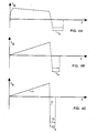
- FIG. 4B shows the direction and relative magnitude of the amplifier input current versus time for the circuit of FIG. 2. It will be seen that a positive going ramp is obtained during amplifier input turn-on and a negative going saturated ramp is obtained during turn-off. Further, because the shape of the turn-on portion is primarily controlled by the inductance of primary winding 48 and the shape of the turn-off portion is primarily determined by the inductance of inductor 52, the ability to separately control the turn-on and turn-off portions of the amplifier input drive is improved. Further, the saturated portion of the turn-off input drive may be adjusted by selecting the turns ratio of transformer 46, providing additional control over operation of the power amplifier.
- FIG. 4C A further improved circuit is shown in FlG. 3, which is preferred.
- the waveform associated with the amplifier input drive current 65, 67 of the circuit of FlG. 3 is shown in FIG. 4C.
- Drive circuit 60 of FIG. 3 is similar to that of FIG.2 and has substantially the same components, except that primary winding 48 is coupled to the input of amplifier 26 without passing through inductor 52.
- the operation of circuit 60 of FlG. 3 differs from that of circuit 40 of FIG. 2 in that, during input turn-on when switch 44 is closed, input current 65 flows through primary winding 48 into the input of amplifier 26 without passing through inductor 52.
- transformer 46 functions as an inductor determined by the inductance of primary winding 48.
- the rate of rise of the input drive current during the turn-on portion of the amplifier input may be substantially independently selected by choosing the inductance of primary 48. It should also be noted that there is no series resistance in the input circuit other than the parasitic resistance of the transformer primary and circuit wiring, which may be made relatively small. The series resistance of inductor 52 is not in the circuit during turn-on. Thus, power dissipation is reduced.
- a further advantage of the circuit of FIG. 3 is that the energy which was previously stored in inductor 52 in the circuits of FIGS. 1-2, and which opposed removal of the charge stored in the input of amplifier 26 and which was wasted, is no longer present.
- This energy is given by 1/2 L52[I(25) peak ]2 or 1/2 L52[I(45) peak ]2, where L52 stands for the inductance of inductor 52 and I(25) peak and I(45) peak indicate the peak values of turn-on input charging currents 25 and 45, respectively.
- L52 stands for the inductance of inductor 52
- I(25) peak and I(45) peak indicate the peak values of turn-on input charging currents 25 and 45, respectively.
- the magnitude of the circuit components may be arranged so that the energy needed to turn off amplifier 26 is provided by the energy stored in primary winding 48 of transformer 46 substantially independent of the other components.
- This stored energy is 1/2 L p [I(65) peak ]2, where L p stands for the inductance of primary winding 48 of transformer 46 and I(65) peak stands for the peak value of turn-on input charging current 65.
- L p stands for the inductance of primary winding 48 of transformer 46
- I(65) peak stands for the peak value of turn-on input charging current 65.
- the amount of energy needed to turn-off amplifier 26 is frequently substantial.
- the input drive is substantially lossless. This is a great advantage.
- an amplifier drive circuit suitable for driving inductive loads such as are encountered in CRT horizontal deflection is implemented with voltage of typically 6 volts at power supply connection, resistor 42 of 470 Ohms (1 Watt), transformer 46 of Type 1811P-3C8 manufactured by Feroxcube of Saugerties. NY with a turns ration of about 12:4 and primary inductance of 50 microHenries, inductor 52 of about 2 microHenries, resistor 54 of about 22 Ohms (1 Watt), diode 56 of Motorola Type MUR110 rectifier and amplifier 26 of Motorola Type MJH16206 bipolar transistor manufactured by Motorola, Inc. of Phoenix, AZ. Other components are conventional.
- the voltage of supply connection 13 and output components 28, 30, are chosen depending upon the desired properties of deflection coil 32 using means well known in the art.
- FIGS, 1-3 were compared using the same amplifier transistor and operating at the same frequencies under substantially the same conditions. Three important parameters are considered; the storage time t s (see FlGS. 4A-C) during which the charge stored in the amplifier is being extracted, the switching power loss (SWPL) in the circuit and the variation ⁇ t f in collector current fall time t f observed due to variations in individual transistor characteristics.
- the results are presented in the following table, normalized to the behavior of the circuit of FlG. 1.
- the reduction in ⁇ t f is extremely important because it indicates that the invented circuits are much more tolerant of unavoidable device characteristic variations. This is greatly to be desired.
- the invented circuit and method provide substantial improvement over the prior art by increasing the degree of freedom in independently setting the input operation of the amplifier for driving inductive loads during amplifier input turn-on, turn-off and turn-off saturation, that power dissipation is substantially reduced, and that the sensitivity to variations in transistor characteristics is much reduced.
- the invented means and method are especially well suited for driving inductive loads such as are encountered in high speed CRT deflection power amplifiers,
Landscapes
- Engineering & Computer Science (AREA)
- Power Engineering (AREA)
- Multimedia (AREA)
- Signal Processing (AREA)
- Amplifiers (AREA)
- Details Of Television Scanning (AREA)
- Electronic Switches (AREA)
Applications Claiming Priority (2)
| Application Number | Priority Date | Filing Date | Title |
|---|---|---|---|
| US07/369,413 US4897580A (en) | 1989-06-20 | 1989-06-20 | Amplifier drive circuit for inductive loads |
| US369413 | 1989-06-20 |
Publications (3)
| Publication Number | Publication Date |
|---|---|
| EP0403972A2 true EP0403972A2 (fr) | 1990-12-27 |
| EP0403972A3 EP0403972A3 (fr) | 1991-09-25 |
| EP0403972B1 EP0403972B1 (fr) | 1995-01-25 |
Family
ID=23455380
Family Applications (1)
| Application Number | Title | Priority Date | Filing Date |
|---|---|---|---|
| EP90111326A Expired - Lifetime EP0403972B1 (fr) | 1989-06-20 | 1990-06-15 | Circuit amplificateur d'attaque pour charges inductives |
Country Status (5)
| Country | Link |
|---|---|
| US (1) | US4897580A (fr) |
| EP (1) | EP0403972B1 (fr) |
| JP (1) | JPH07118777B2 (fr) |
| KR (1) | KR0149668B1 (fr) |
| DE (1) | DE69016272T2 (fr) |
Cited By (3)
| Publication number | Priority date | Publication date | Assignee | Title |
|---|---|---|---|---|
| EP0520331A2 (fr) * | 1991-06-24 | 1992-12-30 | Nokia (Deutschland) GmbH | Circuit de déviation horizontale avec un transformateur de commande |
| WO1997004526A1 (fr) * | 1995-07-21 | 1997-02-06 | Apple Computer, Inc. | Procede et appareil de commande d'etages de deviation et de haute tension dans un affichage video |
| EP0786866A1 (fr) * | 1996-01-25 | 1997-07-30 | Deutsche Thomson-Brandt Gmbh | Circuit de commande pour un transistor de commutation déclenché périodiquement |
Families Citing this family (2)
| Publication number | Priority date | Publication date | Assignee | Title |
|---|---|---|---|---|
| US5352462A (en) * | 1982-06-03 | 1994-10-04 | Stolle Research & Development Corporation | Anti-inflammatory factor, method of isolation, and use |
| US6107860A (en) * | 1991-12-11 | 2000-08-22 | Vlt Corporation | High efficiency floating gate driver circuit using leakage-inductance transformer |
Citations (4)
| Publication number | Priority date | Publication date | Assignee | Title |
|---|---|---|---|---|
| FR2382134A1 (fr) * | 1977-02-28 | 1978-09-22 | Thorn Automation Ltd | Perfectionnements a un etage de puissance a transistors |
| SU636802A1 (ru) * | 1977-03-30 | 1978-12-05 | Glebov Boris A | Устройство управлени транзистором |
| US4642533A (en) * | 1985-03-27 | 1987-02-10 | Ocean Technology, Inc. | Constant current power circuit for horizontal deflection of cathode ray tube |
| US4670692A (en) * | 1984-09-17 | 1987-06-02 | Tektronix, Inc. | High-speed power amplifier for driving inductive loads |
Family Cites Families (4)
| Publication number | Priority date | Publication date | Assignee | Title |
|---|---|---|---|---|
| US3480826A (en) * | 1968-10-25 | 1969-11-25 | Gen Electric | Television receiver horizontal sweep circuit having protection against arcing |
| US3501672A (en) * | 1968-10-25 | 1970-03-17 | Gen Electric | Drive for television receiver horizontal sweep circuit output transistor |
| DE2809378A1 (de) * | 1978-03-04 | 1979-09-13 | Blaupunkt Werke Gmbh | Horizontalablenkschaltung |
| US4227123A (en) * | 1979-02-12 | 1980-10-07 | Rca Corporation | Switching amplifier for driving a load through an alternating-current path with a constant-amplitude, varying duty cycle signal |
-
1989
- 1989-06-20 US US07/369,413 patent/US4897580A/en not_active Expired - Fee Related
-
1990
- 1990-06-14 JP JP2154176A patent/JPH07118777B2/ja not_active Expired - Fee Related
- 1990-06-15 DE DE69016272T patent/DE69016272T2/de not_active Expired - Fee Related
- 1990-06-15 EP EP90111326A patent/EP0403972B1/fr not_active Expired - Lifetime
- 1990-06-15 KR KR1019900008795A patent/KR0149668B1/ko not_active IP Right Cessation
Patent Citations (4)
| Publication number | Priority date | Publication date | Assignee | Title |
|---|---|---|---|---|
| FR2382134A1 (fr) * | 1977-02-28 | 1978-09-22 | Thorn Automation Ltd | Perfectionnements a un etage de puissance a transistors |
| SU636802A1 (ru) * | 1977-03-30 | 1978-12-05 | Glebov Boris A | Устройство управлени транзистором |
| US4670692A (en) * | 1984-09-17 | 1987-06-02 | Tektronix, Inc. | High-speed power amplifier for driving inductive loads |
| US4642533A (en) * | 1985-03-27 | 1987-02-10 | Ocean Technology, Inc. | Constant current power circuit for horizontal deflection of cathode ray tube |
Non-Patent Citations (1)
| Title |
|---|
| SOVIET INVENTIONS ILLUSTRATED, week B37, 24th October 1979, Section H, Class R55, accession no. 467532 (2 pp. 138), Derwent Publications Ltd, London, GB; & SU-A-636 802 (GLEBOV) 05-12-1978 * |
Cited By (5)
| Publication number | Priority date | Publication date | Assignee | Title |
|---|---|---|---|---|
| EP0520331A2 (fr) * | 1991-06-24 | 1992-12-30 | Nokia (Deutschland) GmbH | Circuit de déviation horizontale avec un transformateur de commande |
| EP0520331A3 (en) * | 1991-06-24 | 1993-02-10 | Nokia (Deutschland) Gmbh | Horizontal deflection circuit with a driving transformer |
| WO1997004526A1 (fr) * | 1995-07-21 | 1997-02-06 | Apple Computer, Inc. | Procede et appareil de commande d'etages de deviation et de haute tension dans un affichage video |
| EP0786866A1 (fr) * | 1996-01-25 | 1997-07-30 | Deutsche Thomson-Brandt Gmbh | Circuit de commande pour un transistor de commutation déclenché périodiquement |
| CN1055182C (zh) * | 1996-01-25 | 2000-08-02 | 德国汤姆逊-布朗特公司 | 周期性启动开关晶体管的控制电路 |
Also Published As
| Publication number | Publication date |
|---|---|
| KR910002225A (ko) | 1991-01-31 |
| US4897580A (en) | 1990-01-30 |
| JPH0332282A (ja) | 1991-02-12 |
| EP0403972B1 (fr) | 1995-01-25 |
| JPH07118777B2 (ja) | 1995-12-18 |
| EP0403972A3 (fr) | 1991-09-25 |
| DE69016272T2 (de) | 1995-09-07 |
| DE69016272D1 (de) | 1995-03-09 |
| KR0149668B1 (ko) | 1998-10-15 |
Similar Documents
| Publication | Publication Date | Title |
|---|---|---|
| US4365171A (en) | Low loss snubber circuit | |
| US4302807A (en) | Controlled current base drive circuit | |
| EP1235334B1 (fr) | Circuit d'attaque de gachette pour thyristor | |
| JP3260036B2 (ja) | 電圧駆動形電力用スイッチ素子のゲート駆動回路 | |
| US5107190A (en) | Means and method for optimizing the switching performance of power amplifiers | |
| EP0649214A2 (fr) | Régulateur à découpage de haut rendement | |
| US4918569A (en) | Regulated forward converter for generating repeating spark discharge pulses | |
| JP2588594B2 (ja) | 水平偏向回路 | |
| EP0403972B1 (fr) | Circuit amplificateur d'attaque pour charges inductives | |
| US4519023A (en) | Self-oscillating inverter including a DC to DC converter and method for control thereof | |
| JPH0723248A (ja) | 偏向回路 | |
| US6144193A (en) | Isolated transformer coupled gate drive for signals having variable duty cycle | |
| JPH05252409A (ja) | 高電圧発生回路 | |
| US4472662A (en) | Deflection circuit | |
| KR890004210B1 (ko) | 구동 회로(驅動回路) | |
| CN113765510A (zh) | 一种晶闸管驱动电路 | |
| JP2781917B2 (ja) | テレビジョン受像機用電源 | |
| US4721922A (en) | Electric signal amplifiers | |
| JP2870945B2 (ja) | 誘導加熱調理器 | |
| JPH0568891B2 (fr) | ||
| US4864247A (en) | High speed base drive for power amplifier | |
| EP0504687A2 (fr) | Arrangement de rétroaction dans un circuit de déflection | |
| JPH09246935A (ja) | 周期的に操作されるスイッチングトランジスタ用制御回路 | |
| JP3646373B2 (ja) | 高周波偏向回路 | |
| JP3507638B2 (ja) | サイリスタ式パルス放電回路 |
Legal Events
| Date | Code | Title | Description |
|---|---|---|---|
| PUAI | Public reference made under article 153(3) epc to a published international application that has entered the european phase |
Free format text: ORIGINAL CODE: 0009012 |
|
| AK | Designated contracting states |
Kind code of ref document: A2 Designated state(s): DE FR GB IT |
|
| PUAL | Search report despatched |
Free format text: ORIGINAL CODE: 0009013 |
|
| AK | Designated contracting states |
Kind code of ref document: A3 Designated state(s): DE FR GB IT |
|
| 17P | Request for examination filed |
Effective date: 19911118 |
|
| 17Q | First examination report despatched |
Effective date: 19940420 |
|
| GRAA | (expected) grant |
Free format text: ORIGINAL CODE: 0009210 |
|
| ITF | It: translation for a ep patent filed | ||
| AK | Designated contracting states |
Kind code of ref document: B1 Designated state(s): DE FR GB IT |
|
| REF | Corresponds to: |
Ref document number: 69016272 Country of ref document: DE Date of ref document: 19950309 |
|
| ET | Fr: translation filed | ||
| PLBE | No opposition filed within time limit |
Free format text: ORIGINAL CODE: 0009261 |
|
| STAA | Information on the status of an ep patent application or granted ep patent |
Free format text: STATUS: NO OPPOSITION FILED WITHIN TIME LIMIT |
|
| 26N | No opposition filed | ||
| PGFP | Annual fee paid to national office [announced via postgrant information from national office to epo] |
Ref country code: GB Payment date: 19980401 Year of fee payment: 9 |
|
| PGFP | Annual fee paid to national office [announced via postgrant information from national office to epo] |
Ref country code: FR Payment date: 19980407 Year of fee payment: 9 |
|
| PGFP | Annual fee paid to national office [announced via postgrant information from national office to epo] |
Ref country code: DE Payment date: 19980423 Year of fee payment: 9 |
|
| PG25 | Lapsed in a contracting state [announced via postgrant information from national office to epo] |
Ref country code: GB Free format text: LAPSE BECAUSE OF NON-PAYMENT OF DUE FEES Effective date: 19990615 |
|
| PG25 | Lapsed in a contracting state [announced via postgrant information from national office to epo] |
Ref country code: FR Free format text: THE PATENT HAS BEEN ANNULLED BY A DECISION OF A NATIONAL AUTHORITY Effective date: 19990630 |
|
| GBPC | Gb: european patent ceased through non-payment of renewal fee |
Effective date: 19990615 |
|
| PG25 | Lapsed in a contracting state [announced via postgrant information from national office to epo] |
Ref country code: DE Free format text: LAPSE BECAUSE OF NON-PAYMENT OF DUE FEES Effective date: 20000503 |
|
| REG | Reference to a national code |
Ref country code: FR Ref legal event code: ST |
|
| PG25 | Lapsed in a contracting state [announced via postgrant information from national office to epo] |
Ref country code: IT Free format text: LAPSE BECAUSE OF NON-PAYMENT OF DUE FEES;WARNING: LAPSES OF ITALIAN PATENTS WITH EFFECTIVE DATE BEFORE 2007 MAY HAVE OCCURRED AT ANY TIME BEFORE 2007. THE CORRECT EFFECTIVE DATE MAY BE DIFFERENT FROM THE ONE RECORDED. Effective date: 20050615 |