EP0385482A2 - In einer integrierten MOS-Logikschaltung verwendete Eingangsschalteinrichtung - Google Patents
In einer integrierten MOS-Logikschaltung verwendete Eingangsschalteinrichtung Download PDFInfo
- Publication number
- EP0385482A2 EP0385482A2 EP90104036A EP90104036A EP0385482A2 EP 0385482 A2 EP0385482 A2 EP 0385482A2 EP 90104036 A EP90104036 A EP 90104036A EP 90104036 A EP90104036 A EP 90104036A EP 0385482 A2 EP0385482 A2 EP 0385482A2
- Authority
- EP
- European Patent Office
- Prior art keywords
- input
- signal
- whose
- supplied
- node
- Prior art date
- Legal status (The legal status is an assumption and is not a legal conclusion. Google has not performed a legal analysis and makes no representation as to the accuracy of the status listed.)
- Granted
Links
Images


Classifications
-
- H—ELECTRICITY
- H03—ELECTRONIC CIRCUITRY
- H03K—PULSE TECHNIQUE
- H03K17/00—Electronic switching or gating, i.e. not by contact-making and –breaking
-
- H—ELECTRICITY
- H03—ELECTRONIC CIRCUITRY
- H03K—PULSE TECHNIQUE
- H03K19/00—Logic circuits, i.e. having at least two inputs acting on one output; Inverting circuits
- H03K19/02—Logic circuits, i.e. having at least two inputs acting on one output; Inverting circuits using specified components
- H03K19/173—Logic circuits, i.e. having at least two inputs acting on one output; Inverting circuits using specified components using elementary logic circuits as components
- H03K19/1733—Controllable logic circuits
- H03K19/1735—Controllable logic circuits by wiring, e.g. uncommitted logic arrays
- H03K19/1736—Controllable logic circuits by wiring, e.g. uncommitted logic arrays in which the wiring can be modified
-
- H—ELECTRICITY
- H03—ELECTRONIC CIRCUITRY
- H03K—PULSE TECHNIQUE
- H03K17/00—Electronic switching or gating, i.e. not by contact-making and –breaking
- H03K17/51—Electronic switching or gating, i.e. not by contact-making and –breaking characterised by the components used
- H03K17/56—Electronic switching or gating, i.e. not by contact-making and –breaking characterised by the components used by the use, as active elements, of semiconductor devices
- H03K17/687—Electronic switching or gating, i.e. not by contact-making and –breaking characterised by the components used by the use, as active elements, of semiconductor devices the devices being field-effect transistors
- H03K17/693—Switching arrangements with several input- or output-terminals, e.g. multiplexers, distributors
Definitions
- the present invention relates to an input switching device used in a logic MOS integrated circuit.
- a conventional input switching device comprises a register, a first and second logic circuits, and a first and second flag circuits.
- the register receives an arbitrary input signal and then stores it.
- the first logic circuit is supplied with the input signal and data stored in the register.
- the first logic circuit is controlled in accordance with the condition of a flag of the first flag circuit and outputs one of the input signal and the data stored in the register.
- the second logic circuit is supplied with an input signal from an input pad of an integrated circuit.
- the second logic circuit supplies the input signal from the input pad to a clock input terminal of the register in accordance with the condition of a flag of the second flag circuit to thereby control the operation of the register or supplies the input signal from the input pad to peripheral circuit as an input signal.
- the input signal supplied from the input pad is selectively used as a clock signal for controlling the operation of the register and an input signal of the peripheral circuit.
- This circuit arrangement aims at reducing the number of IC pads by using the input pad for both inputting clock signals and inputting signals to the peripheral circuit.
- the first logic circuit comprises a first and second AND gates and a OR gate.
- the above-described arbitrary input signal is supplied to one input terminal of the first AND gate, and an output signal of the register is supplied to one input terminal of the second AND gate.
- An inverted signal of an output signal of the first flag circuit is supplied to the other input terminal of the first AND gate, and an output signal of the first flag circuit is supplied to the other input terminal of the second AND gate.
- Output signals of the first and second AND gates are supplied to an OR gate, and the arbitrary input signal or the data stored in the register is output from an output terminal of the OR gate in accordance with the flag of the first flag circuit.
- the second logic circuit comprises a third and fourth AND gates.
- An output signal of the second flag circuit is supplied to one input terminal of the third AND gate and its inverted signal is supplied to the other input terminal of the fourth AND gate.
- Input signals are supplied from the input pads to the other input terminals of the third and fourth AND gates.
- An output signal of the third AND gate is supplied to the clock input terminal of the register, and an output signal of the fourth AND gate is supplied to the peripheral circuit as an input signal.
- Another object of this invention is to provide an input switching device capable of preventing high power consumption.
- Still another object of this invention is to provide an input switching device which can be operated by a single flag circuit and which can simplify a flag setting operation and reduce the area of a pattern.
- an input switching device comprising: a logic circuit whose operation is controlled by a control signal, for performing logical processing in response to a first input signal; a first selector circuit for receiving the first input signal and an output signal of the logic circuit, and selecting and outputting one of the first input signal and the output signal; a second selector circuit for selecting one of supplying a second input signal to the logic circuit as a control signal and supplying the second input signal to a peripheral circuit as an input signal; and a control circuit for controlling selecting operations of the first and second selector circuits to supply the second input signal to the logic circuit as a control signal when the first selector circuit selects the output signal of the logic circuit and to supply the second input signal to the peripheral circuit as an input signal when the first selector circuit selects the first input signal.
- two selector circuits are controlled by one flag circuit (control circuit) and the selecting operation of the first selector circuit is associated with that of the second selector circuit.
- the second selector circuit supplies the second input signal to the register (logic circuit) as a clock signal and thus the register goes into an operation state. Consequently, any malfunction does not occur and a reliable operation can be expected.
- the second selector circuit When the first selector circuit selects and outputs the first input signal, the second selector circuit outputs the second input signal as an input signal of the peripheral circuit. Since the register is not supplied with a clock signal for control, it is not operated. Low power consumption can be achieved without wasting power consumption.
- the flag setting operation can be simplified and the area of a pattern can be decreased.
- Fig. 1 shows an input switching device according to a first embodiment of the present invention.
- the input switching device comprises register 1 (logic means), first and second logic circuits (first and second selector means) 2 and 3, and flag circuit (control means) 21.
- Register 1 is supplied with arbitrary input signal (first input signal 6.
- Logic circuit 2 is supplied with input signal 6 and data 7 stored in register 1.
- Logic circuit 2 comprises AND gates 23 and 24 and OR gate 25. Input signal 6 is supplied to one of input terminals of AND gate 23 and data 7 stored in register 7 is supplied to one of input terminals of AND gate 24.
- Output signal 12 of flag circuit 21 is inverted and supplied to the other input terminal of AND gate 23, and output signal 12 of flag circuit 21 is supplied to the other input terminal of AND gate 24.
- Output signals of AND gates 23 and 24 are supplied to OR gate 25, and output signal 11 is output from an output terminal of OR gate 25 via output pad 28.
- Logic circuit 2 is controlled in accordance with the condition of the flag set in flag circuit 21, selects one of input signal 6 and stored data 7, and outputs a selected one as output signal 11.
- Logic circuit 3 is supplied with input signal 10 (second input signal) supplied from input pad 22 of an IC.
- Logic circuit 3 comprises AND gates 26 and 27.
- Output signal 12 of flag circuit 21 is supplied to one of input terminals of AND gate 26, and an inverted signal of signal 12 is supplied to one of input terminals of AND gate 27.
- Input signal 10 is supplied to the other input terminals of AND gates 26 and 27.
- Output signal 8 of AND gate 26 is supplied to a clock input terminal of register 1, and output signal 9 of AND gate 27 is supplied to a peripheral circuit as an input signal.
- Logic circuit 3 supplies input signal 10 to the clock input terminal of register 1 as clock signal 8 in accordance with the setting state of the flag of flag circuit 21, and controls the operation of register 1 or supplies output signal 9 of logic circuit 3 to the peripheral circuit as an input signal.
- Fig. 2 shows an example of the structure of register 1 in the device shown in Fig. 1.
- Regster 1 comprises two clocked inverters 29 and 30 controlled by clock signal 8 and inverter 31.
- Input signal 6 is supplied to an input node of clocked inverter 29.
- An output node of clocked inverter 29 is connected to an input node of inverter 31 and an output node of clocked inverter 30.
- An output node of inverter 31 is connected to an input node of clocked inverter 30.
- Stored data 7 is output from the output node of inverter 31.
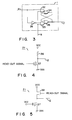
- FIG. 3 shows another example of the structure of register 1 of the device shown in Fig. 1.
- Register 1 comprises two AND gates 32 and 33, two NOR gates 34 and 35, and inverter 36.
- Input signal 6 is supplied to one of input terminals of AND gate 32 and an input node of inverter 36.
- An output signal of inverter 36 is supplied to one of input terminals of AND gate 33.
- Clock signal 8 is supplied from AND gate 26 to the other input terminals of AND gates 32 and 33.
- An output signal of AND gate 32 is supplied to one of input terminals of NOR gate 34, and an output signal of AND gate 33 is supplied to one of input terminals of NOR gate 35.
- An output signal of NOR gate 35 is supplied to the other input terminal of NOR gate 34, and an output signal of NOR gate 34 is supplied to the other input terminal of NOR gate 35.
- Stored data 7 is output from an output terminal of NOR gate 35.
- Fig. 4 illustrates an example of the structure of flag circuit 21 of the device shown in Fig. 1.
- Flag circuit 21 comprises EPROM cell 37 and load element 38.
- a current path of resistor 38 serving as the load element and EPROM cell 37 is connected in series between power source Vcc and ground Vss.
- a read-out signal is supplied to a control gate of EPROM cell 37.
- Signal 12 is output from a connecting node of resistor 38 and EPROM 37.
- flag circuit 21 illustrated in Fig. 4 when a floating gate of EPROM cell 37 is charged with electrons, cell 37 is not turned on even if a read-out signal is supplied. Output signal 12 of flag circuit 12 is thus set at an "H" (high) level. When the floating gate is not charged with electrons, a read-out signal is supplied and then cell 37 is turned on. Output signal 12 of flag circuit 12 is set at an "L" (low) level.
- MOS transistor 39 can be used as a load element in place of resistor 38, and the conducting state of transistor 39 can be controlled by a read-out signal.
- Power source voltage Vcc is applied to the control gate of EPROM cell 37.
- Flag circuit 21 is not limited to the structures shown in Figs. 4 and 5 and it only has to be so constructed that the level of output signal 12 can be switched to an "H" level or an "L" level.
- first logic circuit 2 selects and outputs data 7 stored in register 1
- second logic circuit 3 supplies input signal 10 to register 1 as clock signal 8 and thus register 1 goes into an operating state. Consequently, any malfunction does not occur.
- first logic circuit 2 selects and outputs input signal 6
- second logic circuit 3 always outputs input signal 10 as input signal 9 of the peripheral circuit. Since register 1 is not supplied with a clock signal for control, it is not operated. Low power consumption can be achieved without wasting power consumption. Furthermore, since the number of flag circuits is one, the flag setting operation can be simplified and the area of a pattern can be decreased.
- Fig. 6 shows an input switching device according to a second embodiment of the present invention, which includes a plurality of the circuits ( n circuits.
- the device shown in Fig. 6 comprises circuit blocks 40-1 to 40-n including register 1, logic circuit 2 and output pad 28 shown in Fig. 1.
- Circuit block 40-1 is controlled by flag circuit 21-1.
- circuit blocks 40-2 to 40-n are controlled by flag circuits 21-2 to 21-n, respectively.
- Output signals 12-1 to 12-n of flag circuits 21-1 to 21-n are supplied to an input terminal of n input OR gate 41 arranged in logic circuit 3′.
- An output signal of OR gate 41 is supplied to one of input terminals of AND gate 26, and its inverted signal is supplied to one of input terminals of AND gate 27.
- Input signal 10 is supplied from input pad 22 to the other input terminals of AND gates 26 and 27.
- Output signal 8 of AND gate 26 is supplied to the clock input terminals of registers 1-1 to 1-n arranged in circuit blocks 40-1 to 40-n.
- Output signal 9 of AND gate 27 is supplied to an input terminal of a peripheral circuit (not shown).
- logic circuit 3′ allows and prevents the supply of a minimum essential clock signal in accordance with the selecting operations of logic circuits 2-1 to 2-n; accordingly, an input switching operation can be reliably and satisfactorily operated.
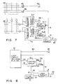
- Fig. 7 shows a circuit arrangement in which the circuit shown in Fig. 1 is applied to a system.
- An input signal supplied to IC input pad 42 is supplied to an input terminal of buffer circuit 43.
- Buffer circuit 43 comprises a main output terminal and an inversion output terminal.
- An output signal of buffer circuit 43 is supplied to first memory matrix 44.
- An output signal of memory matrix 44 is supplied to second memory matrix 45.
- An output signal of memory matrix 45 is supplied to data input terminals of registers 1-1 and 1-2 and to logic circuits 2-1 and 2-2.
- Data stored in register 1-1 is supplied to logic circuit 2-1, and data stored in register 1-2 is supplied to logic circuit 2-2.
- Output signal 11-1 of logic circuit 2-1 is output from output pad 28-1, and output signal 11-2 of logic circuit 2-2 is output from output pad 28-2.
- Input signal 10 supplied to input pad 22 is supplied to logic circuit 3′.
- Logic circuit 3′ has basically the same arrangement as that of logic circuit 3′ shown in Fig. 6 and its output signal 9 is supplied to buffer circuit 46.
- Buffer circuit 46 comprises a main output terminal and an inversion output terminal as buffer circuit 43 does, and its output signal is supplied to registers 1-1 and 1-2 and logic circuits 2-1 and 2-2 via first and second memory matrices 44 and 45.
- Output signal 8 of logic circuit 3′ is supplied to registers 1-1 and 1-2 as a clock signal.
- Output signal 12-1 of flag circuit 21-1 is supplied to logic circuit 2-1 and logic circuit 3′, and output signal 12-2 of flag circuit 21-2 is supplied to logic circuit 2-2 and logic circuit 3′.
- the selecting operations of logic circuits 2-1 and 3′ are controlled by flag circuit 21-1, and those of logic circuits 2-2 and 3′ are controlled by flag circuit 21-2.
- the data stored in registers 1-1 and 1-2 are output from output pads 28-1 and 28-2 as output signals 11-1 and 11-2, respectively.
- output signal of memory matrix 45 is selected by logic circuit 2-1 and 2-2, input signal 10 supplied to input pad 22 is supplied to buffer circuit 46 as input signal 9.
- An output signal of buffer circuit 46 is output from output pads 28-1 and 28-2 through logic circuits 2-1 and 2-2 as output signals 11-1 and 11-2.
- Fig. 8 is a block diagram showing an example of the structure of a system in which the input switching device according to the present invention is used.
- Input signal 49 is supplied from input pad 48 to logic circuit 47 (corresponding to memory matrices 44 and 45 in the circuit shown in Fig. 7) including PLD and the like, and input signal 10 supplied to input pad 22 is supplied to logic circuit 47 through logic circuit 3.
- Output signals 50 and 51 of logic circuit 47 are supplied to control circuit 52 (corresponding to registers 1-1 and 1-2 and logic circuits 2-1 and 2-2 in the circuit shown in Fig. 7).
- Control circuit 52 is supplied with output signal 8 of logic circuit 3 as a clock signal.
- Logic circuit 3 and control circuit 52 are controlled by output signal 12 of flag circuit 21.
- Output signals 53 and 54 of control circuit 52 are output from output pads 55 and 56.
Landscapes
- Physics & Mathematics (AREA)
- Engineering & Computer Science (AREA)
- Computer Hardware Design (AREA)
- Computing Systems (AREA)
- General Engineering & Computer Science (AREA)
- Mathematical Physics (AREA)
- Logic Circuits (AREA)
- Electronic Switches (AREA)
- Semiconductor Integrated Circuits (AREA)
Applications Claiming Priority (2)
| Application Number | Priority Date | Filing Date | Title |
|---|---|---|---|
| JP1051710A JP2566005B2 (ja) | 1989-03-03 | 1989-03-03 | 入力切換装置 |
| JP51710/89 | 1989-03-03 |
Publications (3)
| Publication Number | Publication Date |
|---|---|
| EP0385482A2 true EP0385482A2 (de) | 1990-09-05 |
| EP0385482A3 EP0385482A3 (de) | 1992-03-04 |
| EP0385482B1 EP0385482B1 (de) | 1994-11-30 |
Family
ID=12894452
Family Applications (1)
| Application Number | Title | Priority Date | Filing Date |
|---|---|---|---|
| EP90104036A Expired - Lifetime EP0385482B1 (de) | 1989-03-03 | 1990-03-02 | In einer integrierten MOS-Logikschaltung verwendete Eingangsschalteinrichtung |
Country Status (5)
| Country | Link |
|---|---|
| US (1) | US5017810A (de) |
| EP (1) | EP0385482B1 (de) |
| JP (1) | JP2566005B2 (de) |
| KR (1) | KR930005648B1 (de) |
| DE (1) | DE69014352T2 (de) |
Families Citing this family (3)
| Publication number | Priority date | Publication date | Assignee | Title |
|---|---|---|---|---|
| DE19536226C2 (de) * | 1995-09-28 | 2003-05-08 | Infineon Technologies Ag | Testbare Schaltungsanordnung mit mehreren identischen Schaltungsblöcken |
| US5739704A (en) * | 1996-07-22 | 1998-04-14 | Bimba Manufacturing Company | Logic selection circuit |
| US7653168B2 (en) * | 2005-01-12 | 2010-01-26 | Nokia Corporation | Digital clock dividing circuit |
Family Cites Families (12)
| Publication number | Priority date | Publication date | Assignee | Title |
|---|---|---|---|---|
| JPS6041889B2 (ja) * | 1980-01-17 | 1985-09-19 | 松下電工株式会社 | 電子タイマ回路 |
| US4717912A (en) * | 1982-10-07 | 1988-01-05 | Advanced Micro Devices, Inc. | Apparatus for producing any one of a plurality of signals at a single output |
| JPS60253315A (ja) * | 1984-05-30 | 1985-12-14 | Nec Corp | 可変遅延回路 |
| DE3582990D1 (de) * | 1984-09-28 | 1991-07-04 | Advanced Micro Devices Inc | Logikschaltung mit dynamisch steuerbarem ausgang. |
| US4933577A (en) * | 1985-03-22 | 1990-06-12 | Advanced Micro Devices, Inc. | Output circuit for a programmable logic array |
| US4758746A (en) * | 1985-08-12 | 1988-07-19 | Monolithic Memories, Inc. | Programmable logic array with added array of gates and added output routing flexibility |
| US4763020B1 (en) * | 1985-09-06 | 1997-07-08 | Ricoh Kk | Programmable logic device having plural programmable function cells |
| US4789951A (en) * | 1986-05-16 | 1988-12-06 | Advanced Micro Devices, Inc. | Programmable array logic cell |
| JPS63260319A (ja) * | 1987-04-17 | 1988-10-27 | Ricoh Co Ltd | 論理集積回路装置 |
| US4835414A (en) * | 1988-03-14 | 1989-05-30 | Advanced Micro Devices, Inc. | Flexible, reconfigurable terminal pin |
| JPH01259274A (ja) * | 1988-04-08 | 1989-10-16 | Fujitsu Ltd | 集積回路の試験方式 |
| US4879481A (en) * | 1988-09-02 | 1989-11-07 | Cypress Semiconductor Corporation | Dual I/O macrocell for high speed synchronous state machine |
-
1989
- 1989-03-03 JP JP1051710A patent/JP2566005B2/ja not_active Expired - Fee Related
-
1990
- 1990-03-01 US US07/486,766 patent/US5017810A/en not_active Expired - Lifetime
- 1990-03-02 DE DE69014352T patent/DE69014352T2/de not_active Expired - Fee Related
- 1990-03-02 EP EP90104036A patent/EP0385482B1/de not_active Expired - Lifetime
- 1990-03-03 KR KR1019900002779A patent/KR930005648B1/ko not_active Expired - Fee Related
Also Published As
| Publication number | Publication date |
|---|---|
| EP0385482B1 (de) | 1994-11-30 |
| JPH02231813A (ja) | 1990-09-13 |
| KR930005648B1 (ko) | 1993-06-23 |
| EP0385482A3 (de) | 1992-03-04 |
| US5017810A (en) | 1991-05-21 |
| KR900015458A (ko) | 1990-10-27 |
| JP2566005B2 (ja) | 1996-12-25 |
| DE69014352T2 (de) | 1995-05-04 |
| DE69014352D1 (de) | 1995-01-12 |
Similar Documents
| Publication | Publication Date | Title |
|---|---|---|
| US5635851A (en) | Read and writable data bus particularly for programmable logic devices | |
| US4987319A (en) | Programmable input/output circuit and programmable logic device | |
| US4617649A (en) | Erasable FPLA | |
| US6448812B1 (en) | Pull up/pull down logic for holding a defined value during power down mode | |
| GB2269285A (en) | Programmable logic circuit arrangement | |
| US5386155A (en) | Apparatus and method for selecting polarity and output type in a programmable logic device | |
| EP0212997A2 (de) | Zum Prüfbetrieb geeignete halbleiterintegrierte Schaltung | |
| US4275312A (en) | MOS decoder logic circuit having reduced power consumption | |
| KR100210551B1 (ko) | 출력 전압 레벨 선택회로를 구비한 반도체 집적시스템 | |
| US5128863A (en) | Clamping circuit for CMOS-input-type IC and power switching circuit | |
| US5053646A (en) | Programmable logic device having expanded logic capability | |
| US4174541A (en) | Bipolar monolithic integrated circuit memory with standby power enable | |
| JPS61283092A (ja) | リセツトあるいはセツト付記憶回路を有した半導体集積回路 | |
| JPH06140578A (ja) | 半導体集積装置 | |
| EP0334545B1 (de) | Multiplexer | |
| EP0170475B1 (de) | In-State-Steuerungsschaltung mit niedrigem Eingangsstrom | |
| US4125880A (en) | Simplified output circuit for read only memories | |
| US4504926A (en) | Mode setting control system | |
| EP0385482A2 (de) | In einer integrierten MOS-Logikschaltung verwendete Eingangsschalteinrichtung | |
| US5317211A (en) | Programmable pin for use in programmable logic devices | |
| US4198700A (en) | Column decode circuit for random access memory | |
| EP0482658B1 (de) | Integrierte Halbleiterschaltung mit ECL-Eingangs- Ausgangspuffern | |
| US5426432A (en) | IC card | |
| US5519355A (en) | High speed boundary scan multiplexer | |
| US4894558A (en) | Power saving input buffer for use with a gate array |
Legal Events
| Date | Code | Title | Description |
|---|---|---|---|
| PUAI | Public reference made under article 153(3) epc to a published international application that has entered the european phase |
Free format text: ORIGINAL CODE: 0009012 |
|
| 17P | Request for examination filed |
Effective date: 19900302 |
|
| AK | Designated contracting states |
Kind code of ref document: A2 Designated state(s): DE FR GB |
|
| PUAL | Search report despatched |
Free format text: ORIGINAL CODE: 0009013 |
|
| AK | Designated contracting states |
Kind code of ref document: A3 Designated state(s): DE FR GB |
|
| 17Q | First examination report despatched |
Effective date: 19940303 |
|
| GRAA | (expected) grant |
Free format text: ORIGINAL CODE: 0009210 |
|
| AK | Designated contracting states |
Kind code of ref document: B1 Designated state(s): DE FR GB |
|
| REF | Corresponds to: |
Ref document number: 69014352 Country of ref document: DE Date of ref document: 19950112 |
|
| ET | Fr: translation filed | ||
| PLBE | No opposition filed within time limit |
Free format text: ORIGINAL CODE: 0009261 |
|
| STAA | Information on the status of an ep patent application or granted ep patent |
Free format text: STATUS: NO OPPOSITION FILED WITHIN TIME LIMIT |
|
| 26N | No opposition filed | ||
| PGFP | Annual fee paid to national office [announced via postgrant information from national office to epo] |
Ref country code: GB Payment date: 19980223 Year of fee payment: 9 |
|
| PGFP | Annual fee paid to national office [announced via postgrant information from national office to epo] |
Ref country code: DE Payment date: 19980306 Year of fee payment: 9 |
|
| PG25 | Lapsed in a contracting state [announced via postgrant information from national office to epo] |
Ref country code: GB Free format text: LAPSE BECAUSE OF NON-PAYMENT OF DUE FEES Effective date: 19990302 |
|
| REG | Reference to a national code |
Ref country code: FR Ref legal event code: D6 |
|
| GBPC | Gb: european patent ceased through non-payment of renewal fee |
Effective date: 19990302 |
|
| PG25 | Lapsed in a contracting state [announced via postgrant information from national office to epo] |
Ref country code: DE Free format text: LAPSE BECAUSE OF NON-PAYMENT OF DUE FEES Effective date: 20000101 |
|
| PGFP | Annual fee paid to national office [announced via postgrant information from national office to epo] |
Ref country code: FR Payment date: 20060308 Year of fee payment: 17 |
|
| REG | Reference to a national code |
Ref country code: FR Ref legal event code: ST Effective date: 20071130 |
|
| PG25 | Lapsed in a contracting state [announced via postgrant information from national office to epo] |
Ref country code: FR Free format text: LAPSE BECAUSE OF NON-PAYMENT OF DUE FEES Effective date: 20070402 |