EP0378115B1 - Neuronaler Rechner - Google Patents
Neuronaler Rechner Download PDFInfo
- Publication number
- EP0378115B1 EP0378115B1 EP90100171A EP90100171A EP0378115B1 EP 0378115 B1 EP0378115 B1 EP 0378115B1 EP 90100171 A EP90100171 A EP 90100171A EP 90100171 A EP90100171 A EP 90100171A EP 0378115 B1 EP0378115 B1 EP 0378115B1
- Authority
- EP
- European Patent Office
- Prior art keywords
- circuit
- neurons
- neuron
- address
- signal
- Prior art date
- Legal status (The legal status is an assumption and is not a legal conclusion. Google has not performed a legal analysis and makes no representation as to the accuracy of the status listed.)
- Expired - Lifetime
Links
Images


Classifications
-
- G—PHYSICS
- G06—COMPUTING OR CALCULATING; COUNTING
- G06N—COMPUTING ARRANGEMENTS BASED ON SPECIFIC COMPUTATIONAL MODELS
- G06N3/00—Computing arrangements based on biological models
- G06N3/02—Neural networks
- G06N3/06—Physical realisation, i.e. hardware implementation of neural networks, neurons or parts of neurons
- G06N3/063—Physical realisation, i.e. hardware implementation of neural networks, neurons or parts of neurons using electronic means
-
- G—PHYSICS
- G06—COMPUTING OR CALCULATING; COUNTING
- G06N—COMPUTING ARRANGEMENTS BASED ON SPECIFIC COMPUTATIONAL MODELS
- G06N3/00—Computing arrangements based on biological models
- G06N3/02—Neural networks
- G06N3/04—Architecture, e.g. interconnection topology
-
- G—PHYSICS
- G06—COMPUTING OR CALCULATING; COUNTING
- G06N—COMPUTING ARRANGEMENTS BASED ON SPECIFIC COMPUTATIONAL MODELS
- G06N3/00—Computing arrangements based on biological models
- G06N3/02—Neural networks
- G06N3/04—Architecture, e.g. interconnection topology
- G06N3/0495—Quantised networks; Sparse networks; Compressed networks
-
- G—PHYSICS
- G06—COMPUTING OR CALCULATING; COUNTING
- G06N—COMPUTING ARRANGEMENTS BASED ON SPECIFIC COMPUTATIONAL MODELS
- G06N3/00—Computing arrangements based on biological models
- G06N3/02—Neural networks
- G06N3/04—Architecture, e.g. interconnection topology
- G06N3/0499—Feedforward networks
-
- G—PHYSICS
- G06—COMPUTING OR CALCULATING; COUNTING
- G06N—COMPUTING ARRANGEMENTS BASED ON SPECIFIC COMPUTATIONAL MODELS
- G06N3/00—Computing arrangements based on biological models
- G06N3/02—Neural networks
- G06N3/08—Learning methods
- G06N3/09—Supervised learning
Definitions
- the present invention generally relates to an information processing system having a plurality of neurons. More particularly, the invention is concerned with a neural computer such as an analogue computer, neural network or the like which are capable of performing information processings with a high degree of parallel operation.
- a neural computer such as an analogue computer, neural network or the like which are capable of performing information processings with a high degree of parallel operation.
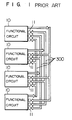
- a so-called analogue computer includes a plurality of functional blocks such as adders, integrators and others, wherein each of the functional blocks receives signals outputted from the other functional block or blocks directly or by way of a scaler circuit having a multiplication function, a sign inverter and others.
- the functional block then performs arithmetic operations such as addition, integration and other on the signal as received to thereby determine its own output value which is then transmitted to the other functional block or blocks.
- arithmetic operations such as addition, integration and other on the signal as received to thereby determine its own output value which is then transmitted to the other functional block or blocks.
- it is determined by operator in accordance with problems as imposed which of the functional block's output is to be inputted to which of the functional blocks and what a numerical value is to be set in the scaler circuit.
- a plurality of cell bodies and functional circuits 10 referred to as dendrites, wherein each of the functional circuits receives signals outputted from the other functional circuit through the medium of a scaler 11.
- Each of the functional blocks each composed of the functional circuit 10 and the scaler circuit 11 arithmetically determines a total sum of the values represented by the signals as its own internal value and outputs a signal corresponding to the internal value to the other functional blocks.
- Selection of the coefficients (hereinafter referred to as the weight values) for the individual scalers are automatically determined through a process usually referred to as the learning.
- An example of this type neural network is disclosed in a Japanese periodical "NIKKEI ELECTRONICS", No. 427 (August 10, 1987), pp. 115-124.
- NIKKEI MICRODEVICE An attempt for implementing the neural network in the form of a semiconductor integerated circuit is disclosed in a Japanese periodical "NIKKEI MICRODEVICE", July 1988, pp. 44-89.
- One of such semiconductor integrated circuits for the neural network is also discussed in "A CMOS ASSOCIATIVE MEMORY CHIP BASED ON NEURAL NETWORKS”: 1987 ISSCC DIGEST OF TECHNICAL PAPERS, pp. 304-305.
- NIKKEI MICRODEVICE July, 1988, pp. 72 to 78, there is proposed a neural network by using digital circuits.
- the digital circuits are easy to be integrated and can ensure a high accuracy for operations by virtue of high insusceptibility to noise and manufacturing tolerance.
- An implementation of a neural network on a digital multiprocessor system is disclosed in "THE FIFTEENTH ANNUAL INTERNATIONAL SYMPOSIUM ON COMPUTER ARCHITECTURE", May 30 to June 2, 1988, Honolulu, Hawaii, pages 3 to 11, from which the pre-characterising first part of claim 1 starts out.
- Each processor emulates a number of neurons by means of software. Connection between neurons of different processors is made by packet data transfer on a network interconnecting the processors. More details of data transmission over a network bus are disclosed in EP-A-200 365 which relates to a system for controlling communications on a network, interconnecting programmable controllers in an industrial plant. Time slots are assigned to active controllers so that they can transmit their data over the network bus to a specific other controller to achieve peer-to-peer communication.
- An information processing system may be a neural network implemented as an analogue computer or a large scale neural network implemented by using digital circuits for example.
- An implementation of the present invention is capable of structurizing a large scale neural network without lowering the yield rate regardless of increasing the number of neurons.
- Another implementation of the present invention is capable of implementing a high-speed large scale neural network while suppressing degradation in the operating speed due to increasing in the number of neurons.
- An implementation of the present invention is capable of realizing a large scale neural network by using a relatively small number of different photomasks.
- An implementation of the present invention is a neural network for an analogue computer for digital communication, in which the weight values as well as the output values of the neuron circuits can be expressed by a multiplicity of bits and which allows data processings of large scale without need for increasing the area for implementing the neural network.
- an implementation of the present invention allows a learning process to be executed normally even when fault should take place in a learning circuit system and which allows a neural network to be realized with an excellently high integration density.
- One implementation of the invention is an information processing system which includes a plurality of functional blocks (neurons) and a bus for transmitting in common the outputs of the individual functional blocks (neurons), wherein data transaction among the functional blocks (neurons) is performed through the data bus on a time-division basis.
- addresses are assigned to the individual blocks (neurons), respectively, so that only the functional block (neuron) having the own address designated by the address signal supplied through an address bus can output data signal onto the data bus, while the other functional blocks (neurons) receives the information on the data bus as the signal originating in the functional block whose address is designated at that time point.
- the addresses are sequentially changed.
- a semiconductor memory for storing the weight values only in a predetermined number sequentially in the order starting from the maximum absolute value of the weight.
- the bus for mutually connecting the functional blocks is implemented in a hierarchical structure.
- the hierarchical structurization of the buses is attended with a problem that occurrence of faults such as breakage, short-circuits and the like in the bus of higher hierarchical level exerts adverse influence over a wide range and lowers the yield rate.
- This problem can be solved by increasing the width of the wiring conductors for the bus of higher hierarchical level as well as the space between the bus conductors to thereby reduce the fault ratio.
- parts of the buses are shifted in position for connection to adjacent blocks.
- the integrated circuits of utterly the same configuration disposed in an array can be supplied with signals different from one to another integrated circuit.
- a WSI wafer scale integrated circuit
- a learning circuit is provided separately from and in common to the individual neurons (functional blocks), and realized in a structure in which fault can be removed.
- the inter-neuron data transmission is performed by using analogue signal, wherein determination of products and a sum thereof (multiplication and addition operation) is carried out through analogue calculation or alternatively the multiplication is carried out by an analogue calculation with the addition being performed by digital calculation.
- the neuron circuit can be realized with a smaller number of constituent elements. Because of the inter-neuron data transfer by the digital signal, there arises no problem that the signal undergoes attenuation due to the resistance of the wiring conductors, as in the case of the data transfer by the analogue signal, even when a great distance intervenes between the individual neurons (functional blocks) in a large scale neural network.
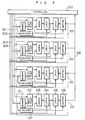
- Fig. 2 is a schematic block diagram showing a general arrangement of an information processing system according to an exemplary embodiment of the present invention.
- a reference numeral 10 denotes a functional unit
- a numeral 11 denotes a scaler circuit
- a numeral 12 denotes a time division control circuit
- a numeral 300 denotes a data input/output bus
- a numeral 302 denotes an address bus
- a numeral 303 denotes a clock bus
- a reference numeral 120 denotes a timing generation circuit.
- Fig. 3 is a block diagram showing in further detail the structure of one functional block (also referred to as a neuron) 100 which is constituted by the functional circuit 10, the scalar circuit 11 and the time division control circuit 12.
- the functional circuit 10 is composed of an adder 103, latch circuit 104 and 105 and a buffer circuit 106 having tri-state outputs.
- the scaler circuit 11 is constituted by a multiplier 102.
- the time-division control circuit 12 is composed of address decorders 107 and 107' and a memory circuit 101.
- the address decoder 107' serves to detect that the address signal sent via the address bus 302 has made a round, while the address decoder 107 serves to make decision as to whether or not the address signal is destined to the functional block under consideration. More specifically, assuming that the number of the functional block is represented by N, then the addresses "1", “2", “3", ..., “N”, by way of example, are assigned to blocks 100 each constituted by the functional circuit 10, the scaler 11 and the time division circuit 12, wherein the address signals are repeated in the sequence of "0", "1", "2", “3", ..., “N”, "0", "1", “2", “3” and so forth, wherein the address "0" is assigned to none of the functional blocks and made use of for detecting that the address signals enumerated above has made one round.
- the memory circuit 101 serves to store therein coefficients (weight values) for coupling between the functional block paired with the memory circuit 101 and other functional blocks and outputs the coupling coefficient (weight value) when the output of a functional block designated by the address signal at a given time point is inputted to the functional block paired with the memory circuit. At that time point, the output from the functional block designated by the address signal is present on the data bus 300. Accordingly, the multiplier 102 outputs a product of the signal from the abovementioned functional block and the coupling coefficient (weight value), whereon the product signal is applied to the adder 103.
- Fig. 4A and 4B show, by way of example only, circuit configurations of the address decoders, respectively. More specifically, the circuit shown in Fig. 4A is used as the address decoder 107' mentioned above, the output of which assumes a high level only when all the inputs are "0", i.e. when the address signal indicates the address "0", and otherwise assumes a low level. On the other hand, the circuit shown in Fig.
- the address decoder 107 is employed as the address decoder 107, the output of which assumes the high level only when the address signal indicates its own address (i.e. the address allocated to that decoder 107) and otherwise assumes the low level.
- the address of concern can be established in an arbitrary manner by placing an inverted bit(s) at a given bit position(s) of the address signal.
- the number (N - 1) of the scaler circuits which have heretofore been required to be incorporated in each of the functional blocks in a number corresponding to that of the other functional blocks in the prior art system can be reduced to one for each of the functional blocks.
- the number of the address which have heretofore been required to be incorporated in each of the functional blocks in a number (N - 1) corresponding to that of the other functional blocks can be decreased down to one for each of the functional blocks.
- a numerical value expressed by a number of pulses can be expressed in the form of a pulse code. This in turn means that increasing in the processing time which has heretofore given rise to a problem in the time division processing is canceled out to great advantage.
- the output of the functional block assigned with the address "1" is defined to be X while that of the functional block having the address "2" is defined to be Y.
- the inputs to the functional blocks or the integrators are represented by the differentials of the outputs, respectively. Accordingly, the following expressions apply valid: d dt X, d dt Y Accordingly, arrangement may be made such that the signal applied to the functional circuit 10 through the scaler circuit 11 can be given by the right-hand side of the expression (1) or (2) mentioned above.
- the memory circuit 101 assigned with the address "1" is placed with "0" at the zero-th address, ⁇ a at the first address and ⁇ b at the second address, while the memory circuit assigned with the address "2" is placed with "0" at the zero-th address, ⁇ c at the first address and ⁇ d at the second address.
- the latch circuits 104 are placed with the initial values of X and Y, respectively. Now, the preparation for the integration has been completed.
- Operation for the calculation is effectuated by generating by means of the timing generation circuit 102 the address signals repeating "0", “1", “2”, “0”, “1”, “2”, “0”, “1” and so forth every frame onto the address bus 302 and the clock signal containing one pulse for each frame onto the clock bus 303.
- the address signal is "0" in the first frame. Accordingly, the outputs of both the memory circuits 101 one of which is shown in Fig. 3 are “0". Consequently, the outputs of both the multipliers 102 are also "0".
- the output of the adder 103 is equal to the output of the associated latch circuit 104, i.e. the initial value of X or Y.
- the latch circuit 105 fetches the output of the latch circuit 104, i.e. the initial value of X or Y in response to the clock signal contained in the instant frame. Subsequently, in the second frame, the address signal becomes "1", resulting in that the buffer circuit 106 of the functional block assigned with the block address of "1" is activated, while the content of the latch circuit 105 of the block address "1", i.e. the initial value of X is outputted onto the data bus.
- the memory circuit 101 of the block address "1" outputs " ⁇ a”
- the memory circuit 101 of the block address "2" outputs " ⁇ c”. Consequently, the outputs of the multipliers 102 are “ ⁇ aX” and “ ⁇ cX”, respectively. Accordingly, the outputs of the adders 103 are "X + ⁇ aX” and “Y + ⁇ cX”, respectively, which are then fetched by the latch circuits 104, respectively, in response to the clock signal within the instant frame. Since no clock signal is applied to the latch circuits 105, they continue to remain in the state where the original values of X and Y are held as they are.
- the address signal becomes "2"
- the initial value of Y is outputted onto the data bus, as the result of which the memory circuits 101 output " ⁇ b” and " ⁇ d", respectively.
- the adder 301 adds " ⁇ bY” or “ ⁇ dY” to the output of the associated latch circuit 104 to thereby output "X + ⁇ (aX + bY)" or "Y + ⁇ (cX + dY)".
- the above value represents the value of X or Y after lapse of the minute time ⁇ from the initial state.
- the functional block 10 can be operated as the adder.
- the integrator or alternatively as the adder by controlling correspondingly the generation of the reset signal mentioned above.
- the multiplier 102 and the adder 103 can be so operated as to be capable of handling the negative numbers in terms of corresponding complementary numbers.
- the latch circuit 105 is not necessarily required when the time pace ⁇ for the integration is selected to be sufficiently small.
- the circuits themselves of the analogue computer described above are realized by the digital circuits. Accordingly, although the instability such as drift or phenomena inherent to the analogue circuits can be avoided, consideration must be paid to the instability ascribable to the principle of the analogue computer such as the positive feedback and others.
- the circuits themselves are realized by analogue circuits. For this reason, the cost of the analogue computer increases abruptly when the accuracy on the third or higher order of magnitude is to be realized. In reality, it has been unrealistic or impractical to realize the accuracy on the third or higher order of magnitude.
- the accuracy can readily be enhanced merely by increasing the number of the bits, since the circuits themselves are digital circuits.
- the wiring of the functional blocks to one another can be realized merely by writing the wiring information in the memory circuits 101 which can be easily integrated.
- the wiring information can be saved in a storage medium such as a magnetic disc or the like.
- the wiring information can also be automatically generated to be automatically written in the memories or storage equipment.
- the functional block 100 shown in Fig. 3 corresponds to a single unit referred to as a neuron, so to say, while the scaler 11 corresponds to a synapse for receiving signals from the other neurons with the combination of the adder 103 and the latch circuit 104 corresponding to a so-called dendron (of the cell body).
- Weighting of the individual synapses is realized by storing the weight coefficients in the memory circuits 101.
- the negative weight coefficient provides a suppressing effect, while the positive weight coefficient provides an exciting effect. As the absolute value of the coefficient increases, the weight becomes more significant.
- the numerical value represented by the output of the latch circuit 104 is utilized as the output value of the associated function block as it is (or by discarding the less significant bits).
- the circuit for performing the numerical transformation is provided between the latch circuits 104 and 105 or between the latch circuit 105 and the buffer circuit 106.
- the numerical translation can be realized by a control apparatus (not shown) for controlling the whole system.
- the circuit for the numerical transformation in accordance with the polygonal function given by the expression (4) can be implemented in such a circuit configuration as shown in Fig. 6A, by way of example.
- a reference numeral 610 denotes input terminal and 611 denotes output terminal.
- a multiplier 603, selectors 604 and 605 and an adder 603 are the signals representative of numerical values "a”, “-a”, “1/2a”, “1", “0” and "1/2", respectively.
- the comparator 601 controls the selector 604 so that the signal representative of "1” is outputted from the output terminal 611.
- the comparator 602 controls the selector 605 so that a signal representative of the numerical value "0" is outputted through the output terminal 611.
- the numerical transformation in accordance with the function given by the expression (4) can be realized by using the circuit shown in Fig. 6A.
- the numerical transformation in accordance with the sigmoid function given by the expression (3) or other complicated functions can easily be realized by using a memory circuit 603, as shown schematically in Fig. 6B.
- output values are previously calculated for the input values, respectively, and stored in the memory circuit 608 at addresses designated by the input signals, wherein the data stored in the memory circuit 608 are read out as the output values 611 to be utilized by addressing the memory with the input signals 610.
- the numerical transformation can be realized no matter how complex the functions to be resorted to are.
- a neural network implemented according to an embodiment of the present invention by reference to Fig. 7.
- the neuron is generally denoted by a reference numeral 100.
- Fig. 7 For simplification of the description, only four neurons connected to one another are shown in Fig. 7. As described hereinbefore in conjunction with Fig.
- each of the neurons includes a memory 101 for storing the weight value, a multiplier 102 for multiplying an input signal thereto with the weight value, an adder 103 and a latch circuit 104 for determining a total sum of the products produced by the multiplier 102, a latch circuit 105 for storing the abovementioned sum, a buffer circuit 106 having tri-state output, and a decoder 107 for deciding whether or not the associated neuron 100 is selected.
- Each of the neurons 100 is connected to a control apparatus 200 via a bus.
- the timing generator 120 shown in Fig. 2 and the function transformation circuit shown in Fig. 6A or 6B are incorporated in the control apparatus or controller 200.
- reference numerals 301, 302, 303 and 304 denote buses for sending the input signal, address signal, clock signal and the cycle signal to each of the neuron 100 from the controller 200.
- a numeral 305 denotes a bus for sending the output signal from each of the neurons 100 to the controller 200.
- the cycle signal 304 may be generated on the basis of the clock signal 303 and the address signal 302 within each functional block (neuron) 100, as in the case of the embodiments illustrated in Figs. 2 and 3.
- the latch circuit 104 is so implemented as to fetch the data in response to the edge of the clock signal applied through the clock bus 303.
- Each of the neurons 100 is assigned with an address inherent thereto (also referred to as the neuron address or block address).
- the decoder 107 Upon occurrence of coincidence between the neuron address and the address signal supplied from the control apparatus 200, the decoder 107 outputs a signal indicating the coincidence in the address.
- the controller 200 sends out the address signal which represents repeatedly a sequence of the addresses of the individual neurons, the clock signals for allowing the latch circuits 104 to fetch the data every time the relevant addresses are designated, and the cycle signal which causes the latch circuit 105 to fetch the data every time the sequence of the addresses has made a round, respectively.
- the address signal sent simultaneously to the individual neurons 100 from the control apparatus 200 via the address bus 302 are applied to the decoder circuits 107, whereon only the buffer circuit 106 of the neuron designated by the address signal outputs the signal onto the output bus 305.
- the buffer circuits 106 of the other neurons remain in the state of high resistance (impedence). In this manner, the content of the latch circuit 105 of the neuron 100 designated by the address signal is sent to the control apparatus 200.
- the control apparatus 200 sends out the signal of concern to each of the neurons 100 via the input bus 301 as it is or after transformation in accordance with the sigmoid function or an approximating polygon function.
- the weight value for the counterpart neuron designated by the address signal at that time point is read out from the memory 101, whereon the product of the weight value and the input signal supplied from the control apparatus 200 via the input bus 301 is determined by the multiplier 102.
- the sum signal thus produced is then applied to the latch circuit 104.
- the latter fetches the sum data in response to the application of the clock signal supplied via the clock bus 303.
- the total sum of the signals from all the neurons and the weight value is determined in the latch circuit 104.
- the cycle signal from the bus 304 the total sum is fetched by the latch circuit 105 and represents the updated output value of the associated neuron 100. In this way, the system shown in Fig. 7 operates as a neuron network.
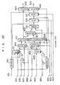
- Fig. 9 is a schematic circuit diagram showing a portion of an improved information processing system according to another embodiment in which buses are implemented in a hierarchical structure to evade the problem mentioned above. In this figure, one of functional block groups or neuron groups is shown. By interconnecting a large number of the circuits each of the configuration shown in Fig.
- FIG. 9 in such a manner as described hereinafter by reference to Figs. 10 to 13, there can be realized a large scale neural network.
- reference numerals 100 denote the neurons, respectively, and 301 to 305 denote the buses of first hierarchical level (the lowmost level). This portion may be implemented similarly to the neurons (functional blocks) and the buses 301 to 305 shown in Figs. 3 and 7.
- the bit number of the address bus 302 and the capacity of the memory 101 for storing the weight values have to be increased over those described hereinbefore in conjunction with Figs. 3 and 7 in order to be able to realize the large scale neural network.
- Fig. 9 reference numerals 100 denote the neurons, respectively, and 301 to 305 denote the buses of first hierarchical level (the lowmost level). This portion may be implemented similarly to the neurons (functional blocks) and the buses 301 to 305 shown in Figs. 3 and 7.
- the bit number of the address bus 302 and the capacity of the memory 101 for storing the weight values have to
- reference numerals 311, 312, 313, 314 and 315 denote buses of a second hierarchical level for transmitting the input signal, address signal, clock signal, cycle signal and the output signals, respectively.
- the buses 311 to 314 of those of the second hierarchical level send out the signals to the buses 301 to 304 of the first hierarchical level, respectively, through a buffer circuit 153, while the output bus 315 of the second hierarchical level receives the signal from the output bus 305 of the first hierarchical level by way of a tri-state buffer circuit 156.
- a decoder 157 serves for deciding as to whether or not there exists the neuron (functional block) 100 designated by the address signal in the neuron group (functional block group) 700 under consideration.
- the data on the output bus 305 of the first hierarchical level is sent out onto the output bus 315 of the second hierarchical level.
- the output of the tri-state buffer 156 is sent to the state of high resistance.
- Fig. 10 is a schematic circuit for illustrating a method of interconnecting the buses of the hierarchical structure.
- reference numeral 701 to 706 denote the functional block groups (neuron groups) each incorporating a plurality of the functional blocks (neurons) 100.
- the connection within each of the functional blocks as well as the interconnection thereof is made as shown in Figs. 2 and 7.
- reference numerals 300, 302 and 303 denote a data bus (including an input bus 301 and an output bus 305), an address bus and a clock bus, respectively.
- reference numerals 310, 312 and 313 denotes a high level data bus (input bus 311 and output bus 315), a high level address bus and a high level clock bus, respectively.
- the address signal and the clock are outputted onto the high level address bus 312 and the high level clock bus 313, respectively, from the timing generator 120 and supplied also to the address bus 302 and the clock bus 303 through drive circuit 722 and 723, respectively.
- Each of the drive circuits 722 and 723 corresponds to the buffer 158 shown in Fig. 9.
- different addresses are assigned to the individual function blocks (neurons), respectively, so that the functional block (neuron) can be definitely determined by the address allocated thereto.
- the data signal is coupled to the high level data bus 310 through the medium of bidirectional driver circuits 751 to 756 (each corresponding to the buffer 158 or 156 shown in Fig.
- the bidirectional drive circuit one of the circuits 751 to 756) constituting a pair with the functional block group or neuron group (one of the groups 701 to 706) which includes the functional block (neuron) 100 designated by the address signal transkits the signal on the low level data bus 300 onto the high level data bus 310, while the other bidirectional drive circuits transmit the signal from the high level data bus 310 onto the low level data bus 300.
- the output of the functional block (neuron) designated by the address signal is transmitted simultaneously to all the functional blocks (i.e. all the neurons).
- a functional block group corresponding to the whole circuit structure shown in Fig. 10 (except for the timing generator 120) as a structure of hierarchically high level together with higher level data bus, address bus and clock bus.
- the control of the bidirectional drive circuit in the manner described above can be realized, for example, by determining the address signal such that the more significant bits thereof designate the functional block group (neuron group) with the less significant bits designating the individual functional blocks (neurons), wherein only the more significant bits are applied to address decoder such as that shown in Fig. 4 to obtain the control signal.
- Fig. 11 shows a neuron network of an improved structure according to another embodiment of the invention in which the processing time is shortened in consideration of the facts mentioned above.
- reference numerals 701 to 706 denote, respectively, the functional block groups or neuron groups of the structure similar to those shown in Figs. 9 and 10.
- the address signal and the clock signals are supplied from the timing generator 120 to a high level address bus 312 and a high level clock bus 313, respectively, and hence to an address bus 302 and a clock bus 303 through driver circuits 722 and 723, respectively, as in the case of the systems shown in Figs. 9 and 10.
- Difference of the structure shown in Fig. 11 from those shown in Figs. 9 and 10 can be seen in the connection of the data bus 300.
- each of the data buses 300 is interconnected with only both the adjacent data buses through the bidirectional driver circuits 851 to 856, wherein the bidirectional driver circuit transmits the signal from the functional block group or neuron group including the functional block or neuron designated by the address signal only to the two adjacent functional block groups or neuron groups.
- the functional block or neuron 100 indicated by hatching in the functional block group or neuron group 702 of the neuron network shown in Fig. 11 is designated by the address signal.
- the bidirectional driver circuit 852 transmits the signal from the functional block group (neuron group) 702 to the functional block group (neuron group) 852, while the bidirectional driver circuit 853 transmits the signal from the functional block group (neuron group) 702 to the functional block group (neuron group) 703.
- the bidirectional driver circuits 851 and 854 transmit no signal in either direction.
- the control mentioned above can be achieved by constituting each of the driver circuits 851 to 856 by a pair of buffer circuits of tri-state outputs connected together on the input side and the output side.
- the output of the functional block or neuron designated by the address signal is transmitted to the individual functional blocks or neurons incorporated in the functional block groups (neuron groups) 701, 702 and 703 but not to those of the functional block groups (neuron groups) 704, 705 and 706.
- the output of that functional block or neuron can be transmitted to the individual functional blocks or neurons included in the functional block groups (neuron groups) 704, 705 and 706 by the same address signal as that mentioned above.
- the output of the functional block (neuron) in the functional block group (neuron group) 701 can be transmitted to the functional blocks (neurons) included in the functional block groups (neuron groups) 701, 702 and 706, respectively, while the output of the functional block (neuron) included in the functional block group (neuron group) 704 can be transmitted to the individual functional blocks (neurons) of the functional block groups (neuron groups) 703, 704 and 705, respectively.
- the upper limit value of the address signal is determined to be constantly thrice as large as the number of the functional blocks or neurons included in the single functional block group (neuron group) regardless of the total number of the functional blocks or neurons in the neural network.
- the time taken for the address signal to make a round can remain constant independent of the total number of the functionoanl blocks or neurons.
- the data is to be transmitted only to the adjacent functional block groups (neuron groups). It should however be understood that data transmission can be made to take place not only to the immediately adjacent functional block groups (neuron groups) but also to those groups next thereto and hence among five functional block groups in total by correspondingly modifying the method of controlling the bidirectional driver circuits 851 to 856.
- the upper limit value of the address signal is five times as large as the number of the functional blocks (neurons) included in the single functional block group (neuron group)
- the number of the functional blocks or neurons to which data can directly be transmitted from the single functional block or neuron can be increased by a factor of "5/3".
- this can be achieved by replacing each of the functional block groups (neuron groups) 701 to 706 by the whole system shown in Fig. 10 (exclusive of the timing generator 120) which is then regarded to be one functional block group (neuron group).
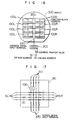
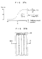
- FIG. 12 is a schematic diagram showing an improved structure of the neural network in which functional blocks (neurons) located two-dimensionally close to one another are interconnected. It should be noted in connection with Fig. 12 that only the frames of the functional block groups (neuron groups) are shown together with the data bus and the bidirectional driver circuits with details of the internal structure of the functional block group (neuron group), the address bus, the clock bus and the timing generator being omitted from illustration, being understood that they are similar to those described hereinbefore by reference to Figs.
- the control of the bidirectional driver circuits in the neuron network shown in Fig. 12 is performed in such a manner that when the address of a functional block or neuron included in a given one of the functional block groups (neuron groups) is designated, data is transmitted not only from the column including that given functional block group (neuron group) to the adjacent columns but also from the row including that given functional block group (neuron group) to the adjacent rows. More specifically, referring to Fig. 12 and assuming, by way of example, that one of the functional blocks or neurons included in the functional block group (neuron groups) 705 shown in Fig. 12 is designated, data is transmitted to the functional blocks (neurons) included in the functional block groups (neuron groups) 701 to 709, respectively. By virtue of this arrangement, it is possible to interconnect the functional blocks or neurons which are two-dimensionally located close to one another.
- the information processing system according to the invention is integrated in the form of a wafer scale integration semiconductor circuit (hereinafter also referred to as WSI in abbreviation).
- the wafer scale integration semiconductor circuit or WSI circuit it is contemplated to mean a semiconductor integration circuit integrated over a whole surface of the wafer size which can assure a higher degree of integration when compared with chip-like integration circuit obtained by cutting the wafer.
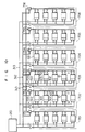
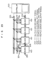
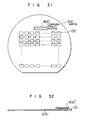
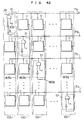
- Fig. 13 is a schematic view showing the information processing apparatus according to the invention which is realized in a single semiconductor substrate 500 in the form of the WSI (wafer scale integration circuit).
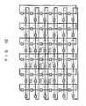
- reference numerals 700 denote the functional block groups or neuron groups described hereinbefore by reference to Figs. 9 to 12, wherein sixty functional block groups or neuron groups are shown in Fig. 13. It is assumed, by way of example, that each of the neuron groups (functional block groups) includes nine neurons (functional blocks) and thus 540 of neurons (functional blocks) in total are integrated in a single wafer.
- reference numerals 311 to 315 denote buses formed horizontally and having the second hierarchical level.
- a plurality of the buses are provided over the whole surface of the substrate.
- Reference numerals 321 to 325 denote buses of a third hierarchical level formed in the vertical direction. It will be noted that only one set of the vertical buses is provided at a center region of the substrate.
- the neuron groups (functional blocks) 700 are interconnected by the buses 311 to 315 of the second hierarchical level in a number ranging from two to four, wherein the buses 311 to 315 of the second hierarchical level are connected to buses 321 to 325 of a third hierarchical level by way of a buffer part 350.
- the buffer part 350 has a structure similar to the connection between the buses 301 to 305 of the first hierarchical level and the buses 311 to 315 of the second hierarchical level and includes the input buffer, the decoder and the output buffer, as in the case of the structures shown in Figs. 9 to 12.
- the control apparatus 200 which includes the timing generator 120 and the function transformation circuit shown in Fig. 6A or 6B. With this arrangement, it is possible to realize a neural network in which all the neurons (functional blocks) are interconnected while suppressing the maximum bus length to the diameter of substrate at the most.
- a power supply bus (not shown) can be so formed as to run in parallel with the buses 311 to 315 of the second hierarchical level so that the power can be supplied form power source parts 450 provided at both ends, thereby a large number of power source points can be assured.
- the wiring conductors to be used for the power supply bus (not shown), the buses 311 to 315 of the second hierarchical level, the buses 321 to 325 of the third hierarchical level should be greater in width than the wiring conductors 301 to 305 used internally of the neuron groups (functional block groups) 700 and the buffer 350 should be wired with a greater space. This is because care must be taken so that these buses 311 to 315 and 321 to 325 of great lengths should not present high wiring resistance and that the fault ratio should be lowered since otherwise occurrence of faults such a breakage, short-circuit and others in the buses of high hierarchical level will make inoperative many neurons (functioanl blocks) connected to these buses. For the failure which exerts influence to only a small number of the neurons (functioanl blocks), it is possible to exclude the neurons susceptible to the influenced of failure by setting the weight values thereof to zero on the side of the normal neurons (functional blocks).
- a buffer circuit (not shown) on the wafer 500 at the position of the control apparatus 200 in place thereof, wherein the buffer is connected to the control apparatus 200 provided externally of the wafer.
- the control apparatus 200 When a fault should occur in the control apparatus 200, the whole system is rendered inoperative. Accordingly, by providing the control apparatus 200 externally of the wafer 500 as described above, the control apparatus suffering a fault can easily be replaced or repaired. Besides, the fault ratio can be decreased by multiplexing the buffer circuit for the external connection or for connection of the control apparatus.
- the buffer circuit may be provided at a center portion where the yield is expected to be high.
- a plurality of substrates 500 may be provided and connected to buses of the fourth hierarchical level by way of the buffer circuit mentioned above to thereby interconnect the plurality of wafers 500 for the purpose of implementing a neural network of a larger scale, as will be described later on.
- the clock signal it is preferred to use a circuit assuring as high a transmission rate as possible so that the clock signal can travel from the bus 323 of the third hierarchical level to the bus 313 of the second hierarchical level and thence to the bus 303 of the first hierarchical level with a shortest possible propagation delay time. All the other signals are transmitted in synchronism with the clock signals of the relevant hierarchical levels.
- the address signal is supplied in such a manner in which the addresses "1" to "100” required for designating the individual neurons (functional blocks) and the addresses "101" to "105” required for the time division control are repeated with an interval corresponding to one clock being interposed upon return of the maximum address value "105" to the minimum address value "1".
- the addresses are shifted by one clock upon propagation from the second hierarchical level to the first hierarchical level. Since the individual neurons (individual functional blocks) are connected with the address bus 302 of the first hierarchical level (refer to Figs. 3, 7 and 9), the output value of the neuron (functional block) 100 designated by the address on the bus 302 is outputted onto the output bus 305 of the first hierarchical level. At this time, the abovementioned output signal is sent to the output bus 315 of the second hierarchical level and thence to the output bus 325 of the third hierarchical level while being shifted one by one clock in synchronism with the clock signal. The output signal is applied to the input bus 321 via the control circuit 200.
- the signal when synchronization with the clock signal is realized within the control circuit 200, the signal is shifted by one clock. The signal is then sent to the input bus 311 of the second hierarchical level and thence to the input bus 301 of the first hierarchical level while being shifted again one by one clock.
- the signal from the neuron (functional block) 100 designated by that address signal can reach all the neurons (functional blocks).
- the cumulative addition is performed for the signal by regarding that the signal originates in the neuron (functional block) of the address which is smaller by five than the numerical value indicated by the address signal.
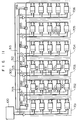
- Fig. 15 is a schematic circuit diagram showing a structure of the neural network which can dispose of successfully the problems mentioned above.
- Fig. 15 shows a right half of one row of the neuron groups (functional block groups) shown in Fig. 13.
- reference numeral 700 denotes generally the neuron groups (functional block groups), respectively.
- a numeral 100 denotes a neuron or a functional block
- numerals 311 to 315 denote buses of the second hierarchical level
- numeral 156 denotes a tri-state buffer
- a numeral 158 denotes a buffer circuit.
- a numeral 350 denotes a part for interconnecting the buses 321 to 325 of the third hierarchical level and the buses 311 to 315 of the second hierarchical level
- numeral 166 denotes a tri-state buffer
- 168 denotes a buffer circuit.
- the decoder 157 incorporated in each of the neuron groups (functional block groups) in the network shown in Fig. 9 is mounted in the connecting part 350 for interconnecting the buses of the third and second hierarchical levels.
- the output of the decoder 158 is sent to each of the neuron groups (functioanl block groups) 700 through a bus 316 of four bits.
- This bus 316 is so formed as to be shifted by one bit upon every passing through the neuron groups (functional block groups) 700, as can be seen in Fig. 15.
- the decoder 157 produces the output of high level only for the neuron groups (functional block groups) 700 that includes the neuron (functional block) 100 designated by the address signal. With such implementation, it is possible to select only the aimed one of the neuron groups (functional block groups) 700 notwithstanding that all the neuron groups (functional block groups) 700 are of the utterly same configuration.
- Each of the neurons 100 within each neuron group can make decision as to whether the neuron itself is selected or not with the aid of the two less significant bits of the address signal and the signal sent from the decoder 157.
- connection part 350 for selecting only one aimed row.
- the result of decoding the more significant bits of the address signal is sent to each of the connection parts 350 by way of the bus 326 of nine bits. Since the bus 326 of nine bits is so formed as to be shifted one by one bit for every row, it is possible to select the only one aimed row regardless of the utterly same configuration of the connection parts 350.
- the number of the photo-masks required for forming the neuro-WSI shown in Fig. 13 can be decreased to five sets, i.e.
- Fig. 16 is a view showing an improved structure of the information processing apparatus integrated in the form of WSI according to yet another embodiment of the invention.
- the illustrated structure is never limited to any specific number of the functional blocks or neurons. In practical applications, five hundreds or more functional block (neurons) can be integrated on a single wafer 500.
- 100R and 100L denote the functional blocks (neurons), and numerals entered in the blocks represent the addresses of the individual functional blocks or neurons 100R and 100L.
- a reference numeral 350 denotes a buffer part having address translation means 90 (refer to Fig. 17) for translating the input address signal to a signal differing therefrom for the output.
- a numeral 370 denotes an address input terminal to which the address signal is inputted.
- a numeral 200 denotes a control apparatus including an address pointer, and 38 designates an address pointer value outputted by the address pointer of the control apparatus 200.
- the addresses of the individual functional blocks (neurons) 100R and 100L at the time when the address pointer value 38 is "0000" are indicated by the numerals within the associated blocks, respectively.
- the number of the functional blocks (neurons) 100R and 100L is sixteen in total. Accordingly, for allocating the inherent or specific addresses to these neurons or functional blocks, four bits are sufficient for each functional block address. In the case of the example shown in Fig. 16, the two more significant bits of the four are used as the row address 3R with the two less significant bits being used as the column address 3L. Parenthetically, the bit number m for the actual address signal can be determined as follows: 2 m-1 ⁇ N ⁇ 2 m where N represents the number of the functional blocks or neurons.
- Fig. 17 shows the address translation means 90 incorporated in the buffer part 350.
- the buffer part 350 necessarily includes the buses for transmitting the clock signal and the data signal and the buffers, as described hereinbefore, they are omitted from the illustration in Fig. 16 for simplification with only the address signal translation means 90 being shown.
- This address translation means 90 corresponds to a part constituted by the address bus 326 and the decoder 157 shown in Fig. 15. In Fig.
- a reference numeral 370 denotes an input terminal for the address signal
- 6R denotes a right-hand output terminal for the address signal
- 6L denotes a left-hand output terminal for the address signal
- 6U denotes an upper output terminal for the address signal
- 108 denotes a one-incrementor
- 110 denotes an inverter circuit for outputting the input logic signal after having inverted it.
- the row address 3R constituted by the two more significant bit of the address signal inputted through the address signal input terminal 370 is added with "1" by the one-incrementor 108 to be then outputted to the upper output terminal 6U for the address signal.
- the one-incrementor 108 has two bit inputs and two bit outputs and realizes the translations or conversions of "00" to "01", “01” to “10", “10” to “11” and “11” to “00”, respectively.
- the other bits are outputted with the input values as they were.
- the address signal inputted through the address signal input terminal 370 is outputted intact from the right-hand output terminal 6R for the address signal 6R.
- Outputted from the left-hand output terminal 6L for the address signal is a signal which corresponds to the bit of the second least significance of the column address 3C of the address signal inputted through the address signal input terminal 370 and which has undergone the logical inversion in the inverter circuit 110.
- Figs. 18A and 18B show the functional blocks (neurons) 100L and 100R, respectively.
- a reference numeral 20 designates a functionoanl circuit which is designed in dependence on the contemplated or intended application of the WSI.
- the functional circuit 20 is so designed as to calculate neuron models and thus equivalent to the functional block or neuron 100 described in the foregoing.
- FIG. 18A and 18B arrangement concerning the address bus in the functional block 100 is shown with the other details being represented by the functional circuit 20.
- reference numerals 306 and 307 denote address signal input terminals, respectively, and 308 and 309 denote address signal output terminals, respectively.
- the functional block 100L receives the address signal inputted through the right-hand address signal input terminal 306 and outputs through the left-hand address signal output terminal 308 a signal which corresponds to the least significant bit of the column address 3C of the inputted address signal and which has been logically inverted by the inverter circuit 110.
- the functional circuit 20 receives the address signal via the address signal input terminal 306.
- the functional block 100R also receives the address signal inputted via the left-hand address signal input terminal 307 and outputs via the right-hand address signal output terminal 309 a signal corresponding to the least significant bit of the column address 3C of the input address signal which has undergone logical inversion through the inverter circuit 110.
- the functional circuit 20 is inputted with the address signal via the address signal input terminal 307.
- the four buffer parts 350 having the address signal translating function, the eight functional block 100R and the eight functional blocks 100L illustrated in Fig. 16 are connected in such a manner as mentioned below.
- the right-hand address signal output terminal 6R of the address signal translation block 90 incorporated in the buffer part 350 and the address signal input terminal 307 of the functional blocks 100R are connected to each other.
- the address signal output terminal 309 of this functional block 100R is connected to the address signal input terminal 307 of another functional block 100R.
- the left-hand address signal output terminal 6L of the address signal translation block 90 is connected to the address signal input terminal 306 of the functional block 100L.
- the address signal output terminal 308 of this functional block 100L is connected to the address signal input terminal 306 of another functional block 100L.
- the address signal input terminal 370 of the address signal translation block 90 is connected to the upper address signal output terminal 6U of the lower address signal translation block 90.
- Connected to the address signal input terminal 370 of the address signal translation block 90 located lowermost is the output of the address pointer provided in the control circuit 200.
- the functional block addresses of the individual functional blocks 100R and 100L connected in the manner described above are shown in Fig. 16 on the assumption that the address pointer value 38 outputted by the address pointer incorporated in the control circuit 200 is "0000".
- Fig. 19 shows the functional block addresses of the individual functional blocks 100R and 100L at the time point when the address pointer value 38 is "0111".
- the address pointer of the control apparatus 200 indicates various values
- the separate input addresses inputted to the individual functional blocks 100R and 100L vary correspondingly in dependence on the address pointer values. Accordingly, when the functional block to which a predetermined address (e.g. "0000") is inputted is to be the selected functional block, it is possible to select rather arbitrarily the functional block by varying correspondingly the address pointer value 38.
- the functional block 100R located on the bottom row at the second column as counted from the right corresponds to the selected functional block.
- the functional block 100L located on the topmost row at the first column as counted from the left is the selected functional block.
- Fig. 20 shows a functional block 100'L corresponding to the functional block 100L shown in Fig. 18B in the case where more than three bits are required for the column address.
- the column address 3C of the address signal inputted via an address signal input terminal 342 is added with "1" by means of a one-incrementor 141, wherein the address signal resulting from the above translation or conversion is outputted to an address signal output terminal 343.
- the functional block 100'L can be realized by using the one-incrementor 141 in place of the inverter circuit 110 shown in Fig. 18.
- the address signal translation or conversion is effectuated by addition of "1".
- the address signal translation may equally be effected by subtraction of "1".
- each of the functional blocks 100R and 100L is so arranged as to perform a predetermined translation on the input address to thereby output the address signal differing from the input address
- each of the functional block is inputted with the address signal inherent thereto so that any given one of the functional blocks can be selected by the address assigned thereto, whereby the address decoders of the individual functional blocks can be implemented in the utterly same structure. Accordingly, it is only necessary to prepare only three sheets of semiconductor reticle masks for the functional block 100L, the functional block 100R and the buffer part 350 including the address signal translation block 90, respectively. Thus, the cost involved in manufacturing the semiconductor reticle masks can remarkably be reduced.
- a wafer-scale semiconductor integrated circuit of a structure realized by using the functional blocks in a repetitive pattern in which a first address signal is inputted to a first functional block to undergo a predetermined translation, e.g. by addition or subtraction of "1" to or from at least one bit, and a second address signal differing from the first address signal is generated to be outputted to a second functional block.
- a predetermined translation e.g. by addition or subtraction of "1" to or from at least one bit
- the address signal generated externally of the wafer or by a circuit on the wafer is inputted to one part of the functional blocks, wherein each functional blocks translates the address signal inputted thereto to an address signal differing therefrom, which is the outputted to another functional block.
- the individual functional blocks are inputted with the address signals differing from one another, respectively.
- the address signal inputted to the one part of the functional blocks is modified or altered, the address signals inputted to the other functional blocks are also corresponding modified or altered.
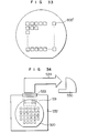
- Fig. 21 shows an improved structure of the weight value memory to be reduced.
- This memory circuit 101 is so structurized as to store only a predetermined number of the weight values orderly starting from the maximum absolute value in pairs with the counterparts' member's address, wherein the other weight values are regarded to be 0 (zero), to thereby reduce the storage capacity.
- reference numerals 111 and 112 denote memory cell arrays
- a numeral 113 denotes a pointer
- a numeral 114 denotes a comparator
- a reference numeral 115 denotes a selector.
- the array 111 is destined for storing the counterparts' or members' addresses
- the array 112 is for storing the weight values, wherein the members' addresses and the respective weight values are stored in pairs in the memory cell arrays on a row basis.
- the order of the storage rowwise is so selected that the addresses are arrayed in the ascending order.
- the address signals supplied from the control apparatus 200 to the individual neurons or functional blocks 100 through the bus 302 and others are sent in the ascending order.
- the pointer 113 is set to indicate initially the first row of the memory cell arrays 111, 112.
- the contents stored in the first row is read out, wherein the address information thereof is applied to one input terminal 122 of the comparator 114 while the weight value information is applied to one input terminal 124 of the selector 115.
- the address information applied to the comparator is of the smallest value of the address information stored in the memory address cell array 111.
- the address signal incoming from the control apparatus 200 through the buffer via the address bus 302 is applied to the other input terminal of the comparator 114. Since the address signals are supplied in the ascending order of the address value, the address signal continues to be of a small value till the first occurrence of coincidence with the signal 122 applied to the comparator 114, which value is thus absent in the memory cell array 111.
- the output 123 of the comparator 114 assumes a low level, as the result of which there makes appearance at the output terminal 126 of the selector 115 a numerical value of "0" which is applied to the other input terminal 125 of the selector 115.
- This output signal of the selector 115 represents the weight value for the counterpart member designated by the address signal 302 at that time point. In this case, the counterpart member's address is not stored in the memory cell array 111. In other words, the corresponding weight is of the small absolute value which is regarded to be 0 (zero), as mentioned above.
- the output 127 of the AND circuit 116 is also constantly at a low level with the pointer 113 remaining in the state to indicate the same row.
- the coincidence occurs between the address information applied to the terminal 122 of the comparator 114 and the address signal sent via the address bus 302, the output 123 of the comparator 114 assumes a high level, which results in that the weight value information applied to the terminal 124 of the selector 115 makes appearance at the output terminal 126 of that selector 115.
- This weight information represents the weight value for the counterpart designated by the address signal at that time point.
- the pointer 113 is changed over to indicate the next or second row.
- the selector 115 continues to output "0" until coincidence occurs between the address information stored at the second row in the memory cell array 111 and the address signal supplied via the bus 302, whereon the similar operation to that described above is repeated.
- the cycle signal is supplied via the bus 304, the pointer 113 regains the position to indicate first row again.
- the circuit shown in Fig. 21 operates to read out accurately the weights of the large absolute values which are stored in the memory cell array 112 while regarding the values of the other weights to be "0". Since the memory shown in Fig. 21 is necessarily read out in the ascending order, decision can instantaneously be made in response to the address signal as to the relevant information in present or not. Thus, the memory read-out operation can be performed without involving any appreciable increase in the access time.
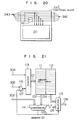
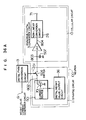
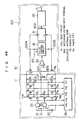
- Fig. 22 is a block diagram showing in further detail a structure of the neuron 100 (functional block) in accordance with a further embodiment of the invention.
- the memory 101 for storing the weight values, the multiplier 102, the adder 103, the latch circuits 104 and 105, the tri-state buffer 106, the decoder 107 and the buses 301 to 305 of the first hierarchical level operate in the manner described already by reference to Figs. 3 and 7.
- a shifter 807 and a selector 803 are provided for ensuring stabilized operation.
- a decoder 801, a selector 802, a tri-state buffer 804, a latch circuit 805, selectors 806 and 808 and buses 831 to 838 are provided to enable the neural network to make a self-learning.
- the shifter circuit 807 is so configured that the output value of the latch circuit 104 is shifted by a factor of 1/2 or 1/4 or 1/8 or so.
- the selector 803 is so implemented as to transmit ordinarily the output of the multiplier 102 to the adder 103 and to transmit the output of the shifter circuit 807 to the adder 103 in response to the application of the cycle signal (bus 304). Further, such arrangement is adopted that when the selector 803 transmits the output of the shifter circuit 807, the adder 103 performs subtracting operation.
- the selector 808 applies the output of the latch circuit 104 to the adder 103 except for the period of the self-learning mode.
- the adder 103 cooperates with the latch circuit 104 to perform ordinarily the cumulative addition described hereinbefore.
- the output of the latch circuit 104 is fetched by the latch circuit and multiplied with 1/2 or 3/4 or 7/8 or so to be subsequently applied to the input of the latch circuit 104 and fetched by the latch circuit 104 in synchronism with the clock signal (supplied via the bus 303), whereupon a new cumulative addition is started.
- a weight mean of the value calculated in the preceding cycle and the value to be calculated in the instant cycle is arithmetically determined. Although a time is taken until convergence of the result, oscillation is difficult to take place.
- the self-learning operation is carried out in a manner described below on the assumption that algorithm for the self-learning is based on a back propagation (the mathematical foundation of which is described in detail, for example, in a Japanese periodical "Nikkei Electronics", published August 10, 1987, pp. 115 et seq.).
- the cumulative adding operation is repeated to determine the output values of the neurons and store them in the respective latch circuits 105.
- the addresses of the neurons belonging to the output layer are sent out sequentially from the control apparatus 200 via the address bus 302 to read the contents of the latch circuits 105 into the control apparatus for determining the difference from an expected output value (the value of this difference is hereinafter referred to as the ⁇ -value), the difference value or ⁇ -value is written in the latch circuit 805 of the relevant neuron via the bus 823.
- the signal on the address bus 302 is fixed to the address of the neuron for which the ⁇ -value is to be determined, whereon the ⁇ -value of concern is determined through cumulative addition of the products of the weight values of the individual neurons for the neuron of concern and the ⁇ -value of the former.
- the weight value is read out from the memory 101 incorporated in each neuron with the ⁇ -value being read out from the latch circuit 805, respectively, whereon both values are applied to the multiplier 102 of each neuron via the selectors 802 and 806, respectively.
- the products are first determined.
- the addresses of the individual neurons are sent out from the control apparatus 200 via the bus 831, and the products mentioned above are read into the control apparatus 200 via the bus 832 to be cumulatively added for determining the ⁇ -value which is then written in the latch circuit 805 of the neuron of concern.
- the product of the ⁇ -value stored in the latch circuit 805 and an appropriate coefficient supplied via the bus 837 is determined by means of the multiplier 102 to be subsequently applied to one input terminal of the adder 103.
- the result obtained through addition of the weight value stored in the memory 101 and the value applied to the one input of the adder 103 is set as the updated or new weight value.
- Fig. 23 shows in a schematic circuit diagram an improve structure of the neural network which can enhance the yield of WSI according to a further embodiment of the present invention.
- reference numeral 203 denotes multiplex clock signal lines
- 351 denotes multiplex data buses
- 100 denotes neurons (functional blocks), respectively
- 203 denotes multiplex address signal input terminals
- 204 denotes multiplex address signal output terminals.
- the multiplex clock signal lines 355 are realized by multiplexing the clock signal line 303 in the embodiment described previously.
- the multiplex data buses 351 are realized by multiplexing the data bus 300 of the previously described embodiment.
- the address buses the decentralized or distributed control address system described hereinbefore by reference to Figs. 15 to 20 is adopted.
- the multiplex address buses are realized by mutliplexing the address signal line interconnecting the individual neurons (functional blocks).
- Numeral 201 denotes multiplex-data bus connection terminals and 202 denote multiplex clock signal input terminals.
- the multiplex address signal input terminals 204 of a given one of the neurons are connected to the multiplex address signal input terminals 203 of the adjacent neuron (functional block) 100.
- the multiplex address signal input terminals 203 of the neuron (functional block) 100 located at the input end of the network are connected to the address pointer incorporated in the control apparatus 200. Of course, the address pointer can be provided internally of the wafer.
- the multiplex data bus connection terminals 201 of each neuron (functional block) 100 are connected to the multiplex data buses 351.
- the multiplex clock signal input terminals 202 of each neuron (functional block) 100 are connected to the multiplex clock signal lines 355.
- the buffer part 350 including the address signal translation block is provided at the center of the neurons (functional blocks) 100, as described hereinbefore in conjunction with Figs. 13 and 16.
- the structure illustrated in Fig. 23 is only for the purpose of facilitating the description.
- Fig. 24A is a schematic circuit diagram showing an exemplary structure of the neuron (functional block) 100 suited for the multiplex bus structure according to a further embodiment of the invention.
- a reference numeral 211 denotes a majority circuit
- numeral 231 denotes a data input terminal
- numeral 232 denotes a data output terminal
- numeral 233 denotes a clock signal input terminal
- numeral 234 denotes address decoders, respectively
- numeral 212 denotes tri-state output buffers, respectively.
- Each of the tri-state output buffers has a signal input terminal for input signal, a signal output terminal for outputting an output signal and a control signal input terminal to which a control signal is applied, wherein the tri-state output buffer outputs the input signal to the output signal terminal or presents a high impedance state at the output terminal in dependence on the control signal.
- numeral 221 denotes address decoder input terminals
- 222 denotes an address decoder output terminal.
- a neuron model calculation unit 220 undergo logically majority decision on a bit-by-bit basis in the associated majority circuits 211, respectively, the results of which majority decision are supplied to a data input terminal 231, a clock signal input terminal 233 and to an address signal input terminal 234, respectively, of a neuron model calculation unit 220.
- the individual neurons 100 shown in Fig. 23 are selected one by one in correspondence with the address pointer values 38, respectively, as indicated by the address pointer to send out the output value onto the multiplex data buses 351.
- the signals of the multiplex data buses 351 are subjected to the majority logic on the bit basis by the majority circuit 211 shown in Fig. 24, the result of the majority logic being outputted to the neuron model calculation unit 220.
- the majority logic operation is performed in response to each of the clock signals supplied in multiplex via the multiplex clock signal line 355 shown in Fig. 23, whereon the results are outputted to the neuron model calculation unit 220.
- the address translation is effectuated by the one-incrementor 108.
- the signals before undergoing the address translation is subjected to the majority logic operation in the majority circuit 211 on the bit basis, the results of which are outputted to the neuron model calculation unit 220.
- the output value of the neuron model calculation unit 220 produced at the the other hand, the output of the neuron model calculation unit 220 is produced at the data output terminal 232 and outputted to the multiplex data bus connection terminals 201 through three tri-state output buffers 212.
- three signals inputted through the multiplex address signal input terminals 203 are supplied to three one-incrementors 108, respectively, to undergo address translation, the results of which are outputted through the multiplex address signal output terminals 204.
- the address decoder 210 may be implemented in the form of a NOR circuit, as shown in Fig. 24B.
- the control signal input terminals of the three tri-state output buffers 212 are connected in such a manner as shown in Fig. 24A.
- the neuron model calculation unit 220 is implemented in the same structure as that of the functional block (neuron) 100 as described hereinbefore by reference to Figs. 3 and 7. More specifically, the neuron model calculation unit has a terminal 231 corresponding to the data output terminal 232 is decided to be outputted or not onto the multiplex data buses 351 by the three tri-state output buffers 212 controlled by the address decoder 210. In the case of the structure as illustrated, the output of this neuron 100 is sent out onto the multiplex data bus 351 to be sent to the other neuron 100, when the address signals inputted are all "0".
- the number of the functional blocks (neurons) to be designed can be decreased, which in turn means that the number of the design steps can be correspondingly decreased.
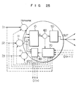
- Fig. 25 is a schematic diagram for illustrating the learning algorithm based on the back propagation method, in which one of the neurons (functional blocks) is shown.
- Reference symbols I1, I2 and I3 designate the output signals of the individual neurons (functional blocks) of the preceding layer or stage, and a reference symbol OUT designates the output signal of the neuron (functional block) of concern, which signal is inputted to the synapses 11 of the neurons (functional blocks) of the succeeding layer or stage.
- solid lines indicate signal flows in the ordinary operation with broken lines indicating signal flows in the back propagation learning mode.
- a reference numeral 10 represents a step for calculating the total sum of the input values multiplied with the weight values W. This step 10 corresponds to the functional circuit shown in Fig. 3.
- the reference numeral 50 represents a step for outputting a value resulting from the conversion or translation of the input value in accordance with a function f . Parenthetically, as the function used in the step 50, there is known the sigmoid function and others.
- a reference numeral 60 designates a switch which serves to change over the ordinary operation mode and the learning mode to each other.
- a reference numeral 70 represents a step for calculating a change d(n) of the synapse weight value in the learning mode.
- the weight values W of the synapses can be altered or changed in dependence on d(n), whereby the whole network can be structurized as to realize the desired input/output correspondence.
- the pattern associative type network structure and the back propagation learning algorithm provide great advantage in that not only the simulation on the computer system but also implementation as a semiconductor integrated circuit can be much facilitated. More specifically, in Fig. 25, it is easily possible to realize the part 11 in the form of a mutliplier circuit with a memory circuit, the part 10 as an adder circuit, the part 50 as a memory circuit, the part 60 as a switch circuit, the part 70 in the form of a combination of a multiplier circuit, an adder circuit and a memory circuit, and the part 80 as a multiplier circuit.
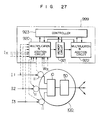
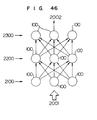
- Fig. 26 is a schematic diagram for illustrating the concept underlying the learning circuit according to the present invention.
- a reference numeral 99 denotes a learning circuit system which is provided separately from the individual neurons 100 and in common to them, and numerals 998 represent signal systems for the learning.
- a neural network shown as enclosed within a phantom-line block has the same structure as those described hereinbefore except that each of the neurons 100 has no learning circuit.
- the neural network enclosed by the broken line block executes normally the learning notwithstanding of occurrence of fault so long as the learning circuit system 999 is normal to thereby exclude the faulty neuron. Since the fault of the learning circuit according to the instant embodiment is previously remedied, no erroneously learned signal is transmitted to the neural network.
- the learning is executed, for example, in the manner mentioned below. Namely, the synapse weight values of the neurons of a layer Lm are fetched by the learning circuit system 999 and rewritten into the original synapses after alternation of the weight value. This processing is executed for the neurons of the layer Lm one by one, whereon the similar processing is executed for the neurons of a layer Ln.
- the learning circuit system 999 is constituted only by the circuits 11, 10, 60, 70 and 80 and by a control circuit for allocating these circuits in common to the individual neurons or functional blocks. Accordingly, the learning circuit system can be implemented with a high integration density.
- Fig. 27 is a diagram for illustrating an exemplary structure including the learning circuit system provided in common and a neuron 100 from which the learning circuit has been removed. Parenthetically, details of the functional blocks corresponding to the structure shown in this figure will be explained later on by reference to Figs. 28 and 29. Further, an exemplary embodiment of the fault remedy system for the learning circuit will be described hereinafter.
- reference numeral 99o denotes the learning circuit provided in common to the neurons (functional blocks), and 100 denotes a neuron from which the learning circuit has been removed.
- the synapses (combination of a multiplier circuit and a memory circuit 50) are equivalent to those shown in Fig. 25.
- a numeral 920 denotes a multiplication and addition circuit for multiplying the input signals I1 to In to the individual system synapses with the weight values W thereof and determining the total sum of the products resulting from the multiplication.
- This circuit 920 is equivalent to the circuit 11 and 10 described hereinbefore.
- a reference numeral 921 denotes a memory circuit for outputting a differential value of the function f described hereinbefore by reference to Fig. 25.
- a numeral 922 denotes a multiplication and addition circuit for determining D(n) and d(n), as described hereinbefore by reference to Fig. 25. Circuit 921 and 922 are same as those designated by 70 and 80, respectively, in Fig. 25.
- the circuits 920, 921 and 922 are used in common to the individual neurons (functional blocks).
- a numeral 923 denotes a control circuit for controlling sequential allocation of the learning circuit to the individual neurons in a consolidated manner.
- the circuits 920, 921 and 922 are each of such a small scale as can be included in a single neuron shown in Fig. 25.
- the learning circuit 999 also requires as small an area as on the order of 0.5 cm 2 even in case the control circuit 923 is included. Accordingly, the yield rate of the learning circuit 999 is on the order of 60%. Since no fault is present in the network whose yield rate is thus 100%, the yield of the semiconductor integrated circuit device as a whole is equal to the yield of 60% of the learning circuit 999 provided separately from and is common to the neuron.
- reference symbols Ix and Wx represent wiring lines coupled to the weight values and the output values of the other neurons, respectively.
- Fig. 28 is a circuit diagram for illustrating details of the circuits 11, 10 and 50 shown in Fig. 27.
- Fig. 28 from the input signals I1 to I3 to the synapses 11 and the weight values W stored in the associated weight value registers 1111, products given by I x W are calculated by the multipliers 1100, respectively.
- the results of the multiplication are successively selected by a selector circuit 1112 to be added sequentially by an adder 1113.
- the result of the addition is inputted to a table I/O (input/output) circuit 1114, wherein a function value f corresponding to the result of the addition is selected from a f-function table (memory) 1115 and sent out as the output of the so-called cell.
- I/O input/output
- Fig. 29 is a circuit diagram for illustrating details of the circuits 920 to 923 shown in Fig. 27. Coupled to selector circuits 1010 and 1011 are the output signal I1 to In of the individual neurons and the weight values W1 to Wn of the individual synapses, respectively. Select signals 2000 and 2001 are outputted from address generating circuits 1000 and 1001 incorporated in the control circuit 923, respectively. The output signal of the neuron and the weight value selected by the selector circuit 1010 and 1011 are held by register circuits 1007 and 1012, wherein the product thereof given by I x W is determined by a multiplier 1008. A numeral 1013 denotes a buffer circuit for writing in an reading out the synapse weight value.
- the results of the multiplications by the multiplier 1008 are successively added by an adder 1009.
- the result of this addition corresponds to s appearing in the expression (1).
- the result of addition s is inputted to a table I/O (input/output) circuit 1014, whereon a function f' corresponding to the addition result s is selected from a f'-function table 1015.
- a multiplier 1017 is destined to execute the multiplication given by the expression (6) mentioned hereinbefore.
- the result d(n) of this multiplication is inputted to an adder 1016 to be added with the weight value W not updated and held in the weight value register 1012.
- the result of this addition represents the updated synapse weight value, i.e.
- the updated value W is written into the individual synapse weight value registers (denoted by 111 in Fig. 28) incorporated in the network by way of the weight value register 1012, the read/write (R/W) buffer 1013 and the selector circuit 1011.
- a multiplier 1020 serves to determine the product of the value W held in the weight value register 1012 and d(n) in accordance with the expression (7) mentioned hereinbefore.
- the adder 1021 and the register 1022 cooperate to add sequentially the results of multiplication performed by the multiplier 1020 to thereby determine a total sum of D(n) and holds this determined value until the learning for the neurons belonging to the succeeding layer is executed, whereupon the value of D(n) is transferred to the register 1019.
- a reference numeral 923 denotes a control circuit for controlling the learning process (weight value updating process) described above. The control is performed in synchronism with the clock signal inputted through a terminal 1005.
- a numeral 1004 denotes a distributor circuit for supplying the clock signal to individual circuit blocks constituting the parts of the control circuit 923.
- a timing signal generating circuit 1003 generates a timing signal. In accordance with this timing signal, a series of the learning processes, i.e. data transfer to the register, successive or sequential additions and multiplications are executed.
- a reference numeral 1002 denotes an I/O interface circuit for connection with the external circuits.
- An external control signal and other inputted through an input/output pin 1006 is decoded by the I/O circuit 1002 which is turn sends control signals to a synapse address generating circuit 1000, a neuron output signal line address generating circuit 1001 and the timing signal generating circuit 1003.
- the select signals sent from the synapse address generating circuit 1000 and the neuron output signal line address generating circuit 1001 the selection of the values I and W described previously is executed.
- Fig. 30 is a diagram showing an exemplary structure for remedying fault of the learning circuit.
- reference numeral 999' denotes a learning circuit provided separately and in common such as, for example, the one shown in Fig. 9.
- the learning circuits 999' in quintuplet.
- a numeral 997 denotes a switch circuit for selecting one of the outputs d(n) of the quintuple learning circuits 999'.
- the probability of at least one of the quintuple learning circuits being faultless is 99%. It is possible to increase the yield by further increasing the number of the learning circuits manufactured in multiplex.
- the size of one learning circuit 999' is no larger than about 0.5 cm 2 . Accordingly, the area required by the five learning circuits as a whole amounts to no more than about 2.5 cm 2 and at the most 3 cm 2 inclusive of the switch circuit 997. The area is only about 5% of the device forming region of a 5-inch wafer. Fig.
- FIG. 31 is a schematic diagram showing a relation between the neural network and a learning circuit formed on a wafer according to an embodiment of the invention.
- reference numeral 800 denotes a learning circuit system constituted by the learning circuits 999' provided in multiplicity and the switching circuit 997 described above by reference to Fig. 30.
- Numeral 100 denotes the neuron incorporating no learning circuit, as shown in a lower half portion of Fig. 27.
- Fig. 32 is a schematic diagram for illustrating, by way of example, a further means for coping with the fault of the learning circuit.
- a reference numeral 500 denotes a wafer section in which a network of the neurons having no learning circuit is formed
- 800' denotes a semiconductor integrated circuit chip in section, which chip has a learning circuit 999' formed therein. It should be noted that this learning circuit is not provided in multiplicity.
- the chip 800' mounted on the wafer 500 is a faultless chip selected from a plurality of the chips 800' formed on a wafer, as shown in Fig. 33 and cut therefrom.
- the electrical connection of the wafer 500 and the chip 800' shown in Fig. 32 is realized by resorting to a flip-chip connecting method in which solder is employed as indicated by 30.
- the size of the chip 800' is 1 cm 2 .
- Fig. 34 is a schematic diagram showing still another exemplary embodiment for realizing a learning circuit 999 in a faultless structure. In the case of this embodiment, the circuit 999 is realized with the aid of a computer 550 which has already been ascertained to operate normally.
- a wafer 500 on which a neuron network is formed is mounted on a substrate 532.
- connection between the substrate 532 and the wafer 500 is realized by wire bonding as indicated by 530, while electrical connection between the substrate 532 and the computer 550 is established by using a connector 533 and a cable 534. Since the learning circuit 999 is implemented through cooperation of the computer 550 and a program running thereon according to the instant embodiment, the learning circuit system can positively finished faultless. In the case of the instant embodiment, not only the signal for learning but also the input/output signals are transmitted from the computer 550 through the media 531, 532, 533 and 534.
- Fig. 35 is a schematic diagram showing yet another embodiment of the invention in which a plurality of the abovementioned wafers are stacked in the vertical direction.
- numeral 500 denotes wafers each of which is packaged with an inventive learning circuit system 800 provided separately from and in common to the neurons. It should be noted that ten or more sheets of wafers 500 are stacked vertically. According to the instant embodiment, the wafers can be packaged very closely to one another, whereby a large scale neuron network circuits can be packaged at an extremely high density.
- the learning circuit 800 is formed in each of the wafer, the former can be provided in common to plural wafers groupwise.
- the learning circuit 800 can also be realized by packaging the learning circuit chip 800' shown in Fig. 32 by the hybrid method. Additionally, the learning circuit system may be connected to the computer 550 shown in Fig. 34 by the connector 533 mounted on the substrate 532 for thereby effectuating the learning control with the aid of the computer 550.
- a means for electrically interconnecting the wafers stacked in the vertical direction there can be mentioned, for example, a method disclosed in JP-A-56-2662.
- the information processing systems are wholly implemented by using the digital circuits. It is however noted that when only the multiplication and addition calculation or multiplication is performed by using an analogue circuit, the number of the elements which constitute one neuron can be decreased, whereby a large scale neural network can be realized.
- a large scale neural network is to be manufactured in which the weight values and the output values of the neurons can be expressed by a multiplicity of bits, an enormous number of neuron circuits naturally involve an increased area for the packaging, even when the number of the elements constituting the single neuron circuit is decreased. Consequently, when the neural network is to be implemented, for example, in the WSI (wafer scale integration), the inter-neuron distance is increased. However, by performing digitally the inter-neuron data transfer, the data transfer over a great distance can be realized when compared with the case in which analogue signals are used for the communication.
- a neuron constituted by a cellular model and a synapse model receives as inputs thereto the outputs of the others and assigns the weights to the latter, whereon the first mentioned neuron performs calculation mentioned below to produce an output value x i .
- each neuron Representing the outputs of N neurons of the identification numbers "0" to "N - 1" by x 0 , x 1 , ..., x j , ..., x N-1 , each neuron performs the calculation given by where a function f represents the sigmoid function given by where represents a threshold value and T represents a constant which is in general equal to 1 (one).
- the inter-neuron data transmission is performed by using digital signal, wherein the multiplication and addition calculation within each neuron is performed by resorting to analogue technique, the result of the analogue calculation being then converted to a digital signal.
- the output of the analogue neuron circuit of digital interface is many-valued, the input/output is performed in terms of the digital signal more insusceptibly to noise as compared with the case of the analogue signal.
- the multiplication and addition calculation is performed by using the analogue technique, the calculation can be realized with a smaller number of neuron constituting elements when compared with the case in which the digital signals are processed.
- Fig. 36A is a schematic diagram showing an exemplary embodiment of the neuron in which the inter-neuron data transmission is performed by making use of the digital signal while the intra-neuron multiplication and addition calculation is performed by the using analogue signals.
- the single neuron 100 is constituted by one cell-body or cellular circuit (functional circuit) 10 and one synapse circuit (scalar circuit) 11.
- the synapse circuit may be provided in any given number not smaller than one, inclusive.
- all the outputs of the synapse circuit 11 are connected to an input node 803 of the cell-body or cellular circuit (functional circuit) 10.
- the output terminal 71 of the cellular circuit (functional circuit) 10 also constitutes the output of the neuron 100.
- each of the other individual neurons 100 is coupled to an input terminal 61 of a digital PWM (pulse width modulation) conversion circuit 13 to be thereby converted to a pulse signal having a pulse width or duration proportional to the input value and outputted to an input node of the synapse circuit 11.
- the synapse circuit 11 weights the outputs from the individual neurons 100.
- a weighting current generator circuit 501 which is supplied at the input the weight values w ij for the neuron outputs from a digital weight value output circuit 36, which may be constituted by a memory or register or the like, wherein the weight values w ij may previously be written in the memory or register.
- the weighting current generating circuit 501 includes a current source 701 connected to an internal node 802 of the synapse circuit 11, which current source 701 generates a current of magnitude proportional to the weight value.
- a switch 504 serves for changing over the internal node 802 and the input node of the cellular circuit (functional circuit) 10 between the conducting state and the non-conducting state. This switch 504 is controlled by the pulse control signal applied to the input node 51 from the digital PWM conversion circuit 13. More specifically, the switch 504 sets the internal node 802 and the cell input node 803 to the conducting state only for a time corresponding to the pulse width of the pulse signal inputted to the input node 51.
- the current flowing into the cell input node 803 at that time is determined by the weighting current generating circuit 501. Consequently, the amount of electric charge flowing to the cell input node 803 is in proportion to the product w ij , x j of the neuron output value x j and the weight value w ij therefore.
- a capacity 507 is connected to the cell input node 803, whereby the potential at the cell input node 803 undergoes a change in proportion to the product w ij , x j .
- the potential at the cell input node 803 undergoes a change which is given by Such potential change may be brought about simultaneously by a plurality of the synapse circuits 2 connected to the cell input node 803.
- the multiplication and addition operation may be performed by utilizing the single synapse circuit 11 on a time-division basis.
- the capacity 507 is not the parasitic capacity but designed as mentioned below.
- the capacity 507 is so selected as to satisfy the following condition.
- C Q MAX / ⁇ MAX
- the capacity 507 can be realized by corresponding wiring in the case of LSI or by making use of the gate capacity of an existing MOS FET or by providing additionally a MOS FET for setting the capacity 507.
- an analogue-to-digital conversion A/D conversion
- a non-linear transformation or conversion in accordance with the sigmoid function
- the result of which is outputted to the output terminal in the form of the digital value.
- the potential at the cell input node 803 is converted to a digital signal by an analogue-to-digital converter 3, the digital signal being then outputted onto an internal data line 804 and subsequently inputted to a non-linear conversion circuit 26 to undergo the transformation in accordance with the sigmoid function, the result being finally outputted to the output terminal 71.
- the multiplication and addition operation is realized by storage or withdrawal of electric change in or from the capacity 507, which operation can thus be realized with a low power consumption. Further, since the electric charge is stored in the static capacity, the addition operation can be performed either in parallel or on a time-division basis.
- the weighting is realized by resistors connected between the outputs of neuron circuits and the inputs of the succeeding neuron circuits, wherein the initial multiplication and addition operation by summing the currents flowing through the resistors.
- the power consumption all the synapse circuit will amount to as high as 100 W in case the number of the neuron circuits is 500 with each neuron circuit including 500 synapse circuits.
- the power consumption in all the synapse circuits is as low as 5 W, when the current set by one weighting current generating circuit is 50 ⁇ A on an average, the time taken for coupling the current to the capacity by way of the switch 504 is 20 ns on an average, the time taken for the calculation for one neuron circuit in accordance with the expression (8) is 200 ns, and the source voltage is 4 V. In other words, the power consumption can remarkably be reduced according to the teaching of the invention.
- a pulse signal having the pulse width proportional to the input value may be utilized to the substantially same effect.
- Fig. 36B is a circuit diagram showing a modification of the embodiment shown in Fig. 36A which is designed to be realized in CMOS LSI.
- the operation for raising the potential at a cell input node 803 is referred to as “exciting” operation or “excitation” while the operation for lowering the potential at the cell input node 803 is referred to as “suppressing” operation or “suppression”.
- the excitation and suppression are controlled in dependence on a sign bit ⁇ s of the weight value outputted from a digital weight value output circuit 36.
- Fig. 36B it is assumed that the exciting operation is effective when the coded weight value bit ⁇ s is at a potential VVS (low level or "0") and the suppressing operation becomes effective when the coded weight value bit is a potential VDD (high level or "1").
- Source electrodes of a plurality of (e.g. four) PMOS FETs denoted by P 1 to P 4 , respectively, are connected to a power source VDD, drain electrodes thereof are connected to an internal node 810, and gates electrodes thereof are connected to sign bits ⁇ 1 to ⁇ 4 , respectively.
- MOS FETs denoted by N 1 to N 4 respectively, which have respective source electrodes connected to a power source VSS, drain electrodes connected to an internal node 811 and gate electrodes connected to the sign bits ⁇ 1 to ⁇ 4 weight value output circuit 36.
- a PMOS FET denoted by P 0 which has a drain electrode connected to the cell input node 803, a source electrode connected to an internal node 810 and a gate electrode connected to an internal node 812.
- a NMOS FET designated by N 0 which has a drain electrode connected to the cell input node 803, a source electrode connected to the internal node 811 and a gate electrode connected to an internal node 813.
- the switch circuit 504 is so designed that when the coded weight value bit ⁇ s is at low level, the pulse signal inputted to the synapse input node 51 is converted to a pulse signal which turn on the PMOS FET P 0 the pulse signal being outputted to the internal node 812, while when the sign bit ⁇ s at high level, the abovementioned pulse signal is converted to the pulse signal which turns on the NMOS FET N 0 , the pulse signal being then outputted to the internal node 813.
- an inverter circuit 22 having the input applied with the sign bit ⁇ s of the weight value and outputs the logical inversion thereof, a two-input NAND circuit 24 for performing NAND operation on the outputs of the synapse circuit input node 51 and the output of the inverter circuit 22, the result of the NAND operation being outputted to the internal node 812 and a Two-input AND circuit 24 for performing AND operation on the outputs of the synapse circuit input node and the sign bit ⁇ s of the weight value, the result of which is outputted to the internal node 813.
- conductances of the NMOS FETs N 0 to N 4 are represented by G n0 to G n4 ,
- G n0 >> G n1 •(2 0 + 2 1 + 2 2 + 2 3 )
- the conductance between the cell circuit input node 803 and the VSS can be approximated by the following expression; ⁇ s •G n1 ( ⁇ 1 •2 0 + ⁇ 2 •2 1 + ⁇ 3 •2 2 + ⁇ 4 •2 3 )
- the weight value current generating circuit 501 serves as a current source capable of supplying the current of magnitude substantially in proportion to the weight value.
- the weight value is expressed in five bits inclusive of the sign bit in the case of the embodiment shown in Fig. 36B, it is of course possible to use other number of bits to this end.
- the synapse circuit 11 After having set the weight value current generating circuit 501, the synapse circuit 11 applies the pulse signal to the input node 51 of the synapse circuit.
- the sign bit ⁇ s of the weight value is at a low level
- the PMOS FET P 0 is set to the on or conducting state for a period corresponding to the pulse width of the pulse signal representing the sign bit
- the NMOS FET N 0 is set to the on or conducting state for a period corresponding to the abovementioned pulse width when the weight value sign bit ⁇ s is at high level, whereby the electric charge is injected into the cell input node 803.
- the up-down counter 81 is reset before operation of the synapse circuit 11. Further, the cell input node and the internal node 805 of the cell circuit 1 are precharged to the potential (VDD + VSS)/2 volts, respectively. Subsequently, the multiplication and addition operation described hereinbefore is performed, as the result of which the potential at the cell input node 803 undergoes a charge corresponding to the value resulting from the multiplication and addition operation. Upon completion of the arithmetic operation of the synapse circuit 11, the cell circuit 1 compares the potential V N at the cell input node 803 with the potential V R at the internal node 805 by using the comparator 20.
- the pulse control circuit 18 applies the clock signal to the clock signal input terminal 201 and responds to the control signal outputted from the comparator 20 by applying the clock signal pulse to the internal node 2002 so that the PMOS FET P 10 is turned on when V N > V R while when V N ⁇ V R , the clock signal pulse is so converted that the FET N 10 is turned on to be subsequently applied to the internal node 2003.
- a PMOS FET P 10 having a drain electrode connected to the internal node 805, a source electrode connected to the VDD and a gate electrode connected to the internal node 2002 and a NMOS FET N 10 having a drain electrode connected to the internal node, 805, a source electrode connected to the VSS and a gate electrode connected to the internal node 2003, respectively.
- the pulse control circuit 18 stops transmission of the pulses.
- the pulses outputted from the pulse control circuit 18 is sent to the up-down counter 81 as well.
- the up-down counter 81 has the inputs connected to the internal node 2002 and the internal node 2003, respectively.
- the up-down counter counts up by +1, while the latter counts down by -1 upon application of the pulse to the internal node 2003 which causes the NMOS FET N 10 to be turned on.
- the content of the up-down counter 81 then represents the result of the multiplication/addition operation. This result is then outputted onto an internal data line 804.
- the cell input node 803 is precharged by a half as described hereinbefore to thereby perform the multiplication operation. In this case, resting of the up-down counter 81 is not effectuated and caused to operate as an accumulator.
- Fig. 37A illustrates graphically values taken by the sigmoid function taken along the ordinate with the input values being taken along the abscissa
- Fig. 37B shows a memory map.
- Fig. 37A values of the sigmoid function to be outputted for the addresses as inputted are written in the memory at the addresses corresponding to the values resulting from the multiplication and addition operation.
- the non-linear conversion circuit 26 internally contains the memory and receives at the input thereof the result of the multiplication and addition operation to thereby output the value written at the corresponding address to the output terminal 71.
- the output is a digital value.
- a plurality of the neuron circuit 100 described above is mutually connected to constitute a neural network, whereon the operation described in the foregoing is repeated.
- the arithmetic operation is executed until all the outputs of the neuron circuits 100 become stabilized (converge sufficiently).
- convergence to the optimum solution may be attained by performing a simulated annealing, which can be realized by changing the constant T (temperature) in the sigmoid function given by the expression (9).
- the non-linear translation or conversion circuit 26 is of such structure that the functions are written in the memory, wherein the memory content at the address corresponding to the input value is outputted, the simulated annealing can be performed in a facilitated manner by rewriting the content of the memory which is constituted by a RAM (random access memory).
- the weight value is handled in terms of the digital signal.
- the analogue signal is applied to the gate terminal of the MOS FET to control the conductance of the drain-source path of the MOS FET for thereby expressing the weight value and the input value in the form of the many-value.
- the result of the arithmetic operation is to be outputted in the form of many-value, it is difficult to control the abovementioned conductance of the MOS FET by the gate voltage because of the non-linear characteristics of the MOS FET.
- the multiplication/addition operation within the neuron circuit is performed by making use of the analogue process, while the input/output operation of the neuron circuit is performed digitally.
- the neuron circuit can be realized by a remarkably small number of constituent elements when compared with the neuron circuit implemented only by the digital circuitries.
- the input/output operation is performed by using the digital signal, there can be evaded such problems as noise margin and signal attenuation due to the wiring resistance to the analogue signal which may arise when the data transmission between the neuron circuits is performed by using the analogue signal, whereby design can be much simplified.
- Fig. 38 is a schematic circuit diagram showing a circuit configuration of the digital PWM converter 13.
- a reference numeral 2101 denotes an input terminal for a conversion start signal
- a numeral 2102 denotes a clock signal input terminal
- numerals 2103 to 2106 denote data input terminals, respectively
- a numeral 2110 denotes a 4-bit counter
- a numeral 2111 denotes a RS flip-flop
- a numeral 2112 denotes an AND circuit having four inputs
- a reference numeral 2110 denotes an inverter circuit.
- the counter 2110 is decremented one by one every time the pulse of the clock signal is inputted from the node.
- the output of the flip-flop 2111 becomes high.
- transmission of the clock signal to the node 2102 is started.
- the data already placed in the counter 2110 is decremented one by one every time the clock signal pulse is inputted.
- the output of the 4-input AND circuit 2112 becomes high, where the output of the RS flip-flop 2111 is reset to low level.
- the output of the RS flip-flop 2111 is maintained at high level for a period from the inputting of the conversion start signal to the inputting of a number of clock signal pulses having input values inputted to the input terminals 2103 to 2106.
- Fig. 39 is a schematic circuit diagram showing a Hop-field type neural network implemented by using N neuron circuits 100 according to another exemplary embodiment of the invention.
- each of the neuron circuit 100 is constituted by one synapse circuit 11 and one cell body circuit 10. Every two of the neuron circuits 100 are combined in a pair, wherein the cell input notes 803a and 803b of the paired neuron circuits 100 are connected to a half precharge circuit 41 which serves to precharge the cell input nodes 803a and 803b to a voltage level of (VDD + VSS)/2 volts. All of the output terminals of N neuron circuits 100 are connected to a time-division broadcast network 35.
- the time-division broadcast network 35 selects one of these output values to thereby output the values x 0 to x N-1 sequentially in this order to the digital PWM converter 13.
- the digital PWM converter 13 converts the output value of the each neuron circuit 100 to a pulse signal having a pulse width or pulse density proportional to the input value (i.e. output of the neuron circuit) to thereby send the pulse signal to the input terminals 51 of all the neuron circuits 100.
- N times the operation described above all the data as required by the neuron circuit 100 arrive at the individual neuron circuits 100. Since the multiplication and addition operation is performed on a time division basis in the case of the embodiment shown in Fig. 39, one neuron circuit 100 requires no more than one synapse circuit 11, whereby the amount of hardware can be reduced very significantly.
- Fig. 40A is a circuit diagram showing a configuration of the half precharge circuit 41
- Fig. 40B is a timing chart for illustrating operation of the half precharge circuit.
- reference numerals 150 and 151 denote clock signal input terminals
- 803a and 803b denote input terminals which are connected to the cell body input modes 803 two neuron circuits 100, respectively.
- Numerals 507a and 507b denote capacities connected to the cell body input nodes 803a and 803b, respectively.
- Reference numerals 71a and 71b denote the output terminals of the cell body circuit 10.
- the precharge operation is performed in such a manner in which the clock signal input terminal 150 is set to a high level with the clock signal input terminal 151 being applied with a low level, whereby the one cell body input node 803a is charged to a high level with the other cell body input node 803b being at the low level. Subsequently, when the low level is applied to the clock signal input terminal 150 with the high level being applied to the clock signal input terminal 151, the PMOS FET P 21 and NMOS FET N 21 are turned to the on or conducting state, whereby a short-circuit is formed between the two cell body input nodes 803a and 803b.
- the two cell body input nodes 803a and 803b can be respectively half-precharged to (VDD + VSS)/2 volts.
- Fig. 41 is a schematic circuit diagram showing a Hop-field type neural network which is realized by using N neuron circuits 100 each constituted by one cell body (cellular) circuit 10 and (N - 1) synapse circuit 11.
- N neuron circuits 100 each constituted by one cell body (cellular) circuit 10 and (N - 1) synapse circuit 11.
- the outputs of the all the synapse circuit 11 are coupled to one node of the cell body input nodes 803 (by wired-OR connection).
- Inputted to each synapse circuit 11 is the output from each neuron circuit 100, whereon the inputs is correspondingly weighted, and the amount of charge approximately proportional to the product is injected to each cell body input node 803 (803a - 803c, ..., 803z).
- the multiplication and addition operations are performed in parallel by the individual neuron circuits 100.
- the AD conversion and the non-linear transformation being followed by conversion to the pulse signal through the digital PWM conversion circuit 13, which pulse signal is then outputted to the input terminal 51 of the synapse circuit 11 of each neuron circuit 100.
- the cell body input node 803 (803a to 803c, ..., 803z) of each neuron circuit 100 is connected to the half-precharge circuit 41 such as the one shown in Fig. 39.
- Fig. 42 is a schematic circuit diagram showing a Hop-field type neural network similar to that shown in Fig. 41 but differs from the latter in that the output of each neuron circuit 100 is expressed by a single bit of "0" or "1". Because the output value of the neuron is expressed by the single bit, the cell body circuit 10 can be simplified as compared with that described above. More specifically, an inverter circuit 21 is connected to the cell body input node 803 (803a - 803c, ..., 803z), wherein two inputs of a 2-input AND circuit 24 are connected to the output terminal of the inverter circuit 21 and the clock signal input terminal 202, the output terminal of the AND circuit 24 being connected to the synapse input node 51 of each synapse circuit 11.
- Each neuron circuit 100 produces the output only when the clock signal input terminal 202 is high.
- a two-stage tree structure the four-input neuron circuits 100Q as the basic neuron circuits to thereby realize a 16-input neuron circuit 4T16 or a greater scale neuron circuit having a greater number of inputs by connecting the 16-input neuron circuits 4T16 in multiple stages, as shown in Fig. 43.
- reference numerals 1301 to 1316 denote input terminals of the synapse circuits.
- the structure shown in Fig. 43 may be implemented by using the basic neuron circuits each constituted by an eight-input neuron circuit or a two-input neuron circuit, as occasion requires. In this case, in each of the repeater cell body circuits 10 except for the cell body circuit 10 of the final output stage, a linear transformation (conversion) is performed rather than the non-linear transformation.
- Fig. 44 shows another embodiment of the present invention.
- the circuit is similar to the embodiment shown in Fig. 36B with regard to the synapse circuit 11 and differs slightly from the latter in respect to the structure of the cell body circuit.
- reference symbol P 5 designates a PMOS FET and N 5 designates a NMOS FET.
- the cell body input node 803 is precharged to (VDD + VSS)/2 (V) by the half-precharge circuit (not shown), whereby an up-down counter 81 is reset. Further, there is provided a cell body input node for applying the potential of (VDD + VSS)/2 (V) to the reference voltage input terminal 806.
- the PMOS FET P 5 has a drain electrode connected to the cell body input node 803, a source electrode coupled to VDD and a gate electrode connected to the internal node 2004.
- the NMOS FET N 5 has a drain electrode connected to the cell body input node 803, a source electrode connected to the VSS and a gate electrode connected to the internal node 2005.
- the clock signal is applied to the clock signal input terminal 201, and the output of the comparator 20 is used as a control signal. More specifically, when the result of the comparison performed by the comparator 20 is that V N ⁇ V R2 , the clock signal pulse is applied to the internal node 2004 which sets the PMOS FET P 5 to the on-state, while when V N > V R2 , the pulse is outputted to the internal node 2005 for turning on the NMOS FET N 5 . This operation is controlled by a pulse control circuit 18. After the pulse is outputted to the internal node 2004 or 2005 once or a plurality of times, V n becomes approximately equal to V R2 , whereby the output of the comparator 20 is ultimately inverted.
- the pulse control circuit 18 stops the transmission of the pulse signal.
- An up-down counter 81 is connected to the internal node 2004 and the internal node 2005 for counting "-1" in response to the application of the pulse to the internal node 2004 which turns on the PMOS FET P 5 , while counting "+1" in response to the application of the pulse to the internal node 2005 which turns on the NMOS FET N 5 .
- the value of the up-down counter 81 indicates the results of the multiplication and addition operation, which is then subjected to non-linear transformation by the non-linear transformation circuit, the result of which is outputted to the output terminal 11.
- the half-precharge of the cell body input node 803 can be effectuated to thereby realize the multiplication operation.
- the up-down counter 810 is not reset so that it operates as an accumulator.
- Fig. 45A shows an another cell body circuit lc for realizing the AD conversion circuit and the non-linear transformation circuit 26 according to a still further embodiment of the invention. Referring to Fig. 45, description will be made of operation which takes place in succession to the change in the potential at the cell body input node 803 as the result of multiplication/addition operation performed by the synapse circuit 11.
- a comparator 20 is provided for comparing the potential V N at the cell body input node 803 with a potential V R3 at a staircase wave output node 807 of a staircase wave generating circuit 25. Further provided is a counter 19 for counting the number of pulse outputted to a pulse output node 808 of the stircase wave generating circuit 25 under the control of the output signal of the comparator 20. The counter 19 is reset before performing the AD conversion and non-linear transformation. Subsequently, the potential V N is compared with V R3 by the comparator 20. The counter 19 continues to count the number of pulses outputted to the pulse output node 808 until the output of the comparator 20 is reversed.
- the value indicated by the counter 19 upon reversion of the output of the comparator 20 represents the result of the non-linear transformation or conversion.
- the staircase wave V R2 is outputted in the form of a inverse function f -1 (k) of the sigmoid function f for the number k of the pulses outputted to the pulse output node 808.
- Fig. 46 shows an example of the neural network of a hierarchical structure.
- the neuron circuit 100 is constituted by the synapse circuits 11 and the cell body circuit 10.
- an input pattern inputted as indicated by 2001 undergoes arithmetic operation through the neurons of an input layer 2100, an intermediate layer 2200 and an output layer 2300, the result of the operation being outputted through the neurons of the output layer 2300, as indicated by 2002.
Landscapes
- Engineering & Computer Science (AREA)
- Physics & Mathematics (AREA)
- Theoretical Computer Science (AREA)
- Health & Medical Sciences (AREA)
- Life Sciences & Earth Sciences (AREA)
- Biomedical Technology (AREA)
- Biophysics (AREA)
- General Health & Medical Sciences (AREA)
- General Physics & Mathematics (AREA)
- Evolutionary Computation (AREA)
- Computational Linguistics (AREA)
- Molecular Biology (AREA)
- Computing Systems (AREA)
- General Engineering & Computer Science (AREA)
- Data Mining & Analysis (AREA)
- Mathematical Physics (AREA)
- Software Systems (AREA)
- Artificial Intelligence (AREA)
- Neurology (AREA)
- Multi Processors (AREA)
- Complex Calculations (AREA)
- Small-Scale Networks (AREA)
Claims (11)
- Informationsverarbeitungssystem, aufweisendgekennzeichnet durch:mehrere Neuronen (100), die jeweils einen in Bezug zu den anderen Neuronen festgelegten Gewichtungskoeffizienten aufweisen und entsprechend der Gesamtsumme von Produkten des zugeordneten Gewichtungskoeffizienten und der Ausgabewerte anderer Neuronen einer Neuronengruppe einen Ausgabewert aussenden können,einen Adressbus (302) zur Übertragung eines die Neuronen sequentiell bezeichnenden Adressignals,einen Datenbus (300) zur Übertragung der von den Neuronen abgegebenen Ausgabewerte, undeine Einrichtung (107, 107', 105, 106), um den Neuronen jeweils nur dann zu gestatten, ihren Ausgabewert abzugeben, wenn sie von dem Adressignal bezeichnet werden.
- System nach Anspruch 1, das einen Zustand aufweist, in dem in einem Zyklus des Adressignals keines der Neuronen bezeichnet wird.
- System nach Anspruch 2, wobei die Neuronen jeweils eine Schaltung (106) zur Zwischenspeicherung ihres Ausgabewerts aufweisen.
- System nach einem der Ansprüche 1 bis 3, wobei die Neuronen in mehrere Gruppen (700, 701 bis 709) unterteilt sind und der Adressbus und der Datenbus jeweils in erste Busse (301 bis 305) zur jeweiligen Verbindung der Neuronen innerhalb einer Gruppe und einen zweiten Bus (311 bis 315) zur Verbindung der ersten Busse unterteilt sind.
- System nach Anspruch 4, wobei der zweite Bus mittels eines Leiters größerer Breite als ein Leiter für einen ersten Bus verdrahtet ist.
- System nach Anspruch 4, mit einem Taktbus (303) zur Lieferung eines Taktsignals an die Neuronen, so daß eine Übertragung zwischen einem ersten Bus und dem zweiten Bus synchron mit dem Taktsignal vorgenommen wird.
- System nach einem der Ansprüche 1 bis 6, wobei einige der Neuronen auf einem Halbleiterwafer (500) ausgebildet sind.
- System nach einem der Ansprüche 1 bis 7, wobei die Neuronen jeweils eine Adressübersetzungseinrichtung (90) zur Ausgabe eines von dem eingegebenen Adressignal verschiedenen Adressignals auf den Adressbus aufweisen, um ein eingegebenes Adressignal in für einzelne Verbindungsrichtungen des Neurons vorbestimmte einzelne Ausgangsadressignale zu übersetzen.
- System nach Anspruch 8, wobei die Adressübersetzungseinrichtung aus einer Einrichtung (108) zum Hinzuzählen oder Abziehen mindestens eines Bits zu oder von dem eingegebenen Adressignal aufweist.
- System nach Anspruch 8, wobei die Neuronen jeweils einen Adressdecoder (107) aufweisen, der darauf anspricht, daß das Adressignal ein vorbestimmtes Signal ist.
- System nach einem der Ansprüche 1 bis 10, wobei die Neuronen (100) jeweils eine Speichereinrichtung (101) zur Speicherung einer kleineren Anzahl an Gewichtungskoeffizienten als Neuronen in mit dem größten Absolutwert der Gewichtungskoeffizienten beginnender Reihenfolge aufweisen.
Applications Claiming Priority (10)
| Application Number | Priority Date | Filing Date | Title |
|---|---|---|---|
| JP299/89 | 1989-01-06 | ||
| JP64000299A JPH02181258A (ja) | 1989-01-06 | 1989-01-06 | ニューロネットワークを用いた半導体集積回路装置,その製造方法及びニューロネットワーク装置 |
| JP89300A JPH02181284A (ja) | 1988-02-18 | 1989-01-06 | ニューラルネットワーク |
| JP297/89 | 1989-01-06 | ||
| JP64000297A JP2765903B2 (ja) | 1989-01-06 | 1989-01-06 | 情報処理装置 |
| JP300/89 | 1989-01-06 | ||
| JP1056458A JP2804069B2 (ja) | 1989-03-10 | 1989-03-10 | 情報処理装置 |
| JP56458/89 | 1989-03-10 | ||
| JP26310389A JPH03125256A (ja) | 1989-10-11 | 1989-10-11 | ウェハスケール半導体集積回路 |
| JP263103/89 | 1989-10-11 |
Publications (3)
| Publication Number | Publication Date |
|---|---|
| EP0378115A2 EP0378115A2 (de) | 1990-07-18 |
| EP0378115A3 EP0378115A3 (de) | 1993-12-22 |
| EP0378115B1 true EP0378115B1 (de) | 1998-09-30 |
Family
ID=27517940
Family Applications (1)
| Application Number | Title | Priority Date | Filing Date |
|---|---|---|---|
| EP90100171A Expired - Lifetime EP0378115B1 (de) | 1989-01-06 | 1990-01-04 | Neuronaler Rechner |
Country Status (3)
| Country | Link |
|---|---|
| US (1) | US5165010A (de) |
| EP (1) | EP0378115B1 (de) |
| DE (1) | DE69032680T2 (de) |
Cited By (2)
| Publication number | Priority date | Publication date | Assignee | Title |
|---|---|---|---|---|
| US20160260008A1 (en) * | 2012-12-21 | 2016-09-08 | International Business Machines Corporation | Time-division multiplexed neurosynaptic module with implicit memory addressing for implementing a universal substrate of adaptation |
| US10331998B2 (en) | 2012-12-21 | 2019-06-25 | International Business Machines Corporation | Time-division multiplexed neurosynaptic module with implicit memory addressing for implementing a neural network |
Families Citing this family (51)
| Publication number | Priority date | Publication date | Assignee | Title |
|---|---|---|---|---|
| US5414865A (en) * | 1985-09-17 | 1995-05-09 | Beran; James T. | Self-programming with limited sequential memory capacity |
| US5581662A (en) * | 1989-12-29 | 1996-12-03 | Ricoh Company, Ltd. | Signal processing apparatus including plural aggregates |
| US5167006A (en) * | 1989-12-29 | 1992-11-24 | Ricoh Company, Ltd. | Neuron unit, neural network and signal processing method |
| JP3260357B2 (ja) | 1990-01-24 | 2002-02-25 | 株式会社日立製作所 | 情報処理装置 |
| KR930009066B1 (ko) * | 1990-08-18 | 1993-09-22 | 정호선 | 다층신경회로망 및 그 회로설계방법 |
| JP2785155B2 (ja) * | 1990-09-10 | 1998-08-13 | 富士通株式会社 | ニューロコンピュータの非同期制御方式 |
| EP0482375A3 (en) * | 1990-10-22 | 1993-12-01 | Motorola Inc | Digital processing element in an artificial neural network |
| US5214747A (en) * | 1990-12-24 | 1993-05-25 | Eastman Kodak Company | Segmented neural network with daisy chain control |
| JP3088171B2 (ja) * | 1991-02-12 | 2000-09-18 | 三菱電機株式会社 | 自己組織型パタ−ン分類システム及び分類方法 |
| US5295227A (en) * | 1991-07-09 | 1994-03-15 | Fujitsu Limited | Neural network learning system |
| US5636327A (en) * | 1991-09-18 | 1997-06-03 | Matsushita Electric Industrial Co., Ltd. | Neural network circuit |
| US5278945A (en) * | 1992-01-10 | 1994-01-11 | American Neuralogical, Inc. | Neural processor apparatus |
| JPH05242065A (ja) * | 1992-02-28 | 1993-09-21 | Hitachi Ltd | 情報処理装置及びシステム |
| JPH05251789A (ja) * | 1992-03-06 | 1993-09-28 | Ezel Inc | ニューロデバイス |
| GB9214514D0 (en) * | 1992-07-08 | 1992-08-19 | Massachusetts Inst Technology | Information processing |
| JPH06195322A (ja) * | 1992-10-29 | 1994-07-15 | Hitachi Ltd | 汎用型ニューロコンピュータとして用いられる情報処理装置 |
| TW230246B (de) * | 1993-03-03 | 1994-09-11 | Philips Electronics Nv | |
| US5717947A (en) * | 1993-03-31 | 1998-02-10 | Motorola, Inc. | Data processing system and method thereof |
| US5479574A (en) * | 1993-04-01 | 1995-12-26 | Nestor, Inc. | Method and apparatus for adaptive classification |
| US5473731A (en) * | 1993-07-20 | 1995-12-05 | Intel Corporation | Lattice based dynamic programming classification system |
| EP0636991A3 (de) * | 1993-07-29 | 1997-01-08 | Matsushita Electric Industrial Co Ltd | Informationsverarbeitungsgerät zur Durchführung eines neuronalen Netzwerkes. |
| US5603046A (en) * | 1993-11-02 | 1997-02-11 | Motorola Inc. | Method for complex data movement in a multi-processor data processing system |
| US5548771A (en) * | 1993-11-02 | 1996-08-20 | Motorola Inc. | Multi-processor data processing system having multiple ports coupled to multiple interface circuits |
| US5542054A (en) * | 1993-12-22 | 1996-07-30 | Batten, Jr.; George W. | Artificial neurons using delta-sigma modulation |
| DE69430744T2 (de) * | 1994-07-28 | 2003-01-30 | International Business Machines Corp., Armonk | Verbesserte Neuronalhalbleiterchipsarchitekturen und Neuronalnetzwerke darin |
| DE69430870T2 (de) * | 1994-07-28 | 2003-03-13 | International Business Machines Corp., Armonk | Innovative Neuronalschaltungsarchitektur |
| DE69430528T2 (de) * | 1994-07-28 | 2003-01-02 | International Business Machines Corp., Armonk | Such/Sortier-Schaltung für Neuronalnetzwerke |
| DE69430527T2 (de) * | 1994-07-28 | 2003-01-02 | International Business Machines Corp., Armonk | Schaltung für das Vorladen von Eingangsvektorbestandteilen in eine freie Neuronalschaltung während der Erkennungsphase |
| EP0694856B1 (de) * | 1994-07-28 | 2002-05-02 | International Business Machines Corporation | Daisy-Chain-Schaltung für die serielle Verbindung von Neuronalschaltungen |
| US6456992B1 (en) * | 1995-03-24 | 2002-09-24 | Tadashi Shibata | Semiconductor arithmetic circuit |
| US5956703A (en) * | 1995-07-28 | 1999-09-21 | Delco Electronics Corporation | Configurable neural network integrated circuit |
| US6167391A (en) * | 1998-03-19 | 2000-12-26 | Lawrence Technologies, Llc | Architecture for corob based computing system |
| RU2131145C1 (ru) * | 1998-06-16 | 1999-05-27 | Закрытое акционерное общество Научно-технический центр "Модуль" | Нейропроцессор, устройство для вычисления функций насыщения, вычислительное устройство и сумматор |
| DE19923622A1 (de) * | 1998-08-31 | 2000-03-02 | Ralf Steiner | Neuronales Netz zum rechnergestützten Wissenmanagement |
| US6192374B1 (en) | 1998-10-10 | 2001-02-20 | Lawrence Technologies, Llc | Efficient implementations of constructs such as feature tables |
| US6535862B1 (en) * | 1998-11-26 | 2003-03-18 | International Business Machines Corporation | Method and circuit for performing the integrity diagnostic of an artificial neural network |
| GB9902115D0 (en) * | 1999-02-01 | 1999-03-24 | Axeon Limited | Neural networks |
| AU5804100A (en) | 1999-05-24 | 2000-12-12 | Ip Century Ag | Neuronal network for computer-assisted knowledge management |
| US6754645B2 (en) * | 2001-03-20 | 2004-06-22 | Winbond Electronics Corp. | Voltage-mode pulse width modulation VLSI implementation of neural networks |
| EP1405262A2 (de) * | 2001-03-30 | 2004-04-07 | International Business Machines Corporation | Schaltungen für das vorladen von globalen betriebsmitteln in alle freie neuronen eines neuronalen netzwerks |
| JP4208485B2 (ja) * | 2001-05-31 | 2009-01-14 | キヤノン株式会社 | パルス信号処理回路、並列処理回路、パターン認識装置、及び画像入力装置 |
| US6662091B2 (en) | 2001-06-29 | 2003-12-09 | Battelle Memorial Institute | Diagnostics/prognostics using wireless links |
| NZ530434A (en) | 2001-07-02 | 2005-01-28 | Battelle Memorial Institute | Intelligent microsensor module |
| US6947913B1 (en) | 2001-08-23 | 2005-09-20 | Lawrence Technologies, Llc | Systems and methods for generating string correlithm objects |
| US7031969B2 (en) | 2002-02-20 | 2006-04-18 | Lawrence Technologies, Llc | System and method for identifying relationships between database records |
| DE60211520T2 (de) * | 2002-10-09 | 2006-12-14 | Stmicroelectronics S.R.L., Agrate Brianza | Anordnung zur Steuerung des Betriebs eines physikalischen Systems wie zum Beispiel einer Brennstoffzelle in elektrischen Fahrzeugen |
| ATE542176T1 (de) * | 2003-10-16 | 2012-02-15 | Canon Kk | Betriebsschaltung und betriebssteuerverfahren dafür |
| JP6773970B2 (ja) * | 2016-09-09 | 2020-10-21 | 富士通株式会社 | 情報処理装置、イジング装置及び情報処理装置の制御方法 |
| CN110764444A (zh) | 2019-10-10 | 2020-02-07 | 苏州浪潮智能科技有限公司 | 控制系统、交换机以及对执行装置进行控制的方法 |
| US11038520B1 (en) * | 2020-04-15 | 2021-06-15 | International Business Machines Corporation | Analog-to-digital conversion with reconfigurable function mapping for neural networks activation function acceleration |
| CN114580558B (zh) * | 2022-03-10 | 2025-07-22 | 西安交通大学 | 一种子宫内膜癌细胞检测方法、系统、设备及存储介质 |
Family Cites Families (14)
| Publication number | Priority date | Publication date | Assignee | Title |
|---|---|---|---|---|
| GB1469300A (en) * | 1973-12-22 | 1977-04-06 | Olympia Werke Ag | Circuit arrangement for an integrated data processing system |
| JPS562662A (en) * | 1979-06-22 | 1981-01-12 | Hitachi Ltd | Laminated electric circuit |
| US4254474A (en) * | 1979-08-02 | 1981-03-03 | Nestor Associates | Information processing system using threshold passive modification |
| BG35575A1 (en) * | 1982-04-26 | 1984-05-15 | Kasabov | Multimicroprocessor system |
| US4680753A (en) * | 1985-04-03 | 1987-07-14 | Texas Instruments Incorporated | System and method for controlling network bus communications for input-output interlocking information among distributed programmable controllers |
| DE3855615T2 (de) * | 1987-04-09 | 1997-03-06 | Tandem Computers Inc | Automatische Bestimmung der Anzahl von Prozessormodulen für Multiprozessorsysteme |
| GB2206428A (en) * | 1987-06-15 | 1989-01-05 | Texas Instruments Ltd | Computer |
| WO1988010474A1 (en) * | 1987-06-18 | 1988-12-29 | University Of West Virginia | State analog neural network and method of implementing same |
| US4943931A (en) * | 1988-05-02 | 1990-07-24 | Trw Inc. | Digital artificial neural processor |
| US4893255A (en) * | 1988-05-31 | 1990-01-09 | Analog Intelligence Corp. | Spike transmission for neural networks |
| JPH0264788A (ja) * | 1988-08-31 | 1990-03-05 | Fujitsu Ltd | ニューロンアーキテクチャ |
| JP2679730B2 (ja) * | 1988-08-31 | 1997-11-19 | 富士通株式会社 | 階層構造ニューラルネット |
| GB2224139A (en) * | 1988-10-24 | 1990-04-25 | Philips Electronic Associated | Digital data processing apparatus |
| US4974169A (en) * | 1989-01-18 | 1990-11-27 | Grumman Aerospace Corporation | Neural network with memory cycling |
-
1990
- 1990-01-04 EP EP90100171A patent/EP0378115B1/de not_active Expired - Lifetime
- 1990-01-04 US US07/461,080 patent/US5165010A/en not_active Expired - Fee Related
- 1990-01-04 DE DE69032680T patent/DE69032680T2/de not_active Expired - Fee Related
Cited By (4)
| Publication number | Priority date | Publication date | Assignee | Title |
|---|---|---|---|---|
| US20160260008A1 (en) * | 2012-12-21 | 2016-09-08 | International Business Machines Corporation | Time-division multiplexed neurosynaptic module with implicit memory addressing for implementing a universal substrate of adaptation |
| US9818058B2 (en) * | 2012-12-21 | 2017-11-14 | International Business Machines Corporation | Time-division multiplexed neurosynaptic module with implicit memory addressing for implementing a universal substrate of adaptation |
| US10331998B2 (en) | 2012-12-21 | 2019-06-25 | International Business Machines Corporation | Time-division multiplexed neurosynaptic module with implicit memory addressing for implementing a neural network |
| US11295201B2 (en) | 2012-12-21 | 2022-04-05 | International Business Machines Corporation | Time-division multiplexed neurosynaptic module with implicit memory addressing for implementing a neural network |
Also Published As
| Publication number | Publication date |
|---|---|
| DE69032680D1 (de) | 1998-11-05 |
| EP0378115A2 (de) | 1990-07-18 |
| US5165010A (en) | 1992-11-17 |
| DE69032680T2 (de) | 1999-06-02 |
| EP0378115A3 (de) | 1993-12-22 |
Similar Documents
| Publication | Publication Date | Title |
|---|---|---|
| EP0378115B1 (de) | Neuronaler Rechner | |
| US5564115A (en) | Neural network architecture with connection pointers | |
| Burr | Digital neural network implementations | |
| US5167008A (en) | Digital circuitry for approximating sigmoidal response in a neural network layer | |
| US12106019B2 (en) | Optimization device and optimization method | |
| US5742741A (en) | Reconfigurable neural network | |
| US4972380A (en) | Decoding circuit for functional block | |
| US5115492A (en) | Digital correlators incorporating analog neural network structures operated on a bit-sliced basis | |
| Herrmann et al. | A dynamic associative processor for machine vision applications | |
| EP0841621B1 (de) | Lernverfahren in Binärsystemen | |
| US5751913A (en) | Reconfigurable neural network and difference-square neuron | |
| El-Ziq et al. | Fault diagnosis of MOS combinational networks | |
| Akers et al. | A limited-interconnect synthetic neural IC | |
| JPH0793277A (ja) | ニューラルネットワークを用いた半導体集積回路装置 | |
| EP0595033A2 (de) | Segmentiertes neuronales Hochgeschwindigkeitsnetzwerk und Fabrikationsverfahren | |
| US12210952B2 (en) | Reorganizable data processing array for neural network computing | |
| JPH04182769A (ja) | デジタル・ニューロプロセッサ | |
| JPH04281584A (ja) | 複数の入力信号の重みづけられた複数の加算を行う装置 | |
| TWI858359B (zh) | 記憶體裝置、計算裝置及用於記憶體內計算的方法 | |
| Serrano-Gotarrdeona et al. | An ART1 microchip and its use in multi-ART1 systems | |
| Kelly et al. | A novel approach to defect tolerant design for SRAM based FPGAs | |
| JP2804069B2 (ja) | 情報処理装置 | |
| EP0674792B1 (de) | Neuronale netzwerk architektur | |
| Mayr et al. | Mapping complex, large-scale spiking networks on neural VLSI | |
| Dey et al. | FPGA-based Design of a Fault Injector for Binarized Convolutional Neural Network |
Legal Events
| Date | Code | Title | Description |
|---|---|---|---|
| PUAI | Public reference made under article 153(3) epc to a published international application that has entered the european phase |
Free format text: ORIGINAL CODE: 0009012 |
|
| AK | Designated contracting states |
Kind code of ref document: A2 Designated state(s): CH DE DK FR GB IT LI NL SE |
|
| 17P | Request for examination filed |
Effective date: 19901220 |
|
| PUAL | Search report despatched |
Free format text: ORIGINAL CODE: 0009013 |
|
| AK | Designated contracting states |
Kind code of ref document: A3 Designated state(s): CH DE DK FR GB IT LI NL SE |
|
| 17Q | First examination report despatched |
Effective date: 19950105 |
|
| GRAG | Despatch of communication of intention to grant |
Free format text: ORIGINAL CODE: EPIDOS AGRA |
|
| GRAG | Despatch of communication of intention to grant |
Free format text: ORIGINAL CODE: EPIDOS AGRA |
|
| GRAG | Despatch of communication of intention to grant |
Free format text: ORIGINAL CODE: EPIDOS AGRA |
|
| GRAH | Despatch of communication of intention to grant a patent |
Free format text: ORIGINAL CODE: EPIDOS IGRA |
|
| GRAH | Despatch of communication of intention to grant a patent |
Free format text: ORIGINAL CODE: EPIDOS IGRA |
|
| GRAA | (expected) grant |
Free format text: ORIGINAL CODE: 0009210 |
|
| AK | Designated contracting states |
Kind code of ref document: B1 Designated state(s): CH DE DK FR GB IT LI NL SE |
|
| PG25 | Lapsed in a contracting state [announced via postgrant information from national office to epo] |
Ref country code: IT Free format text: LAPSE BECAUSE OF FAILURE TO SUBMIT A TRANSLATION OF THE DESCRIPTION OR TO PAY THE FEE WITHIN THE PRE;WARNING: LAPSES OF ITALIAN PATENTS WITH EFFECTIVE DATE BEFORE 2007 MAY HAVE OCCURRED AT ANY TIME BEFORE 2007. THE CORRECT EFFECTIVE DATE MAY BE DIFFERENT FROM THE ONE RECORDED.SCRIBED TIME-LIMIT Effective date: 19980930 Ref country code: CH Free format text: LAPSE BECAUSE OF FAILURE TO SUBMIT A TRANSLATION OF THE DESCRIPTION OR TO PAY THE FEE WITHIN THE PRESCRIBED TIME-LIMIT Effective date: 19980930 Ref country code: FR Free format text: LAPSE BECAUSE OF FAILURE TO SUBMIT A TRANSLATION OF THE DESCRIPTION OR TO PAY THE FEE WITHIN THE PRESCRIBED TIME-LIMIT Effective date: 19980930 Ref country code: LI Free format text: LAPSE BECAUSE OF FAILURE TO SUBMIT A TRANSLATION OF THE DESCRIPTION OR TO PAY THE FEE WITHIN THE PRESCRIBED TIME-LIMIT Effective date: 19980930 Ref country code: NL Free format text: LAPSE BECAUSE OF FAILURE TO SUBMIT A TRANSLATION OF THE DESCRIPTION OR TO PAY THE FEE WITHIN THE PRESCRIBED TIME-LIMIT Effective date: 19980930 |
|
| REG | Reference to a national code |
Ref country code: CH Ref legal event code: EP |
|
| REF | Corresponds to: |
Ref document number: 69032680 Country of ref document: DE Date of ref document: 19981105 |
|
| PG25 | Lapsed in a contracting state [announced via postgrant information from national office to epo] |
Ref country code: SE Free format text: LAPSE BECAUSE OF FAILURE TO SUBMIT A TRANSLATION OF THE DESCRIPTION OR TO PAY THE FEE WITHIN THE PRESCRIBED TIME-LIMIT Effective date: 19981231 Ref country code: DK Free format text: LAPSE BECAUSE OF FAILURE TO SUBMIT A TRANSLATION OF THE DESCRIPTION OR TO PAY THE FEE WITHIN THE PRESCRIBED TIME-LIMIT Effective date: 19981231 |
|
| EN | Fr: translation not filed | ||
| NLV1 | Nl: lapsed or annulled due to failure to fulfill the requirements of art. 29p and 29m of the patents act | ||
| REG | Reference to a national code |
Ref country code: CH Ref legal event code: PL |
|
| PLBE | No opposition filed within time limit |
Free format text: ORIGINAL CODE: 0009261 |
|
| STAA | Information on the status of an ep patent application or granted ep patent |
Free format text: STATUS: NO OPPOSITION FILED WITHIN TIME LIMIT |
|
| 26N | No opposition filed | ||
| REG | Reference to a national code |
Ref country code: GB Ref legal event code: IF02 |
|
| PGFP | Annual fee paid to national office [announced via postgrant information from national office to epo] |
Ref country code: GB Payment date: 20020107 Year of fee payment: 13 |
|
| PGFP | Annual fee paid to national office [announced via postgrant information from national office to epo] |
Ref country code: DE Payment date: 20020328 Year of fee payment: 13 |
|
| PG25 | Lapsed in a contracting state [announced via postgrant information from national office to epo] |
Ref country code: GB Free format text: LAPSE BECAUSE OF NON-PAYMENT OF DUE FEES Effective date: 20030104 |
|
| PG25 | Lapsed in a contracting state [announced via postgrant information from national office to epo] |
Ref country code: DE Free format text: LAPSE BECAUSE OF NON-PAYMENT OF DUE FEES Effective date: 20030801 |
|
| GBPC | Gb: european patent ceased through non-payment of renewal fee |
Effective date: 20030104 |