EP0373541A2 - Transistor optique - Google Patents
Transistor optique Download PDFInfo
- Publication number
- EP0373541A2 EP0373541A2 EP89122734A EP89122734A EP0373541A2 EP 0373541 A2 EP0373541 A2 EP 0373541A2 EP 89122734 A EP89122734 A EP 89122734A EP 89122734 A EP89122734 A EP 89122734A EP 0373541 A2 EP0373541 A2 EP 0373541A2
- Authority
- EP
- European Patent Office
- Prior art keywords
- optical
- strip
- ring resonator
- waveguide
- shaped
- Prior art date
- Legal status (The legal status is an assumption and is not a legal conclusion. Google has not performed a legal analysis and makes no representation as to the accuracy of the status listed.)
- Withdrawn
Links
Images


Classifications
-
- G—PHYSICS
- G02—OPTICS
- G02F—OPTICAL DEVICES OR ARRANGEMENTS FOR THE CONTROL OF LIGHT BY MODIFICATION OF THE OPTICAL PROPERTIES OF THE MEDIA OF THE ELEMENTS INVOLVED THEREIN; NON-LINEAR OPTICS; FREQUENCY-CHANGING OF LIGHT; OPTICAL LOGIC ELEMENTS; OPTICAL ANALOGUE/DIGITAL CONVERTERS
- G02F3/00—Optical logic elements; Optical bistable devices
Definitions
- the present invention relates to the field of evaluating information transmitted by optical signals, such as optical logic devices, amplifying and transmitting optical signals with semiconductor structures.
- optical signals such as optical logic devices, amplifying and transmitting optical signals with semiconductor structures.
- the preferred area of application is optical fiber systems for connecting and transmitting information as well as integrated optical circuits and computing technology.
- nonlinear interferometer US-A-3,813,605
- This characteristic can be converted into a single-digit dependency of a differential amplifier by detuning a Fabry-Perot resonator.
- the main element of this device is a non-linear saturation damper, the characteristic value of which changes with the intensity of the incident radiation and which brightens when a certain limit of the light intensity is exceeded.
- dielectric material as the working medium requires high pumping power (108 W / cm2) due to the low coefficient of non-linearity of this material, which means that powerful lasers are required.
- the fixed frequency tuning of the resonator and the lack of regulating voltage on the dielectric crystal preclude the possibility of changing the wavelength of the input radiation. This determines the field of application of the device - laboratory research into the effect of bistability.
- a "bistable integrated optical device” is known (for example FR-A-2464498) in which directional couplers are linked by positive electrical feedback, so that a bistable operating behavior arises in the device.
- An advantage of the device is its small dimensions and the possibility of an integrated design with high decoupling in the direct and alternative channel.
- the shortcomings include the lack of possibility to change the frequency of the Output radiation, the need to use a light receiver and an amplifier with the non-linear characteristic in the feedback circuit. This is due to the use of electrical feedback in the device.
- This device represents an optical valve that selects radiations of different frequencies according to channels: From the three frequencies that spread over the waveguide connected to the nonlinear resonance ring, the frequency is chosen for which the tuning frequency of the ring is the resonance frequency. The radiation of this frequency is commutated.
- An advantage of the device is its compactness and the use of resonance rings as elements of the integrated logic.
- the resonance rings are manufactured with extreme precision (0 to 108). With a difference between the refractive index of the waveguide and the surrounding medium of 0.01%, the radius of the ring R is 0.04 to 1 mm.
- the shortcomings of this device include the absence of the external source of pumping up the optical radiation for the initialization of the nonlinear effects when fixing low-level signals, the lack of absolute accessibility and the reciprocity between the optical contacts, the lack of variation in the wavelength of the output radiation and the change in the tuning of the resonance ring, a considerable level of the power of the input signals to excite nonlinear effects in the resonance ring due to the energy of the same input pulses due to the lack of input pulses and the active elements within the system itself, the lack of possibility, the losses to compensate for the performance of the signals.
- the invention has for its object to provide an optical transistor with expanded functional possibilities by achieving bistability and differential amplification of increased slope.
- the optical transistor which is a nonlinear ring resonator and on a base contains at least one pair of strip-shaped waveguides, each of which has an optical connection region with the nonlinear ring resonator, regions of the optical connection which correspond to the pair of strip-shaped waveguides being arranged opposite to one another, according to the invention additionally providing at least two semiconductor lasers in order to perform the functional possibilities to expand the attainment of the characteristics of bistability and differential reinforcement with increased steepness.
- These lasers are housed in the nonlinear ring resonator outside the optical connection areas, and each connection area and each section of the nonlinear ring resonator, which is located between the semiconductor lasers and the optical connection areas, is equipped with control electrodes.
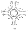
- the optical transistor contains four semiconductor lasers and two pairs of strip-shaped waveguides
- the longitudinal axes of each strip-shaped waveguide leading through central sections of each strip-shaped waveguide and in the region of the optical connection of the strip-shaped waveguides to the non-linear resonator with each adjacent end section of the strip-shaped waveguide form an angle of 45 ° and the adjacent end portions of the strip-shaped waveguide have four pairs of areas of mutual optical connection, which are equipped with control electrodes and are housed in pairs on two mutually perpendicular diametrical straight lines.
- the optical transistor as a component forms a matrix with the total number of inputs of 2n, where n is the number of cells of the switching matrices which are formed by a ring resonator which contains four lasers and four strip-shaped waveguides.
- the present invention allows to spatially concentrate the optical radiation of the input signals and the pump radiation of the lasers in the unitary element - the resonance ring, from which the output radiation is transmitted to optical contacts, - to work in two working areas: in the bistable and in the area of amplification of the optical signals smaller, (microwatt) sizes with a high (up to 104) coefficient of amplification, - To generate a high threshold sensitivity by the Presence of the sources of pumping - laser - is ensured, which keeps the system at the point of resonance triggering, - To control the output characteristics of the transistor by changing the optical characteristics of the non-linear resonator and laser, which leads to the expansion of the functional possibilities of the device and also offers the possibility of using it as an amplifier, as a pulse shaper, as a storage element, as a discriminator and as a limiter use, to re-emit the optical input signal to the optical output signal which has frequencies other than the input signal, the choice of the control voltage making it possible to digitally match the own frequencies of the
- the embodiment with four symmetrical optical contacts allows it to be used as a splitter, demultiplexor and switch for optical channels.
- Another variant guarantees the possibility of using it as a switching matrix with amplification.
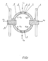
- the exemplary embodiment of an optical transistor shown in FIG. 1 contains two semiconductor lasers 1 on a common substrate, which are accommodated in a nonlinear ring resonator 2, and two strip-shaped light guides 3, each of which has an optical connection region A with the nonlinear ring resonator 2.
- the optical connection areas A are arranged opposite one another.
- the semiconductor lasers 1 are equipped with electrodes 4 for the power supply, each optical connection area A with a control electrode 5 and each section of the nonlinear ring resonator 2, which is located between the semiconductor laser 1 and corresponding optical connection areas A, with control electrodes 6.
- Mirrors 7 form the resonators of the semiconductor laser 1.
- the optical transistor works as follows: For the working range, which corresponds to the characteristic of the bistability, the current values i1 and i2 in the semiconductor lasers 1 and the voltages U1 and U2 on the control electrodes 5, 6 in the original state of the optical transistor when there is no optical (external ) Input signal such that the total intensity of the output radiation of the semiconductor laser 1 does not reach the threshold for the occurrence of the nonlinear effect in the material of the nonlinear ring resonator 2, the latter being in a state which is far from the resonance.
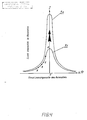
- This state of the optical transistor with regard to the light transmission from the input to the output corresponds to the point A on the curve R1 (Fig.
- n2 is the coefficient of nonlinearity of the material of the nonlinear ring resonator 2
- n0 the refraction coefficient in the absence of radiation.
- the above-mentioned bistable tearing off of the signal to be pumped in turn produces a drastic increase in the light intensity in the nonlinear ring resonator 2, which means an increase in the light intensity for the bistable cell "strip-shaped waveguide 3 - nonlinear ring resonator 2", which causes the transition of the optical transistor to the state from Point Q is circumscribed (Fig. 5), accelerated even more.
- the stable state of the device which corresponds to the said point of the work area, is maintained until the light intensity within the nonlinear ring resonator 2 is reduced to the size I min by the pulse reduction of the current values i 1 and i 2, which is necessary for the restoration of the original state the device (in the absence of external optical signals) is required.
- the nonlinear ring resonator 2 ensures both the interaction between the semiconductor lasers 1 and the joint work of the elementary ones bistable cells "strip-shaped waveguide 3 - nonlinear ring resonator 2".
- the symmetrical positioning of the lasers ensures that all optical inputs and outputs of the optical transistor are equivalent to the optical signals and that the half-rings of the nonlinear ring resonator 2 are inflated evenly.
- the conditions of the stability of the optical transistor correspond to the conditions of stability which apply to C3 lasers and other devices based on optically connected nonlinear resonators in which bistable optical elements are used.
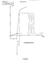
- K ampl. F (I in. ) (FIG. 6).
- the voltage values U1 and U2 and the strength of the optical input signal are such that the optical transistor does not yet pass into the bistable operating range in the case of the drastic increase in the light intensity within the nonlinear ring resonator 2, but rather operates as an optical amplifier with a gain factor of 103 to 104.
- FIG. 3 contains heterostructures Al x Ga 1-x As - GaAs - Al y Ga 1-y As (FIG. 3) located in the waveguide layer, the ring resonator 2 and the waveguide 3.
- Four semiconductor lasers 1 with electrodes 5 on the upper surface of the structure cross the ring resonator 2.
- Each of the waveguides 3 is optically connected to the ring resonator and over the area of the optical connection A1D2, A2B1, C2D1 and B2C1 control electrodes 6 are attached.
- a final electrode 13 is formed on the underside of the substrate (FIG. 3).
- the adjacent end portions of the strip-shaped waveguide 3 have four pairs of mutual optical connection areas - A1A2, B1B2, C1c2, D1D2.
- the transmission of the optical radiation in the connected directional coupler, for example A1A2 (Fig. 2) from one input of the waveguide, for example A1 to the other - A2 takes place in the absence of the control signal.
- A1A2 Fig. 2
- its length is critical, i.e. is such that the power is completely transmitted from one input of the waveguide to the other (for example from A1 to A2).
- this applies equally to any connected directional coupler as well as to the waveguides and ring resonators formed (for example waveguides A1D2 and section of the ring A1D2).
- the ring resonator 2 forms four pairs of bound directional couplers.
- the connection is maximum with precise resonance.
- the effect of the optical bistability is used, which makes it possible to obtain either a hysteresis dependency or a clear characteristic of the differential amplification of optical signals by the original detuning of the resonator.
- the second embodiment works as follows: in the event that there is no control signal at the control electrodes, the lasers are in the waiting working area, on the threshold of tearing off.
- the resonator is out of tune.
- An (any, for example A1) input of the waveguide 3 is given an optical signal which is to be amplified and further switched to any (for example D1) output.
- the radiation is pumped onto the input A2 of the waveguide 3 and due to the optical connection between the waveguide A2 and the ring resonator 2 in the latter and directed counterclockwise.
- This additional radiation leads to the process in the resonator 2 of the brightening of the medium in accordance with the dependency 1 and the property of the optical bistable cell "waveguide ring resonator".
- This brightening is expressed in that the resonator 2 approaches the precise resonance and the system changes into the resonance state.
- the directional couplers which are detected with feedback, express properties of the optical bistability and jump to the maximum output power at a certain input power. This transition becomes more active here due to the resonance properties of the ring resonator 2 and the presence Elements - the laser 1 - additionally initiated, the radiation of which is also subordinate to the effect of optical bistability.
- the maximum values of any output channel can exceed the input values by a dozen or a hundred times.
- the steepness of the characteristic "light-light” remains high enough so that sizes of 103-104 can be realized for the gain coefficient.
- the radiation Due to the optical connection of the resonance ring with the waveguides, the radiation is pumped around in the direction of C1, D1, B1 and through the connection between the waveguides in the direction of C2, D2, B2. Since the maximum connection between the ring 2 and the waveguides 3 is produced only by precise resonance by changing the refractive index in the resonator, the maximum values of the radiation are generated in the output. In this way, the signal given to input A 1 is initiated after amplification of the power from any output. For the generation of the amplified signal, for example at the output D2, electrical control signals are to be applied to the electrodes A1A2, C2D1, B2C1, A2B1, D2D1.
- the proposed device can perform the function of a storage device, i.e. be a memory cell.
- a storage device i.e. be a memory cell.
- Each input of the optical transistor can be used for the transmission of the optical storage pulse. Can be read from any output.
- the lasers 1 are located in the working area of the generation, minimal output can be given to any output that the corresponds to logical zero. For example, a pulse is given to the input, which is transmitted via the waveguide 3 of the directional coupler and the area of the connection A1D2 in the ring resonator.
- the additional radiation (in addition to the radiation from the lasers) in the resonator 2 will bring about processes which have already been described above: the radiation in the resonator becomes more intense due to the brightening of the medium and the resonance properties of the ring.
- the state of the memory cell can be read very easily from only one, for example from the C1 output: electrical control signals are applied to the electrodes A1D2, B2C1, A2B1.
- the state of logic one is maintained regardless of whether or not it has been read.
- the quenching takes place by the pulsed disconnection of the laser from the power source.
- the length of this pulse can be less than a picosecond.
- a structure based on solid three-component solutions in the GaAs-AlAs system is grown on the base made of GaAs using the epitaxy method.
- the couplers and the ring resonator are produced in the waveguide layer 14 by the ion implantation.
- Breggow laser mirrors are produced in the upper layer of the structure using the interference photo-etching process.
- the electrodes 5, 6, 10, 13 are manufactured on the upper surface of the structure.
- the electrodes 10 are multi-cell electrodes, 5 and 6 are electrically insulated electrodes.
- the lower electrode 13 represents a metallic plate on which the entire device is attached with the aid of an indium-based solder.
- Semiconductors from groups A3B5 and A2B6 as well as multicomponent structures can be used on the basis thereof in the manufacture of the switchover of optical channels.
- the switch of optical channels with the amplification of optical signals according to FIG. 2 can be regarded as an elementary cell for the construction of switching matrices and fields of larger dimensions.
- FIG. 7 shows a diagram of optical connections of the waveguides and the order of the ring conductors ⁇ and the ring resonators K, which are provided with four lasers 1 in the matrix with a total number of inputs of 32.
- the closed waveguide ⁇ optically connects the four ring resonators K.
- Switching the optical radiation from any input to any output can be done in different optical ways. So you can switch from A1 to C1 as follows: A1 - K1 - ⁇ - R3 - C2 - C1 or A1 - K1 - ⁇ - R2 - P3 - C1 or A1 - K1 - ⁇ - R4 - P3 - C2 - C1.
- the device depicted in FIG. 7 can also function as a matrix of a storage device. The specificity of such a memory matrix is that the excited "upper" state of the optical bistability of the memory can be generated by introducing an optical signal into any input and can be read at any output. The only thing that matters is to correctly select the algorithms for switching on electrical control pulses so that the state of the given cell on the given output is illuminated.
- the invention can be used in optical fiber systems for connecting and transmitting information, in schemes of integral optics and computer technology, and as an optical amplifier, as a pulse shaper, as an optical storage element, as a discriminator, as an optical limiter, as a switching element for optical channels, as an optical generator, as a branching device and as Demultiplexor can be used.
Landscapes
- Physics & Mathematics (AREA)
- General Physics & Mathematics (AREA)
- Nonlinear Science (AREA)
- Optics & Photonics (AREA)
- Semiconductor Lasers (AREA)
- Optical Integrated Circuits (AREA)
- Light Receiving Elements (AREA)
- Solid State Image Pick-Up Elements (AREA)
- Recrystallisation Techniques (AREA)
Applications Claiming Priority (2)
| Application Number | Priority Date | Filing Date | Title |
|---|---|---|---|
| SU4619989 | 1988-12-13 | ||
| SU884619989A SU1755246A1 (ru) | 1988-12-13 | 1988-12-13 | Оптический транзистор |
Publications (2)
| Publication Number | Publication Date |
|---|---|
| EP0373541A2 true EP0373541A2 (fr) | 1990-06-20 |
| EP0373541A3 EP0373541A3 (fr) | 1991-01-16 |
Family
ID=21415028
Family Applications (1)
| Application Number | Title | Priority Date | Filing Date |
|---|---|---|---|
| EP19890122734 Withdrawn EP0373541A3 (fr) | 1988-12-13 | 1989-12-09 | Transistor optique |
Country Status (6)
| Country | Link |
|---|---|
| US (1) | US5001523A (fr) |
| EP (1) | EP0373541A3 (fr) |
| JP (1) | JPH02276285A (fr) |
| HU (1) | HUT55569A (fr) |
| SU (1) | SU1755246A1 (fr) |
| YU (1) | YU234889A (fr) |
Cited By (1)
| Publication number | Priority date | Publication date | Assignee | Title |
|---|---|---|---|---|
| CN102226862A (zh) * | 2006-02-14 | 2011-10-26 | 科维特克有限公司 | 使用非线性元件的全光逻辑门 |
Families Citing this family (25)
| Publication number | Priority date | Publication date | Assignee | Title |
|---|---|---|---|---|
| US5123027A (en) * | 1990-06-13 | 1992-06-16 | Northrop Corporation | Regenerative passive resonator |
| FR2692374B1 (fr) * | 1992-06-15 | 1994-07-29 | France Telecom | Procede et dispositif de modulation et d'amplification de faisceaux lumineux. |
| RU2099762C1 (ru) * | 1992-07-06 | 1997-12-20 | Фирма "Самсунг Электроникс Ко., Лтд." | Оптический регенератор |
| RU2105389C1 (ru) * | 1992-07-06 | 1998-02-20 | Самсунг Электроникс Ко., Лтд. | Полностью оптический регенератор |
| US5459800A (en) * | 1992-07-30 | 1995-10-17 | Matsushita Electric Industrial Co., Ltd. | Optical modulation device and method of driving the same |
| RU2097815C1 (ru) * | 1993-02-12 | 1997-11-27 | Фирма "Самсунг Электроникс Ко., Лтд." | Оптический процессор |
| RU2111520C1 (ru) * | 1993-07-21 | 1998-05-20 | Фирма "Самсунг Электроникс Ко., Лтд." | Оптический процессор с бустерным выходом |
| RU2107938C1 (ru) * | 1993-07-21 | 1998-03-27 | Самсунг Электроникс Ко., Лтд. | Нелинейный оптический транзистор |
| US5926496A (en) * | 1995-05-25 | 1999-07-20 | Northwestern University | Semiconductor micro-resonator device |
| US7120338B2 (en) * | 2001-09-10 | 2006-10-10 | California Institute Of Technology | Tuning the index of a waveguide structure |
| US6834152B2 (en) * | 2001-09-10 | 2004-12-21 | California Institute Of Technology | Strip loaded waveguide with low-index transition layer |
| US7082235B2 (en) * | 2001-09-10 | 2006-07-25 | California Institute Of Technology | Structure and method for coupling light between dissimilar waveguides |
| US7010208B1 (en) | 2002-06-24 | 2006-03-07 | Luxtera, Inc. | CMOS process silicon waveguides |
| US7315679B2 (en) * | 2004-06-07 | 2008-01-01 | California Institute Of Technology | Segmented waveguide structures |
| US7826688B1 (en) | 2005-10-21 | 2010-11-02 | Luxtera, Inc. | Enhancing the sensitivity of resonant optical modulating and switching devices |
| US7394958B2 (en) * | 2006-02-14 | 2008-07-01 | Coveytech, Llc | All-optical logic gates using nonlinear elements-claim set II |
| US7263262B1 (en) * | 2006-02-14 | 2007-08-28 | Coveytech, Llc | All-optical logic gates using nonlinear elements-claim set VI |
| US20070189703A1 (en) * | 2006-02-14 | 2007-08-16 | Coveytech, Llc | All-optical logic gates using nonlinear elements-claim set I |
| US7409131B2 (en) * | 2006-02-14 | 2008-08-05 | Coveytech, Llc | All-optical logic gates using nonlinear elements—claim set V |
| US7428359B2 (en) * | 2006-02-14 | 2008-09-23 | Coveytech, Llc | All-optical logic gates using nonlinear elements—claim set IV |
| US7664355B2 (en) * | 2006-02-14 | 2010-02-16 | Coveytech Llc | All-optical gates using nonlinear elements-claim set III |
| US20070206897A1 (en) * | 2006-03-03 | 2007-09-06 | Dr. Shaowen Song | N-nary optical semiconductor transistor and an optical AND gate |
| US8379300B2 (en) * | 2008-02-19 | 2013-02-19 | Nec Corporation | Wavelength-variable light source with dual resonator loop circuit |
| CA2927537A1 (fr) * | 2013-10-15 | 2015-04-23 | Coriant Advanced Technology, LLC | Fonctionnement et stabilisation d'emetteurs mod-mux a multiplexage par repartition en longueur d'onde (wdm) bases sur des micro-anneaux en silicium |
| CN104280899B (zh) * | 2014-10-27 | 2016-11-23 | 山东大学 | 基于微环谐振腔的硅基热光调制器 |
Citations (3)
| Publication number | Priority date | Publication date | Assignee | Title |
|---|---|---|---|---|
| US3760297A (en) * | 1972-01-20 | 1973-09-18 | Int Standard Electric Corp | Laser to optical fiber coupling |
| US4695121A (en) * | 1985-01-28 | 1987-09-22 | Polaroid Corporation | Integrated optic resonant structres and fabrication method |
| EP0279520A2 (fr) * | 1987-01-21 | 1988-08-24 | Kokusai Denshin Denwa Kabushiki Kaisha | Commutateur à guides d'ondes optiques |
Family Cites Families (7)
| Publication number | Priority date | Publication date | Assignee | Title |
|---|---|---|---|---|
| US3610731A (en) * | 1969-05-19 | 1971-10-05 | Bell Telephone Labor Inc | Bistable optical circuit using saturable absorber within a resonant cavity |
| US3849740A (en) * | 1973-05-01 | 1974-11-19 | Westinghouse Electric Corp | Integrated optical and/or gate |
| BE859530A (fr) * | 1976-10-15 | 1978-02-01 | Western Electric Co | Interferometre non lineaire |
| FR2464498A1 (fr) * | 1979-08-30 | 1981-03-06 | Carenco Alain | Dispositif optique bistable integre |
| US4775214A (en) * | 1983-12-21 | 1988-10-04 | Rosemount Inc. | Wavelength coded resonant optical sensor |
| US4632518A (en) * | 1984-07-31 | 1986-12-30 | Hughes Aircraft Company | Phase insensitive optical logic gate device |
| GB2210991B (en) * | 1987-10-09 | 1991-09-11 | Oki Electric Ind Co Ltd | Optical switch matrix |
-
1988
- 1988-12-13 SU SU884619989A patent/SU1755246A1/ru active
-
1989
- 1989-12-09 EP EP19890122734 patent/EP0373541A3/fr not_active Withdrawn
- 1989-12-11 US US07/449,529 patent/US5001523A/en not_active Expired - Fee Related
- 1989-12-12 YU YU02348/89A patent/YU234889A/xx unknown
- 1989-12-13 HU HU896517A patent/HUT55569A/hu unknown
- 1989-12-13 JP JP1321591A patent/JPH02276285A/ja active Pending
Patent Citations (3)
| Publication number | Priority date | Publication date | Assignee | Title |
|---|---|---|---|---|
| US3760297A (en) * | 1972-01-20 | 1973-09-18 | Int Standard Electric Corp | Laser to optical fiber coupling |
| US4695121A (en) * | 1985-01-28 | 1987-09-22 | Polaroid Corporation | Integrated optic resonant structres and fabrication method |
| EP0279520A2 (fr) * | 1987-01-21 | 1988-08-24 | Kokusai Denshin Denwa Kabushiki Kaisha | Commutateur à guides d'ondes optiques |
Cited By (2)
| Publication number | Priority date | Publication date | Assignee | Title |
|---|---|---|---|---|
| CN102226862A (zh) * | 2006-02-14 | 2011-10-26 | 科维特克有限公司 | 使用非线性元件的全光逻辑门 |
| EP2711772A1 (fr) * | 2006-02-14 | 2014-03-26 | Coveytech, LLC | Portes logiques entièrement optiques utilisant des éléments non linéaires |
Also Published As
| Publication number | Publication date |
|---|---|
| US5001523A (en) | 1991-03-19 |
| YU234889A (en) | 1991-10-31 |
| HU896517D0 (en) | 1990-02-28 |
| HUT55569A (en) | 1991-05-28 |
| EP0373541A3 (fr) | 1991-01-16 |
| SU1755246A1 (ru) | 1992-08-15 |
| JPH02276285A (ja) | 1990-11-13 |
Similar Documents
| Publication | Publication Date | Title |
|---|---|---|
| EP0373541A2 (fr) | Transistor optique | |
| DE3789437T2 (de) | Optischer Schalter. | |
| DE68924996T2 (de) | Optische Quanten-Interferenz-Vorrichtung. | |
| DE69826088T2 (de) | Lasersender mit verminderter Verzerrung | |
| DE102006045102B4 (de) | Elektro-optisches Hochindexkontrast-Wellenleiter-Bauelement | |
| DE69420628T2 (de) | Rein optische Vorrichtung | |
| DE69223463T2 (de) | Optische Halbleiter-Wellenleitervorrichtung und ihr Herstellungsverfahren | |
| DE69409539T2 (de) | Optische schalteinrichtung | |
| DE69122939T2 (de) | Optische Steuervorrichtung | |
| DE69022257T2 (de) | Optischer Halbleiterschalter und Schaltermatrix. | |
| DE69412738T2 (de) | Verspannte Quantumwellstruktur mit variabler Polarisationsabhängigkeit und optische Vorrichtung mit dieser verspannten Quantumwellstruktur | |
| DE4327102A1 (de) | Abstimmbares optisches Filter | |
| DE68924949T2 (de) | Nichtlineare optische Vorrichtung. | |
| DE68906601T2 (de) | Symmetrischer integrierter Verstärker mit gesteuerter Offset-Gleichspannung. | |
| DE3874364T2 (de) | Optischer wellenleiterschalter. | |
| DE3883492T2 (de) | Verfahren zur Anordnung eines polarisationsrichtenden optoelektronischen Schalters und ein Schalter dafür. | |
| EP0569353A1 (fr) | Structures guides d'ondes en niobate de lithium a dopage en terres rares. | |
| DE69801709T2 (de) | Optisches Übertragungssystem mit dynamischer Kompensation der übertragenen Leistung | |
| DE3590607C2 (de) | Optischer Richtungskoppler | |
| DE69114282T2 (de) | Optischer signalregenerator und optisches übertragungssystem, das diesen benutzt. | |
| DE69528576T2 (de) | Hochleistungs-wellenleitermodulator vom absorptionstyp | |
| DE60314745T2 (de) | Integriertes optisches Verstärkungs- und Schaltmodul auf Halbleiterbasis | |
| DE69600573T2 (de) | Optischer verstärker | |
| DE102020124034A1 (de) | Optische Matrixmultiplikationseinheit für ein optoelektronisches System zur Bildung eines künstlichen neuralen Netzes | |
| DE60109045T2 (de) | Integrierte optische Weglenkungs- und Wellenlängenkonversionsmatrix |
Legal Events
| Date | Code | Title | Description |
|---|---|---|---|
| PUAI | Public reference made under article 153(3) epc to a published international application that has entered the european phase |
Free format text: ORIGINAL CODE: 0009012 |
|
| AK | Designated contracting states |
Kind code of ref document: A2 Designated state(s): AT BE CH DE FR GB IT LI NL SE |
|
| PUAL | Search report despatched |
Free format text: ORIGINAL CODE: 0009013 |
|
| AK | Designated contracting states |
Kind code of ref document: A3 Designated state(s): AT BE CH DE FR GB IT LI NL SE |
|
| RHK1 | Main classification (correction) |
Ipc: G02F 3/00 |
|
| 17P | Request for examination filed |
Effective date: 19910410 |
|
| 17Q | First examination report despatched |
Effective date: 19930707 |
|
| STAA | Information on the status of an ep patent application or granted ep patent |
Free format text: STATUS: THE APPLICATION IS DEEMED TO BE WITHDRAWN |
|
| 18D | Application deemed to be withdrawn |
Effective date: 19931119 |