EP0279520A2 - Commutateur à guides d'ondes optiques - Google Patents
Commutateur à guides d'ondes optiques Download PDFInfo
- Publication number
- EP0279520A2 EP0279520A2 EP88300488A EP88300488A EP0279520A2 EP 0279520 A2 EP0279520 A2 EP 0279520A2 EP 88300488 A EP88300488 A EP 88300488A EP 88300488 A EP88300488 A EP 88300488A EP 0279520 A2 EP0279520 A2 EP 0279520A2
- Authority
- EP
- European Patent Office
- Prior art keywords
- light
- side optical
- optical
- optical waveguides
- optical waveguide
- Prior art date
- Legal status (The legal status is an assumption and is not a legal conclusion. Google has not performed a legal analysis and makes no representation as to the accuracy of the status listed.)
- Granted
Links
- 230000003287 optical effect Effects 0.000 title claims abstract description 80
- 239000000463 material Substances 0.000 claims abstract description 27
- 230000005284 excitation Effects 0.000 description 15
- 238000010521 absorption reaction Methods 0.000 description 9
- 238000006243 chemical reaction Methods 0.000 description 8
- 238000002310 reflectometry Methods 0.000 description 5
- 239000004065 semiconductor Substances 0.000 description 4
- 238000002347 injection Methods 0.000 description 3
- 239000007924 injection Substances 0.000 description 3
- 238000000034 method Methods 0.000 description 3
- 238000000862 absorption spectrum Methods 0.000 description 2
- 230000005540 biological transmission Effects 0.000 description 2
- 230000007423 decrease Effects 0.000 description 2
- 230000003247 decreasing effect Effects 0.000 description 2
- 238000011161 development Methods 0.000 description 2
- 230000000694 effects Effects 0.000 description 2
- 238000005516 engineering process Methods 0.000 description 2
- 238000003780 insertion Methods 0.000 description 2
- 230000037431 insertion Effects 0.000 description 2
- 239000013307 optical fiber Substances 0.000 description 2
- 229920006395 saturated elastomer Polymers 0.000 description 2
- 229910000980 Aluminium gallium arsenide Inorganic materials 0.000 description 1
- 230000006978 adaptation Effects 0.000 description 1
- 238000013459 approach Methods 0.000 description 1
- 230000008878 coupling Effects 0.000 description 1
- 238000010168 coupling process Methods 0.000 description 1
- 238000005859 coupling reaction Methods 0.000 description 1
- 239000013078 crystal Substances 0.000 description 1
- 230000007547 defect Effects 0.000 description 1
- 238000010586 diagram Methods 0.000 description 1
- 239000006185 dispersion Substances 0.000 description 1
- 230000031700 light absorption Effects 0.000 description 1
- 238000004519 manufacturing process Methods 0.000 description 1
- 230000005693 optoelectronics Effects 0.000 description 1
Images


Classifications
-
- G—PHYSICS
- G02—OPTICS
- G02B—OPTICAL ELEMENTS, SYSTEMS OR APPARATUS
- G02B6/00—Light guides; Structural details of arrangements comprising light guides and other optical elements, e.g. couplings
- G02B6/24—Coupling light guides
- G02B6/26—Optical coupling means
- G02B6/28—Optical coupling means having data bus means, i.e. plural waveguides interconnected and providing an inherently bidirectional system by mixing and splitting signals
- G02B6/293—Optical coupling means having data bus means, i.e. plural waveguides interconnected and providing an inherently bidirectional system by mixing and splitting signals with wavelength selective means
- G02B6/29331—Optical coupling means having data bus means, i.e. plural waveguides interconnected and providing an inherently bidirectional system by mixing and splitting signals with wavelength selective means operating by evanescent wave coupling
- G02B6/29335—Evanescent coupling to a resonator cavity, i.e. between a waveguide mode and a resonant mode of the cavity
- G02B6/29338—Loop resonators
-
- G—PHYSICS
- G02—OPTICS
- G02F—OPTICAL DEVICES OR ARRANGEMENTS FOR THE CONTROL OF LIGHT BY MODIFICATION OF THE OPTICAL PROPERTIES OF THE MEDIA OF THE ELEMENTS INVOLVED THEREIN; NON-LINEAR OPTICS; FREQUENCY-CHANGING OF LIGHT; OPTICAL LOGIC ELEMENTS; OPTICAL ANALOGUE/DIGITAL CONVERTERS
- G02F1/00—Devices or arrangements for the control of the intensity, colour, phase, polarisation or direction of light arriving from an independent light source, e.g. switching, gating or modulating; Non-linear optics
- G02F1/35—Non-linear optics
- G02F1/3515—All-optical modulation, gating, switching, e.g. control of a light beam by another light beam
Definitions
- the present invention relates to an optical switch for switching the propagation path of an optical signal and, more particularly, to an optical waveguide switch which utilizes light as control energy for triggering its switching operation.
- this optical switch has the defects of complexity in its manufacture, low reliability and an increase in cross-talk by electromagnetic interference in the electronic circuit during high-speed operation.
- the other optical switch is one that switches an optical signal without conversion to an electric signal, and this switch is termed an O/O type.
- these optical switches rely on electric energy such as a voltage and a current for switching the optical signal, they have to perform the O/E (opto-elelctro) conversion of a control signal superimposed on the optical signal.
- An object of the present invention is to provide an optical waveguide switch which permits the switching of an optical signal without the necessity of its opto-electro conversion.
- Characteristic features of the present invention reside in that the switching section is formed using a non-linear material whose refractive index varies with the intensity of irradiation light and a positive feedback loop is provided in the waveguide section so that the optical signal is switched intact.
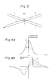
- Figs. 1 and 2 show, in elevation, known optical switches.
- the optical switch depicted in Fig. 1 employs directional couplers. By applying a voltage as a control signal to a switching section the refractive indices are varied so that the phase matching condition between two waveguides is satisfied or not satisfied for switching incident light between them.
- the optical switch in Fig. 2 employs a current as a control signal. By injecting a current into the intersecting portion of two waveguides centrally thereof their refractive indices are varied with the resulting carrier density, whereby incident light is totally reflected and switched from one waveguide to the other.
- optical switches do not involve the aforementioned O/E and E/O conversions of the optical signal, and hence have advantages in that they are simple in structure and capable of switching without impairing the wide band property of the optical signal.
- these optical switches rely on electric energy such as a voltage and a current, for switching the optical signal, they have to perform the O/E conversion of a control signal superimposed on the optical signal, and accordingly they are inevitably provided with a photo-detector and circuit elements therefor.
- the optically non-linear material 3 has an absorption spectrum based on the resonance of the levels of atoms or molecules forming it, as shown in Fig. 4A, and its absorption coefficient is related to the refractive index by the Kramers-Kronig relations, as shown in Fig. 4B.
- Fig. 4A absorption spectrum based on the resonance of the levels of atoms or molecules forming it
- Fig. 4B absorption coefficient is related to the refractive index by the Kramers-Kronig relations
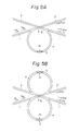
- Figs. 5A and 5B illustrate an embodiment of the optical waveguide switch of the present invention, in which guided light, effective in practical applications, is used as irradiation light (hereinafter referred to as excitation light).
- reference numerals 1 and 2 indicate incoming side waveguides, 1 ⁇ and 2 ⁇ outgoing side reflection and transmission waveguides, 3 a non-linear material, 4 a feedback waveguide, 5 an optical amplifier and 6 a semi-conductor material other than the non-linear material 3.
- the incoming and outgoing waveguides 1 and 1 ⁇ and the feedback waveguide 4 are formed to constitute a loop as shown.
- the excited light P ex of a longer wavelength than the absorption centre wavelength ⁇ 0 is incident to the incoming side waveguide 1, it is absorbed by the non-linear material 3, in consequence of which the absorption coefficient of the non-linear material 3 decreases as shown in Fig. 4 and its refractive index also lowers correspondingly. Since the refractive indices of the non-linear material 3 and the surrounding material 6 are selected such that they are equal to each other in the absence of the excitation light P ex , the reflectivity at the interface between them is zero. When a refractive index difference has occurred upon incidence of light P ex , the reflectivity R starts to increase and a portion of the light P ex is reflected toward the outgoing side waveguide 1 ⁇ .
- a portion of the reflected light P0 is branched into the feedback waveguide 4, in which it is amplified by the optical amplifier 5 and the amplified light is led again to the incoming side waveguide 1, thereafter being absorbed by the non-linear material 3.
- This process further promotes the reduction of the absorption coefficient of the non-linear material 3, and consequently the reflected light P0 also increases. That is to say, by the presence of the feedback waveguide 4 a positive feedback is caused in the absorption and refractive index variation of the non-linear material 3 and the abovementioned process is repeated, by which the feedback effect is markedly accelerated, reducing the refractive index to such an extent that total reflection will ultimately occur.
- Fig. 7A shows the relationship between the excitation light P ex and the output light P o from the waveguide 1 ⁇ .
- the output light P o shows such bistability as depicted in Fig. 7B.
- each output P o can be switched from its high level (the total reflection state) to its low level (the zero reflection state) by holding the excitation light P ex at the centre P exb of the bistable loop and adding thereto incremental or decremental pulses as shown.
- the switching can be achieved with the excitation light P ex alone, and a direct current can be used as the current I al .
- the Bragg reflection type branching filter 7 is formed so that its Bragg wavelength may be equal to ⁇ ex .
- the feedback waveguide 4 can be used for each of the incoming side waveguides 1 and 2.
- the waveguides can be formed by ridge, rib and buried structures, using semiconductors such as the In GaAsP and the AlGaAs crystal systems.
- the optically non-linear material 3 is used in its switching section to provide the zero reflection or total reflection state, depending on the intensity of light, and at least one feedback waveguide 4 is provided for controlling the optically non-linear material 3 to permit switching of an optical signal even in case of a feeble excitation light.
Landscapes
- Physics & Mathematics (AREA)
- Nonlinear Science (AREA)
- General Physics & Mathematics (AREA)
- Optics & Photonics (AREA)
- Optical Integrated Circuits (AREA)
Applications Claiming Priority (2)
| Application Number | Priority Date | Filing Date | Title |
|---|---|---|---|
| JP9942/87 | 1987-01-21 | ||
| JP62009942A JPH0721599B2 (ja) | 1987-01-21 | 1987-01-21 | 導波路型光スイツチ |
Publications (3)
| Publication Number | Publication Date |
|---|---|
| EP0279520A2 true EP0279520A2 (fr) | 1988-08-24 |
| EP0279520A3 EP0279520A3 (en) | 1988-08-31 |
| EP0279520B1 EP0279520B1 (fr) | 1992-09-09 |
Family
ID=11734058
Family Applications (1)
| Application Number | Title | Priority Date | Filing Date |
|---|---|---|---|
| EP88300488A Expired EP0279520B1 (fr) | 1987-01-21 | 1988-01-21 | Commutateur à guides d'ondes optiques |
Country Status (4)
| Country | Link |
|---|---|
| US (1) | US4805975A (fr) |
| EP (1) | EP0279520B1 (fr) |
| JP (1) | JPH0721599B2 (fr) |
| DE (1) | DE3874364T2 (fr) |
Cited By (2)
| Publication number | Priority date | Publication date | Assignee | Title |
|---|---|---|---|---|
| EP0373541A2 (fr) * | 1988-12-13 | 1990-06-20 | Tsentr Nauchno-Tekhnicheskogo Tvorchestva Molodezhi " Linax" | Transistor optique |
| EP0857314A1 (fr) * | 1995-10-27 | 1998-08-12 | Arroyo Optics Inc. | Dispositifs optiques selectifs en longueurs d'ondes |
Families Citing this family (17)
| Publication number | Priority date | Publication date | Assignee | Title |
|---|---|---|---|---|
| JP2764263B2 (ja) * | 1987-09-16 | 1998-06-11 | セイコーインスツルメンツ株式会社 | 波長フィルタ |
| JPH0769549B2 (ja) * | 1987-10-22 | 1995-07-31 | 国際電信電話株式会社 | 光駆動形スイッチ |
| GB8728854D0 (en) * | 1987-12-10 | 1988-01-27 | British Telecomm | Optical device |
| US5136669A (en) * | 1991-03-15 | 1992-08-04 | Sperry Marine Inc. | Variable ratio fiber optic coupler optical signal processing element |
| JPH05196973A (ja) * | 1991-09-12 | 1993-08-06 | Sumitomo Electric Ind Ltd | 光スイッチ |
| US5243676A (en) * | 1991-09-19 | 1993-09-07 | E. I. Du Pont De Nemours And Company | Segmented waveguides having selected Bragg reflection characteristics |
| DE4200397C1 (fr) * | 1992-01-10 | 1993-03-04 | Imm Institut Fuer Mikrotechnik Gmbh, 6500 Mainz, De | |
| DE4200396C1 (fr) * | 1992-01-10 | 1993-02-04 | Imm Institut Fuer Mikrotechnik Gmbh, 6500 Mainz, De | |
| DE69423548T2 (de) * | 1993-07-21 | 2000-09-14 | At & T Corp | Verbesserter Faserschleifenreflektor zum Zeitdemultiplexen |
| US5493433A (en) * | 1994-03-02 | 1996-02-20 | Trustees Of Princeton University | Terahertz optical asymmetric demultiplexer |
| IL119006A (en) | 1996-08-04 | 2001-04-30 | B G Negev Technologies And App | Optical filters with adjustable stay line |
| US6697548B2 (en) * | 2000-12-18 | 2004-02-24 | Evident Technologies | Fabry-perot opitcal switch having a saturable absorber |
| US6697542B2 (en) * | 2000-12-29 | 2004-02-24 | Lucent Technologies Inc. | Integrated optical switches using nonlinear optical media |
| US6766083B2 (en) * | 2001-10-16 | 2004-07-20 | International Business Machines Corporation | Tunable coupler device and optical filter |
| JP3692354B2 (ja) * | 2002-12-26 | 2005-09-07 | 独立行政法人科学技術振興機構 | 電磁波周波数フィルタ |
| US7110154B2 (en) * | 2004-06-10 | 2006-09-19 | Clemson University | Plasmon-photon coupled optical devices |
| US7447397B1 (en) | 2004-06-14 | 2008-11-04 | Dynamic Method Enterprises Limited | Optical switch matrix |
Citations (3)
| Publication number | Priority date | Publication date | Assignee | Title |
|---|---|---|---|---|
| EP0105693A2 (fr) * | 1982-09-30 | 1984-04-18 | Fujitsu Limited | Commutateur optique bipolaire contrôlé en tension utilisant des guides d'ondes entrecroisés |
| WO1984003363A1 (fr) * | 1983-02-28 | 1984-08-30 | American Telephone & Telegraph | Dispositif optique non lineaire |
| EP0207725A1 (fr) * | 1985-06-26 | 1987-01-07 | THE GENERAL ELECTRIC COMPANY, p.l.c. | Commutateur optique |
Family Cites Families (5)
| Publication number | Priority date | Publication date | Assignee | Title |
|---|---|---|---|---|
| US4382660A (en) * | 1976-06-16 | 1983-05-10 | Massachusetts Institute Of Technology | Optical transistors and logic circuits embodying the same |
| US4211467A (en) * | 1978-01-13 | 1980-07-08 | Bell Telephone Laboratories, Incorporated | Optically-controlled two-channel integrated optical switch |
| FR2533714A1 (fr) * | 1982-09-28 | 1984-03-30 | Thomson Csf | Dispositif coupleur optique integre non lineaire et oscillateur parametrique comprenant un tel dispositif |
| US4626075A (en) * | 1983-01-03 | 1986-12-02 | At&T Bell Laboratories | Light beam applied to a layered semiconductor structure is controlled by another light beam |
| US4507776A (en) * | 1983-09-12 | 1985-03-26 | At&T Bell Laboratories | Nonlinear all-optical time division multiplexer and demultiplexer |
-
1987
- 1987-01-21 JP JP62009942A patent/JPH0721599B2/ja not_active Expired - Fee Related
-
1988
- 1988-01-13 US US07/143,820 patent/US4805975A/en not_active Expired - Lifetime
- 1988-01-21 DE DE8888300488T patent/DE3874364T2/de not_active Expired - Fee Related
- 1988-01-21 EP EP88300488A patent/EP0279520B1/fr not_active Expired
Patent Citations (3)
| Publication number | Priority date | Publication date | Assignee | Title |
|---|---|---|---|---|
| EP0105693A2 (fr) * | 1982-09-30 | 1984-04-18 | Fujitsu Limited | Commutateur optique bipolaire contrôlé en tension utilisant des guides d'ondes entrecroisés |
| WO1984003363A1 (fr) * | 1983-02-28 | 1984-08-30 | American Telephone & Telegraph | Dispositif optique non lineaire |
| EP0207725A1 (fr) * | 1985-06-26 | 1987-01-07 | THE GENERAL ELECTRIC COMPANY, p.l.c. | Commutateur optique |
Non-Patent Citations (1)
| Title |
|---|
| JOURNAL OF APPLIED PHYSICS, vol. 58, no. 12, December 1985, pages R57-78, New York, US; G.I. STEGEMAN et al. : "Nonlinear integrated optics" * |
Cited By (3)
| Publication number | Priority date | Publication date | Assignee | Title |
|---|---|---|---|---|
| EP0373541A2 (fr) * | 1988-12-13 | 1990-06-20 | Tsentr Nauchno-Tekhnicheskogo Tvorchestva Molodezhi " Linax" | Transistor optique |
| EP0373541A3 (fr) * | 1988-12-13 | 1991-01-16 | Tsentr Nauchno-Tekhnicheskogo Tvorchestva Molodezhi " Linax" | Transistor optique |
| EP0857314A1 (fr) * | 1995-10-27 | 1998-08-12 | Arroyo Optics Inc. | Dispositifs optiques selectifs en longueurs d'ondes |
Also Published As
| Publication number | Publication date |
|---|---|
| JPH0721599B2 (ja) | 1995-03-08 |
| EP0279520B1 (fr) | 1992-09-09 |
| JPS63179337A (ja) | 1988-07-23 |
| US4805975A (en) | 1989-02-21 |
| DE3874364T2 (de) | 1993-01-14 |
| EP0279520A3 (en) | 1988-08-31 |
| DE3874364D1 (de) | 1992-10-15 |
Similar Documents
| Publication | Publication Date | Title |
|---|---|---|
| EP0279520B1 (fr) | Commutateur à guides d'ondes optiques | |
| JP2637531B2 (ja) | 光スイッチ | |
| CA1178703A (fr) | Organe optique de coupure | |
| CA1298388C (fr) | Dispositif optique symetrique | |
| CA2363630C (fr) | Commutateurs optiques integres faisant appel a des milieux optiques non lineaires | |
| CA2128839C (fr) | Modulateurs optiques servant d'isolants optiques integres monolithiques | |
| Korotky et al. | 4-Gb/s transmission experiment over 117 km of optical fiber using a Ti: LiNbO 3 external modulator | |
| EP1499921A1 (fr) | Modulateur optique | |
| CA2255450C (fr) | Modulateur optique faisant appel a un isolateur et emetteur optique incorporant un tel modulateur | |
| EP0527871B1 (fr) | Regenerateur de signal optique et systeme de communication optique l'incorporant | |
| US5016960A (en) | Hybrid optical Y-junction | |
| WO1995022774A1 (fr) | Modulateur a absorption pour guide d'ondes a forte puissance | |
| US5706383A (en) | Active noise suppressor for multichannel optical systems | |
| GB2227854A (en) | Integrated optics asymmetric y-coupler | |
| EP0313388B1 (fr) | Commutateur déclenché par de la lumière | |
| US6760141B2 (en) | Semiconductor optical modulator and semiconductor optical device | |
| CA1295684C (fr) | Emetteur reflex pour systeme de communication bidirectionnel a guides de lumiere | |
| JPH09269428A (ja) | 反射戻り光補償回路 | |
| JP2609610B2 (ja) | 光バイパススイッチモジュール | |
| GB2378525A (en) | Optic system | |
| US6271954B1 (en) | Waveguide absorption modulator with integral optical isolator | |
| Streifer et al. | Integrated interferometric reflector | |
| Deborgies et al. | New concepts for millimetre wave optical links | |
| Daryoush | Microwave Photonics in Dual-Use Military Systems–A Personal Perspective | |
| ITO et al. | Wavelength bandwidth of plasma dispersion effect total reflection type optical switches |
Legal Events
| Date | Code | Title | Description |
|---|---|---|---|
| PUAI | Public reference made under article 153(3) epc to a published international application that has entered the european phase |
Free format text: ORIGINAL CODE: 0009012 |
|
| PUAL | Search report despatched |
Free format text: ORIGINAL CODE: 0009013 |
|
| AK | Designated contracting states |
Kind code of ref document: A2 Designated state(s): DE FR GB |
|
| AK | Designated contracting states |
Kind code of ref document: A3 Designated state(s): DE FR GB |
|
| 17P | Request for examination filed |
Effective date: 19881013 |
|
| 17Q | First examination report despatched |
Effective date: 19900813 |
|
| GRAA | (expected) grant |
Free format text: ORIGINAL CODE: 0009210 |
|
| AK | Designated contracting states |
Kind code of ref document: B1 Designated state(s): DE FR GB |
|
| REF | Corresponds to: |
Ref document number: 3874364 Country of ref document: DE Date of ref document: 19921015 |
|
| ET | Fr: translation filed | ||
| PLBE | No opposition filed within time limit |
Free format text: ORIGINAL CODE: 0009261 |
|
| STAA | Information on the status of an ep patent application or granted ep patent |
Free format text: STATUS: NO OPPOSITION FILED WITHIN TIME LIMIT |
|
| 26N | No opposition filed | ||
| PGFP | Annual fee paid to national office [announced via postgrant information from national office to epo] |
Ref country code: GB Payment date: 20011214 Year of fee payment: 15 |
|
| PGFP | Annual fee paid to national office [announced via postgrant information from national office to epo] |
Ref country code: DE Payment date: 20011217 Year of fee payment: 15 |
|
| PGFP | Annual fee paid to national office [announced via postgrant information from national office to epo] |
Ref country code: FR Payment date: 20011226 Year of fee payment: 15 |
|
| REG | Reference to a national code |
Ref country code: GB Ref legal event code: IF02 |
|
| PG25 | Lapsed in a contracting state [announced via postgrant information from national office to epo] |
Ref country code: GB Free format text: LAPSE BECAUSE OF NON-PAYMENT OF DUE FEES Effective date: 20030121 |
|
| PG25 | Lapsed in a contracting state [announced via postgrant information from national office to epo] |
Ref country code: DE Free format text: LAPSE BECAUSE OF NON-PAYMENT OF DUE FEES Effective date: 20030801 |
|
| GBPC | Gb: european patent ceased through non-payment of renewal fee | ||
| PG25 | Lapsed in a contracting state [announced via postgrant information from national office to epo] |
Ref country code: FR Free format text: LAPSE BECAUSE OF NON-PAYMENT OF DUE FEES Effective date: 20030930 |
|
| REG | Reference to a national code |
Ref country code: FR Ref legal event code: ST |