EP0372473A2 - Funkrufempfänger - Google Patents
Funkrufempfänger Download PDFInfo
- Publication number
- EP0372473A2 EP0372473A2 EP89122380A EP89122380A EP0372473A2 EP 0372473 A2 EP0372473 A2 EP 0372473A2 EP 89122380 A EP89122380 A EP 89122380A EP 89122380 A EP89122380 A EP 89122380A EP 0372473 A2 EP0372473 A2 EP 0372473A2
- Authority
- EP
- European Patent Office
- Prior art keywords
- signal
- preamble
- synchronization
- address
- detection
- Prior art date
- Legal status (The legal status is an assumption and is not a legal conclusion. Google has not performed a legal analysis and makes no representation as to the accuracy of the status listed.)
- Granted
Links
- 238000001514 detection method Methods 0.000 claims abstract description 61
- 230000001360 synchronised effect Effects 0.000 claims description 4
- 238000010586 diagram Methods 0.000 description 10
- 241000486634 Bena Species 0.000 description 2
- 241000905510 Scena Species 0.000 description 2
- PCHPORCSPXIHLZ-UHFFFAOYSA-N diphenhydramine hydrochloride Chemical compound [Cl-].C=1C=CC=CC=1C(OCC[NH+](C)C)C1=CC=CC=C1 PCHPORCSPXIHLZ-UHFFFAOYSA-N 0.000 description 2
- 238000005070 sampling Methods 0.000 description 2
- 230000007704 transition Effects 0.000 description 2
- 230000003247 decreasing effect Effects 0.000 description 1
- 238000000034 method Methods 0.000 description 1
- 230000003252 repetitive effect Effects 0.000 description 1
Images


Classifications
-
- H—ELECTRICITY
- H04—ELECTRIC COMMUNICATION TECHNIQUE
- H04W—WIRELESS COMMUNICATION NETWORKS
- H04W88/00—Devices specially adapted for wireless communication networks, e.g. terminals, base stations or access point devices
- H04W88/02—Terminal devices
- H04W88/022—Selective call receivers
- H04W88/025—Selective call decoders
- H04W88/026—Selective call decoders using digital address codes
-
- G—PHYSICS
- G08—SIGNALLING
- G08B—SIGNALLING OR CALLING SYSTEMS; ORDER TELEGRAPHS; ALARM SYSTEMS
- G08B3/00—Audible signalling systems; Audible personal calling systems
- G08B3/10—Audible signalling systems; Audible personal calling systems using electric transmission; using electromagnetic transmission
- G08B3/1008—Personal calling arrangements or devices, i.e. paging systems
- G08B3/1016—Personal calling arrangements or devices, i.e. paging systems using wireless transmission
-
- H—ELECTRICITY
- H04—ELECTRIC COMMUNICATION TECHNIQUE
- H04L—TRANSMISSION OF DIGITAL INFORMATION, e.g. TELEGRAPHIC COMMUNICATION
- H04L7/00—Arrangements for synchronising receiver with transmitter
- H04L7/04—Speed or phase control by synchronisation signals
- H04L7/041—Speed or phase control by synchronisation signals using special codes as synchronising signal
- H04L7/046—Speed or phase control by synchronisation signals using special codes as synchronising signal using a dotting sequence
-
- Y—GENERAL TAGGING OF NEW TECHNOLOGICAL DEVELOPMENTS; GENERAL TAGGING OF CROSS-SECTIONAL TECHNOLOGIES SPANNING OVER SEVERAL SECTIONS OF THE IPC; TECHNICAL SUBJECTS COVERED BY FORMER USPC CROSS-REFERENCE ART COLLECTIONS [XRACs] AND DIGESTS
- Y02—TECHNOLOGIES OR APPLICATIONS FOR MITIGATION OR ADAPTATION AGAINST CLIMATE CHANGE
- Y02D—CLIMATE CHANGE MITIGATION TECHNOLOGIES IN INFORMATION AND COMMUNICATION TECHNOLOGIES [ICT], I.E. INFORMATION AND COMMUNICATION TECHNOLOGIES AIMING AT THE REDUCTION OF THEIR OWN ENERGY USE
- Y02D30/00—Reducing energy consumption in communication networks
- Y02D30/70—Reducing energy consumption in communication networks in wireless communication networks
Definitions
- the present invention relates to a decoder in a radio paging receiver and, more particularly, to a preamble detector which can detect a preamble in a radio paging signal within a short period of time.
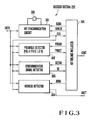
- a conventional radio paging receiver comprises a receiving section 201, a decoder section 202, and an alert generator 203, as shown in Fig. 2.
- the receiving section 201 is intermittently operated in response to a battery saving control signal CONT to reduce power consumption.
- the decoder section 202 processes received data DATA demodulated by the receiving section 201.
- the decoder section 202 detects an address of its own receiver from the received data DATA, it outputs an address detection pulse ADET.
- the alert generator 203 performs an alert operation using a speaker, an LED, and the like in response to the address detection pulse ADET.
- the format of a paging signal consists of a preamble (PA) comprising a repetitive pattern of "1" and "0" signals, and a plurality of batches which follow the preamble, as shown in Fig. 6, as recommended in, e.g, the CCIR (CCIR RPC No. 1, also called a POCSAG code).
- One batch includes one synchronization signal (SC) and eight frames.
- An address signal is sent as a codeword in a predetermined frame.
- the decoder section 202 (Fig. 2) comprises a bit synchronization circuit 301, a preamble detector 302, a synchronization signal detector 303, an address detector 304, and a reception controller 305, as shown in Fig. 3.
- the conventional preamble detector comprises a shift register consisting of D flip-flops 401 to 404, and an AND gate 406, as shown in Fig. 4. More specifically, the preamble detector samples the received data DATA in one phase of a clock CLK extracted by the bit synchronization circuit 301 (Fig. 3) to perform a preamble detection operation.
- the operation of the decoder section 202 (Fig. 2) of the conventional paging receiver will be described below.
- the operation of the decoder section can be classified into three states, i.e., a preamble search mode, a synchronization signal search mode, and an address search mode.
- the bit synchronization circuit 301 corrects the phase of a clock to be synchronous with the received signal.
- the preamble detector 302 samples the received data DATA in response to the clock CLK output from the bit synchronization circuit 301, and checks the presence/absence of the preamble PA.
- the alert generator 203 (Fig. 2) is enabled, to make the speaker, the LED, and the like operate, thus alerting the user to detection of paging.
- the decoder section is restored to the preamble (PA) search mode.
- PA preamble
- SC synchronization signal
- the preamble detector 302 checks the preamble PA in only one phase of the clock output from the bit synchronization circuit 301. Therefore, in the preamble search mode, the decoder section first performs a bit synchronizing operation, and detects a preamble after bit synchronization is established. Therefore, it takes much time until the preamble is detected. In other words, when the receiving section is intermittently operated, the ON time of the receiver (T BS in Fig. 5A) must be increased by a time period necessary for bit synchronization, resulting in poor battery saving efficiency.
- the conventional preamble detector shown in Fig. 4 may fail to receive the preamble of the second data burst when the duty ratio of the preamble is offset from 50% due to an offset of characteristics of the receiving section, as shown in Fig. 7A.
- an address (A3) included in the second burst shown in Fig. 5A cannot often be received.
- a radio paging receiver which comprises a receiving section for intermittently receiving a paging signal including a preamble signal, a synchronization signal, and an address signal, a decoder section for processing a signal demodulated by the receiving section, and an alert generator for generating an alert signal when the decoder section detects an address signal assigned to the receiver, the decoder section including: bit synchronization means for extracting a clock synchronized with a received signal; preamble detection means for detecting the preamble signal and outputting a preamble detection signal; synchronization signal detection means for detecting the synchronization signal and outputting a synchronization signal detection signal; address signal detection means for detecting the address signal assigned to the receiver and outputting an address detection signal; and reception control means responsive to the preamble detection signal and the synchronization signal detection signal for outputting a battery saving control signal controlling an intermittent reception operation of the receiver and a control signal controlling the bit synchronization means, the preamble detection means, the preamble detection means, the pream
- a radio paging receiver according to the present invention has the same arrangement as that shown in Fig. 2, and a decoder section as the principal part of the present invention has substantially the same arrangement as shown in Fig. 3.
- a preamble detector according to the present invention has a quite different arrangement from that of the preamble detector shown in Fig. 3, as will be described later.
- the preamble detector according to this embodiment comprises a first shift register consisting of D flip-flops 101 to 104, a second shift register consisting of D flip-flops 105 to 108, AND gates 110 and 111, and an OR gate 112. More specifically, the preamble detector according to this embodiment has a circuit for sampling received data in a phase different by 180° from a clock CLK extracted by a bit synchronization circuit (Fig. 3) to perform a preamble detection operation in addition to the conventional preamble detector for sampling received data in one phase of the clock CLK extracted by the bit synchronization circuit 301.
- PADET preamble detection pulse
- the operation of the decoder section of the paging receiver according to this embodiment of the present invention will be described below.
- the operation of the decoder section can be classified into three states, i.e., a preamble search mode, a synchronization signal search mode, and an address search mode.
- the ON time (T BS ) of the receiving section 201 can be set to be shorter than the ON time (T BS ′) of the receiving section in the conventional receiver (T BS T BS ′).
- the bit synchronization circuit 301 corrects the phase of the clock CLK to be synchronized with received data DATA.
- the preamble detector 302 samples the received data DATA in two phases of the clock CLK output from the bit synchronization circuit 301 (at the leading and trailing edges of the clock CLK) to check the presence/absence of the preamble.
- SC synchronization signal
- the decoder section is restored to the preamble (PA) search mode.
- PA preamble
- SC synchronization signal
- first and second data bursts are consecutively sent, and have different bit synchronization timings.
- the shift register fetches all "0"s like in the conventional receiver at the leading edge of the clock, and cannot detect the preamble.
- the decoder section enters the synchronization signal search mode. Therefore, as shown in Fig. 5B, correct synchronization can also be established for the second burst. Therefore, an address (A3) included in the second data burst can be reliably detected unlike in the conventional decoder section.
- the preamble detector checks a preamble in a plurality of phases of a clock extracted by the bit synchronization circuit.
- the preamble detector outputs the preamble detection pulse, and can detect the preamble even if bit synchronization is not established.
- battery saving efficiency can be improved, and consecutively input data bursts can be reliably received.
- the preamble detector 302 shown in Fig. 3 is divided into two circuits to check a preamble of received data in a plurality of phases of a clock.
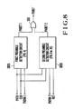
- Fig. 8 shows a preamble detector of the second embodiment.
- the preamble detector shown in Fig. 8 comprises first and second preamble detection circuits 302A and 302B, and an OR gate 350.
- the first preamble detection circuit 302A has the same arrangement as the conventional circuit shown in Fig. 4.
- the second preamble detection circuit 302B is constituted by a circuit shown in Fig. 9.
- reference numerals 501 and 512 denote D flip-flops; 502 and 503, exclusive OR gates; 504 and 505, inverters; 510, an OR gate; 511, an AND gate; and 506 to 509, error counters for counting the number of bits noncoinciding with the preamble.
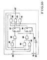
- Each of these error counters 506 to 509 has the arrangement as shown in Fig. 10.
- reference numerals 607 and 608 denote D flip-flops; 605, an exclusive OR gate; 606, an inverter; 602 and 604, OR gates; 601, 603, 609, and 611, AND gates; and 610, a NAND gate.
- Fig. 10 shows a counter for judging whether or not an error count is 2 or less.
- An input terminal ERR receives "1" when there is an error; "0" when there is no error.
- An input terminal RST receives "1" when the error count stored in the flip-flops 607 and 608 is cleared.
- the signals to the terminals ERR and RST are input in synchronism with a clock input from the input terminal CK.
- the flip-flops 607 and 608 store an error count.
- the flip-flop 607 indicates the units digit
- the flip-flop 608 indicates the tens digit.
- the D flip-flop 512 (Fig. 9) generates a Q output corresponding to a preamble pattern (0101%) on the basis of a clock CLK.
- the exclusive OR gate 502 compares received data DATA with the preamble pattern generated by the D flip-flop 512.
- the error counter 506 counts the number of noncoincidences between the received data DATA and the preamble pattern (0101%) from the D flip-flop 512, and outputs a DET pulse when the error count is equal to or smaller than 2.
- the error counter 507 counts the number of noncoincidences between the received data DATA and a pattern (1010%) inverted by the inverter 504, and outputs a DET pulse when the error count is equal to or smaller than 2 like in the error counter 506.
- the D flip-flop 501 fetches the received data DATA at the timing of the clock CLK, and shifts the received data DATA by a half-bit time.
- the exclusive OR gate 503 compares the data shifted by the half-bit time and the preamble pattern (0101). For this reason, the exclusive OR gate 503 makes comparison in a phase shifted by 180° from that of the exclusive OR gate 502.
- the error counters 508 and 509 respectively count the numbers of noncoincidences of the half-bit shifted data with the patterns 0101... and 1010... like in the error counters 506 and 507, and output a DET pulse when the error count is equal to or smaller than 2 like in the error counter 506.
- Fig. 5C shows timing charts of signals output in this embodiment.
- the number of flip-flops constituting the preamble detector can be decreased as compared to the first embodiment shown in Fig. 1.
- the first preamble detection circuit 302A since the first preamble detection circuit 302A has the conventional circuit arrangement, it operates before the synchronization signal SC is detected, as can be seen from Fig. 5C, and the second preamble detection circuit 302B operates after the synchronization signal SC is detected.
- the first preamble detection circuit 302A can check the presence/absence of the preamble for every bit
- the second preamble detection circuit 302B can check the presence/absence of the preamble in units of the number of bits of the address signal.
- Fig. 11 shows an arrangement of the reception controller 305 shown in Fig. 3.
- reference numeral 701 denotes a modulo 32 counter for counting one word, i.e., 32 bits; and 702, a modulo 17 counter for counting one batch, i.e., 17 words.
- Reference numerals 705 and 706 denote S-R flip-flips. These flip-flops 705 and 706 perform an operation for discriminating three operation modes, i.e., the preamble (PA) search mode, the SC search mode, and the address search mode.
- PA preamble
- SC SC search mode
- address search mode the address search mode
- Reference numerals 708 and 709 denote first and second timers.
- the first timer 708 outputs a time-out pulse when the SC cannot be detected within a predetermined period of time in the SC search mode.
- the second timer 709 outputs a time-out pulse when the SC cannot be received within a predetermined period of time.
- Reference numeral 710 denotes a gate circuit.
- the gate circuit 710 outputs various control signals in accordance with outputs M1 and M2 of the flip-flops 705 and 706 and the counts of the modulo 32 counter 701 and the modulo 17 counter 702 associated with the operation mode at timings shown in Figs. 5B and 5C.
- the bit synchronization circuit sets a larger time constant for the clock phase correction after the synchronization signal is detected than that before detection.
- Fig. 12 is a state transition diagram of the three operation modes of the controller. More specifically, in the preamble search mode, the controller enters the SC search mode in response to the PADET pulse, and enters the address search mode in response to the SCDET pulse. In the SC search mode, the controller enters the address search mode in response to the SCDET pulse, and enters the preamble search mode in response to the time-out pulse from the first timer 708. In the address search mode, the controller enters the SC search mode in response to the PADET pulse, and enters the preamble search mode in response to the time-out pulse from the second timer 709.
Landscapes
- Engineering & Computer Science (AREA)
- Computer Networks & Wireless Communication (AREA)
- Signal Processing (AREA)
- Physics & Mathematics (AREA)
- Electromagnetism (AREA)
- General Physics & Mathematics (AREA)
- Synchronisation In Digital Transmission Systems (AREA)
- Mobile Radio Communication Systems (AREA)
Applications Claiming Priority (2)
| Application Number | Priority Date | Filing Date | Title |
|---|---|---|---|
| JP306837/88 | 1988-12-06 | ||
| JP63306837A JP2679185B2 (ja) | 1988-12-06 | 1988-12-06 | 無線選択呼び出し信号受信機 |
Publications (3)
| Publication Number | Publication Date |
|---|---|
| EP0372473A2 true EP0372473A2 (de) | 1990-06-13 |
| EP0372473A3 EP0372473A3 (de) | 1991-12-18 |
| EP0372473B1 EP0372473B1 (de) | 1997-07-09 |
Family
ID=17961854
Family Applications (1)
| Application Number | Title | Priority Date | Filing Date |
|---|---|---|---|
| EP89122380A Expired - Lifetime EP0372473B1 (de) | 1988-12-06 | 1989-12-05 | Funkrufempfänger |
Country Status (7)
| Country | Link |
|---|---|
| EP (1) | EP0372473B1 (de) |
| JP (1) | JP2679185B2 (de) |
| KR (1) | KR920007092B1 (de) |
| AU (1) | AU623710B2 (de) |
| CA (1) | CA2004590C (de) |
| DE (1) | DE68928163T2 (de) |
| HK (1) | HK1001017A1 (de) |
Cited By (1)
| Publication number | Priority date | Publication date | Assignee | Title |
|---|---|---|---|---|
| WO2004049652A1 (en) * | 2002-11-26 | 2004-06-10 | Qualcomm Incorporated | Preamble detection and data rate control in a umts system |
Families Citing this family (2)
| Publication number | Priority date | Publication date | Assignee | Title |
|---|---|---|---|---|
| US6138001A (en) * | 1996-03-12 | 2000-10-24 | Ntt Mobile Communications Network, Inc. | Scheme for intermittent reception of paging signals in mobile communication system |
| JPH11341538A (ja) | 1998-05-29 | 1999-12-10 | Nec Shizuoka Ltd | 無線通信装置 |
Citations (3)
| Publication number | Priority date | Publication date | Assignee | Title |
|---|---|---|---|---|
| WO1981000800A1 (en) * | 1979-09-12 | 1981-03-19 | Gen Electric | Improved binary detecting and threshold circuit |
| GB2144565A (en) * | 1983-08-03 | 1985-03-06 | Multitone Electronics Plc | Decoding arrangements |
| EP0234201A2 (de) * | 1986-01-10 | 1987-09-02 | Nec Corporation | Rufempfänger mit Schaltung zur Batterieschonung |
Family Cites Families (3)
| Publication number | Priority date | Publication date | Assignee | Title |
|---|---|---|---|---|
| JPS6013588B2 (ja) * | 1977-09-16 | 1985-04-08 | 日本電気株式会社 | 無線個別呼出受信機 |
| JPS56136050A (en) * | 1980-03-28 | 1981-10-23 | Nec Corp | Individual selective call reception system |
| GB2136178A (en) * | 1983-02-25 | 1984-09-12 | Philips Electronic Associated | Pager decoding system |
-
1988
- 1988-12-06 JP JP63306837A patent/JP2679185B2/ja not_active Expired - Fee Related
-
1989
- 1989-12-05 EP EP89122380A patent/EP0372473B1/de not_active Expired - Lifetime
- 1989-12-05 AU AU45942/89A patent/AU623710B2/en not_active Ceased
- 1989-12-05 CA CA002004590A patent/CA2004590C/en not_active Expired - Fee Related
- 1989-12-05 DE DE68928163T patent/DE68928163T2/de not_active Expired - Fee Related
- 1989-12-06 KR KR1019890018018A patent/KR920007092B1/ko not_active IP Right Cessation
-
1997
- 1997-12-23 HK HK97102588A patent/HK1001017A1/xx not_active IP Right Cessation
Patent Citations (3)
| Publication number | Priority date | Publication date | Assignee | Title |
|---|---|---|---|---|
| WO1981000800A1 (en) * | 1979-09-12 | 1981-03-19 | Gen Electric | Improved binary detecting and threshold circuit |
| GB2144565A (en) * | 1983-08-03 | 1985-03-06 | Multitone Electronics Plc | Decoding arrangements |
| EP0234201A2 (de) * | 1986-01-10 | 1987-09-02 | Nec Corporation | Rufempfänger mit Schaltung zur Batterieschonung |
Cited By (2)
| Publication number | Priority date | Publication date | Assignee | Title |
|---|---|---|---|---|
| WO2004049652A1 (en) * | 2002-11-26 | 2004-06-10 | Qualcomm Incorporated | Preamble detection and data rate control in a umts system |
| CN100452758C (zh) * | 2002-11-26 | 2009-01-14 | 高通股份有限公司 | 在umts系统中的报头检测和数据速率控制 |
Also Published As
| Publication number | Publication date |
|---|---|
| EP0372473B1 (de) | 1997-07-09 |
| EP0372473A3 (de) | 1991-12-18 |
| HK1001017A1 (en) | 1998-05-15 |
| DE68928163T2 (de) | 1997-12-04 |
| CA2004590C (en) | 1993-10-05 |
| AU4594289A (en) | 1990-06-14 |
| CA2004590A1 (en) | 1990-06-06 |
| JPH02153633A (ja) | 1990-06-13 |
| AU623710B2 (en) | 1992-05-21 |
| JP2679185B2 (ja) | 1997-11-19 |
| DE68928163D1 (de) | 1997-08-14 |
| KR900011171A (ko) | 1990-07-11 |
| KR920007092B1 (ko) | 1992-08-24 |
Similar Documents
| Publication | Publication Date | Title |
|---|---|---|
| EP0071425B1 (de) | Synchronisation eines drahtlosen digitalen Selektivrufempfängers | |
| US4652875A (en) | Pager with improved battery saving function | |
| US4961073A (en) | Battery saving apparatus and method providing optimum synchronization codeword detection | |
| US4837854A (en) | Paging receiver having a noise-immune verification circuit for disabling battery saving operation | |
| JP2646831B2 (ja) | 選択呼出受信機 | |
| US4663623A (en) | Decoding arrangements for synchronous receivers | |
| US6008746A (en) | Method and apparatus for decoding noisy, intermittent data, such as manchester encoded data or the like | |
| JPH0431448B2 (de) | ||
| EP0568856B1 (de) | Pagingreceiver mit Detektion der Daten-Geschwindigkeit zur Fortsetzung des Empfangs der Adressdaten | |
| US5227777A (en) | Radio paging receiver for intermittently receiving a paging signal transmitted on different phases of a clock | |
| JP2630233B2 (ja) | バッテリーセービング機能をもつ無線選択呼出受信機 | |
| US5734686A (en) | Selective power supply control for battery saving effectively | |
| EP0372473A2 (de) | Funkrufempfänger | |
| US5525974A (en) | Radio selective calling receiver for receiving a call signal intermittently under an asynchronous system | |
| JPS6324573B2 (de) | ||
| KR950002441B1 (ko) | 전력소모 절약방식의 페이져 송신신호 수신방법 | |
| JP2000125329A (ja) | 選択呼出受信機 | |
| JPH0629909A (ja) | 選択呼出し受信機における同期確立方法及び装置 | |
| JPH08251645A (ja) | ページャの同期検出装置及び同期検出方法 | |
| JPH0298226A (ja) | 信号検出方式 | |
| JPH04503594A (ja) | バッテリセイビング装置及び最適な同期コードワード検出を提供する方法 |
Legal Events
| Date | Code | Title | Description |
|---|---|---|---|
| PUAI | Public reference made under article 153(3) epc to a published international application that has entered the european phase |
Free format text: ORIGINAL CODE: 0009012 |
|
| 17P | Request for examination filed |
Effective date: 19900103 |
|
| AK | Designated contracting states |
Kind code of ref document: A2 Designated state(s): DE GB NL SE |
|
| PUAL | Search report despatched |
Free format text: ORIGINAL CODE: 0009013 |
|
| AK | Designated contracting states |
Kind code of ref document: A3 Designated state(s): DE GB NL SE |
|
| 17Q | First examination report despatched |
Effective date: 19940228 |
|
| GRAG | Despatch of communication of intention to grant |
Free format text: ORIGINAL CODE: EPIDOS AGRA |
|
| GRAH | Despatch of communication of intention to grant a patent |
Free format text: ORIGINAL CODE: EPIDOS IGRA |
|
| GRAH | Despatch of communication of intention to grant a patent |
Free format text: ORIGINAL CODE: EPIDOS IGRA |
|
| GRAA | (expected) grant |
Free format text: ORIGINAL CODE: 0009210 |
|
| STAA | Information on the status of an ep patent application or granted ep patent |
Free format text: STATUS: THE PATENT HAS BEEN GRANTED |
|
| AK | Designated contracting states |
Kind code of ref document: B1 Designated state(s): DE GB NL SE |
|
| REF | Corresponds to: |
Ref document number: 68928163 Country of ref document: DE Date of ref document: 19970814 |
|
| PLBE | No opposition filed within time limit |
Free format text: ORIGINAL CODE: 0009261 |
|
| 26N | No opposition filed | ||
| PGFP | Annual fee paid to national office [announced via postgrant information from national office to epo] |
Ref country code: NL Payment date: 20001231 Year of fee payment: 12 |
|
| REG | Reference to a national code |
Ref country code: GB Ref legal event code: IF02 |
|
| PG25 | Lapsed in a contracting state [announced via postgrant information from national office to epo] |
Ref country code: NL Free format text: LAPSE BECAUSE OF NON-PAYMENT OF DUE FEES Effective date: 20020701 |
|
| NLV4 | Nl: lapsed or anulled due to non-payment of the annual fee |
Effective date: 20020701 |
|
| PGFP | Annual fee paid to national office [announced via postgrant information from national office to epo] |
Ref country code: SE Payment date: 20031204 Year of fee payment: 15 |
|
| PG25 | Lapsed in a contracting state [announced via postgrant information from national office to epo] |
Ref country code: SE Free format text: LAPSE BECAUSE OF NON-PAYMENT OF DUE FEES Effective date: 20041206 |
|
| EUG | Se: european patent has lapsed | ||
| PGFP | Annual fee paid to national office [announced via postgrant information from national office to epo] |
Ref country code: GB Payment date: 20071205 Year of fee payment: 19 |
|
| PGFP | Annual fee paid to national office [announced via postgrant information from national office to epo] |
Ref country code: DE Payment date: 20071129 Year of fee payment: 19 |
|
| GBPC | Gb: european patent ceased through non-payment of renewal fee |
Effective date: 20081205 |
|
| PG25 | Lapsed in a contracting state [announced via postgrant information from national office to epo] |
Ref country code: DE Free format text: LAPSE BECAUSE OF NON-PAYMENT OF DUE FEES Effective date: 20090701 |
|
| PG25 | Lapsed in a contracting state [announced via postgrant information from national office to epo] |
Ref country code: GB Free format text: LAPSE BECAUSE OF NON-PAYMENT OF DUE FEES Effective date: 20081205 |