EP0371663B1 - Tampon de sortie de circuit intégré ayant une protection esd modifiée - Google Patents
Tampon de sortie de circuit intégré ayant une protection esd modifiée Download PDFInfo
- Publication number
- EP0371663B1 EP0371663B1 EP89311910A EP89311910A EP0371663B1 EP 0371663 B1 EP0371663 B1 EP 0371663B1 EP 89311910 A EP89311910 A EP 89311910A EP 89311910 A EP89311910 A EP 89311910A EP 0371663 B1 EP0371663 B1 EP 0371663B1
- Authority
- EP
- European Patent Office
- Prior art keywords
- bondpad
- resistor
- integrated circuit
- output buffer
- output
- Prior art date
- Legal status (The legal status is an assumption and is not a legal conclusion. Google has not performed a legal analysis and makes no representation as to the accuracy of the status listed.)
- Expired - Lifetime
Links
- 239000000872 buffer Substances 0.000 title claims description 48
- 239000004020 conductor Substances 0.000 claims description 22
- 229910052751 metal Inorganic materials 0.000 claims description 21
- 239000002184 metal Substances 0.000 claims description 21
- 229910021332 silicide Inorganic materials 0.000 claims description 19
- FVBUAEGBCNSCDD-UHFFFAOYSA-N silicide(4-) Chemical compound [Si-4] FVBUAEGBCNSCDD-UHFFFAOYSA-N 0.000 claims description 19
- 229910021420 polycrystalline silicon Inorganic materials 0.000 claims description 9
- 229920005591 polysilicon Polymers 0.000 claims description 8
- 238000000034 method Methods 0.000 description 10
- 230000001681 protective effect Effects 0.000 description 9
- 238000012360 testing method Methods 0.000 description 8
- 238000013461 design Methods 0.000 description 7
- 239000000758 substrate Substances 0.000 description 6
- 229910052782 aluminium Inorganic materials 0.000 description 5
- XAGFODPZIPBFFR-UHFFFAOYSA-N aluminium Chemical compound [Al] XAGFODPZIPBFFR-UHFFFAOYSA-N 0.000 description 5
- 239000004065 semiconductor Substances 0.000 description 5
- VYPSYNLAJGMNEJ-UHFFFAOYSA-N Silicium dioxide Chemical compound O=[Si]=O VYPSYNLAJGMNEJ-UHFFFAOYSA-N 0.000 description 4
- 238000005516 engineering process Methods 0.000 description 4
- 229910021341 titanium silicide Inorganic materials 0.000 description 3
- 229910052581 Si3N4 Inorganic materials 0.000 description 2
- WYTGDNHDOZPMIW-RCBQFDQVSA-N alstonine Natural products C1=CC2=C3C=CC=CC3=NC2=C2N1C[C@H]1[C@H](C)OC=C(C(=O)OC)[C@H]1C2 WYTGDNHDOZPMIW-RCBQFDQVSA-N 0.000 description 2
- 230000000694 effects Effects 0.000 description 2
- 239000000463 material Substances 0.000 description 2
- 235000012239 silicon dioxide Nutrition 0.000 description 2
- 239000000377 silicon dioxide Substances 0.000 description 2
- HQVNEWCFYHHQES-UHFFFAOYSA-N silicon nitride Chemical compound N12[Si]34N5[Si]62N3[Si]51N64 HQVNEWCFYHHQES-UHFFFAOYSA-N 0.000 description 2
- 238000010420 art technique Methods 0.000 description 1
- 230000009286 beneficial effect Effects 0.000 description 1
- YXTPWUNVHCYOSP-UHFFFAOYSA-N bis($l^{2}-silanylidene)molybdenum Chemical compound [Si]=[Mo]=[Si] YXTPWUNVHCYOSP-UHFFFAOYSA-N 0.000 description 1
- 239000003990 capacitor Substances 0.000 description 1
- 239000000969 carrier Substances 0.000 description 1
- 230000015556 catabolic process Effects 0.000 description 1
- 239000001679 citrus red 2 Substances 0.000 description 1
- 239000010941 cobalt Substances 0.000 description 1
- 229910017052 cobalt Inorganic materials 0.000 description 1
- GUTLYIVDDKVIGB-UHFFFAOYSA-N cobalt atom Chemical compound [Co] GUTLYIVDDKVIGB-UHFFFAOYSA-N 0.000 description 1
- 238000007599 discharging Methods 0.000 description 1
- 230000005669 field effect Effects 0.000 description 1
- 238000002347 injection Methods 0.000 description 1
- 239000007924 injection Substances 0.000 description 1
- 239000012212 insulator Substances 0.000 description 1
- 238000004519 manufacturing process Methods 0.000 description 1
- 229910021344 molybdenum silicide Inorganic materials 0.000 description 1
- 238000012545 processing Methods 0.000 description 1
- 238000012358 sourcing Methods 0.000 description 1
- 229910052715 tantalum Inorganic materials 0.000 description 1
- GUVRBAGPIYLISA-UHFFFAOYSA-N tantalum atom Chemical compound [Ta] GUVRBAGPIYLISA-UHFFFAOYSA-N 0.000 description 1
- 238000012956 testing procedure Methods 0.000 description 1
Images


Classifications
-
- H—ELECTRICITY
- H10—SEMICONDUCTOR DEVICES; ELECTRIC SOLID-STATE DEVICES NOT OTHERWISE PROVIDED FOR
- H10D—INORGANIC ELECTRIC SEMICONDUCTOR DEVICES
- H10D89/00—Aspects of integrated devices not covered by groups H10D84/00 - H10D88/00
- H10D89/60—Integrated devices comprising arrangements for electrical or thermal protection, e.g. protection circuits against electrostatic discharge [ESD]
- H10D89/601—Integrated devices comprising arrangements for electrical or thermal protection, e.g. protection circuits against electrostatic discharge [ESD] for devices having insulated gate electrodes, e.g. for IGFETs or IGBTs
Definitions
- This invention relates to integrated circuit output buffers.
- ESD electrostatic discharge
- IC integrated circuit
- the input and output buffer stages are susceptible to damage, since they connect directly to the package terminals. That is, an over-voltage condition on the package terminals, as due to an ESD event, can easily damage circuitry that is designed for operation at low voltage, typically 5 volts or less.
- ESD typically causes damage to the gate oxides of input buffers, whereas for output circuitry, damage to the drain regions often results. Still other forms of damage are possible.
- over-voltage clamping devices typically diodes or transistors. These devices are typically connected between an input/output bondpad and a power supply conductor. In one design, the clamping device is located around the periphery of the bondpad; see U.S. patent 4,806,999 and U.S. patent 4,821,089 co-assigned with the present invention.
- various combinations of clamping diodes, transistors, and resistors are used between the input bondpad and the input transistors to limit the voltage that appears at the input gates.
- protective clamping diodes have also been used for the protection of output buffers, these have not provided as high an amount of protection as desired in many cases.
- a resistor is included between the drain of the n-channel transistor in a given buffer and the corresponding bondpad.
- multiple n-channel output transistor drain regions are each connected to the bondpad through a separate resistor.
- the resistors are desirably formed in a deposited layer, typically doped polysilicon or metal silicide, overlying the semiconductor substrate.
- the bondpad is also connected to over-voltage clamping means, typically one or more diodes or transistors.
- the present invention relates to an integrated circuit having improved protection against electrostatic discharge (ESD).
- ESD electrostatic discharge
- the inventive technique affords a significant improvement as measured by the "human body model”, discussed below, even for silicided output buffers that are the most susceptible to breakdown.
- the present technique has a minimal effect on the performance of the protected output buffer, and may be implemented in CMOS technology without additional processing steps.
- an output buffer in CMOS technology comprises p-channel transistor 11 and n-channel transistor 12 having their drains connected to a common buffer output node 13.
- a silicide resistor 14 is connected between the node 13 and the output bondpad 17.
- voltage clamping diodes 15 and 16 are connected to the bondpad and to the power supply conductors V DD and V SS accordingly. As discussed below, the diodes 15 and 16 may be disposed around the periphery of the bondpad to minimize resistance and inductance, thereby ensuring fast clamping action for maximum protection.
- resistor 14 in this arrangement may be very low, allowing good performance, while still achieving a significant improvement in ESD protection on the human body model test, discussed below.
- the value of this resistor is in the range of 2 to 10 ohms, although a higher value is suitable in the case of a relatively small output buffer driving a small load. I estimate that a value up to about 20 ohms is useful for small output buffers, whereas a value as low as 1 ohm still provides useful protection, while allowing for high performance from a relatively large output buffer.
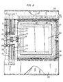
- FIG. 2 a top view of a typical layout of the buffer of Fig. 1 is shown.
- An output bondpad typically aluminum, has a central portion 200 that is used for wire bonding to a package terminal.
- the periphery 213 of the bondpad is covered with an insulator, typically being a portion of a silicon dioxide or silicon nitride "cap" layer.
- the top half (as viewed) of the periphery of the bondpad extends down through contact windows 201 to a p-type semiconductor region 215, which forms the anode of diode 15.
- the underlying n-type semiconductor region (typically a n-tub) forms the cathode of diode 15, and is connected through contact windows to the positive power supply voltage (V DD ) conductor 203.
- the bottom half of the bondpad is connected through contact windows 202 to the n-type cathode region 216 of diode 16.
- the underling p-type anode region of diode 16 (typically a p-tub) is connected through contact windows to the negative power supply voltage (V SS ) conductor 204.
- V SS negative power supply voltage
- the metal silicide link 205 connects the bondpad to the output buffer, and provides the required resistance for proper ESD protection.
- a link of titanium silicide having a thickness of 100 nanometers (1000 angstroms), a width of 10 micrometers, and a length of 20 micrometers provides a resistance of about 3 ohms.
- Other geometries may readily be determined that obtain the desired resistance, based upon the resistivity of the silicide employed, which is about 1.5 ohms per square in the case of titanium silicide.
- the bondpad is connected to one side of the silicide resistor through contact windows 214.
- the drains of the p and n channel output transistors underlie metal contact regions 207 and 208, respectively, which contact the other side of the resistor through contact windows 206.
- Regions 209 and 210 are the gate electrodes, and regions 211 and 212 are the metal contacts to the sources of the p and n channel output transistors, respectively.
- the p-channel transistor is surrounded by an optional guard ring, comprising a metal layer 217 connected to V DD , which contacts a n-type ring located thereunder.
- the n-channel transistor is surrounded by an optional guard ring comprising metal layer 218 connected to V SS , which contacts a p-type ring thereunder.
- FIGS. 1 and 2 In order to distinguish the case wherein a metal silicide interconnect has been used in the prior art between the output buffer and the bondpad for layout reasons, the embodiment of FIGS. 1 and 2 is described in terms of integrated circuits having two (or more) metal interconnect levels.
- the central portion of the metal bondpad 200 includes both the first and second metal layers.
- the V DD and V SS busses 203 and 204 are formed from both the first and the second metal layer, whereas the source/drain contacts 207, 208, 211, 212 are formed from only the first level metal layer.
- the protective resistor 14 is connected between the output node 13 and the bondpad 17. This provides for a convenient layout for the buffer circuitry. However, it is alternately possible to connect the protective resistor between the drain of the n-channel transistor 12 and the output node 13. This results in the connection of the protective resistor as shown as 14' in the embodiment of the invention shown in Fig. 3. This still results in a substantial improvement in ESD performance, since the n-channel transistor in practice is more susceptible to ESD damage than the p-channel transistor 11. Furthermore, it allows the p-channel device, which typically tends to have a lower performance than the n-channel device, to be connected directly to the bondpad. Note that it does not appear that the connection of Fig. 3 has been required in the prior art for layout purposes with either single level or multi-level interconnect techniques. Note also that in either case, the protective resistor is in the path between the drain of the n-channel transistor 12 and the bondpad 17.
- a silicided resistor has been shown in the illustrative embodiment herein, which is compatible with the "salicide" technique for forming silicided source, drain, and gate electrodes. It is of course very advantageous to be able to solve the ESD problem in such structures, which are more susceptible to ESD than other designs. Furthermore, the salicide technique is becoming increasingly common with integrated circuits at the sub-micron level. However, the present invention is not limited to the use of silicided resistors, or with the salicide technique. For example, a doped polysilicon resistor may be used to provide the resistance in the desired range. Furthermore, it is well known to form transistors having silicided gate regions, but which do not include a silicide layer on the source/drain regions. Such transistors also obtain improved ESD protection by the use of the inventive technique.
- a presently preferred embodiment of the invention utilizes multiple resistors.
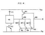
- This is illustrated in Fig. 4, which shows a CMOS output buffer protected in this manner.
- This buffer comprises a p-channel pull-up transistor 401 and multiple (e.g., 3) n-channel pull-down transistors 403, 404 and 405.
- transistors 403, 404 and 405 typically are constructed using a common gate electrode, and may be considered a single pull-down device having multiple drain (and source) regions. This is often used in prior art designs in order to increase the output drive capability of the buffer.
- transistor 401 is shown as a single device, it may also comprise multiple source and drain regions for increased drive capability, as in prior art designs.
- the gates of the transistors are coupled to an input node 400, which receives the buffer input signal.
- resistors 406, 407, and 408 These resistors connect the drains of the n-channel pull-down device to the output node 409, which is connected to the bondpad 410. I have found that the use of multiple resistors aids in reducing the likelihood of damage from ESD events, allowing for higher test voltage ratings according to standard ESD testing procedures.
- the resistors typically each have a value in the range of 1 to 100 ohms, and more typically in the range of 5 to 50 ohms.
- the resistors are formed in a conductive layer overlying, and insulated from, the substrate.
- the resistors may be conveniently implemented using a doped polysilicon or metal silicide conductor layer. They may be formed in the same layer used to form the gate electrodes, if desired.
- resistors may also be formed by doped regions in the semiconductor substrate.
- n+ regions formed in a p-tub could be envisioned as resistors.
- forming the resistors in a deposited conductive layer overlying, and insulated from, the substrate e.g., a polysilicon or silicide layer
- resistors are formed directly in a tub region, for example a n-tub.
- resistors formed in a deposited conductor provides for a more compact design. This is due in part to the spacing requirements for preventing "short channel" effects when a n-tub resistor is used. Therefore, the presently preferred embodiment utilizes multiple resistors formed in a deposited conductor layer.
- the resistors typically have a resistance of at least 1 ohm, in order to obtain enhanced ESD protection.
- over-voltage clamping devices connected to the bondpad. These may be diodes, transistors, or a combination, and serve to limit the voltage swings that are in excess of normal operaring voltages. For example, in Fig. 4 diode 411 provides protection from high positive voltages at the bondpad. Similarly, transistor 412 protects from high negative voltages. Note that these devices conduct to the V DD and V SS power supply voltage conductors, respectively. Even though these conductors are not connected to power supply voltages when the integrated circuit is not connected in a circuit (e.g., as during manufacture or shipping), they provide access to a large substrate capacitance and resistance that helps dissipate the ESD energy.
- a physical layout of an illustrative integrated circuit output buffer and its associated bondpad is shown.
- the metallic bondpad 500 typically aluminum
- a dielectric region 501 typically deposited silicon dioxide or silicon nitride.
- the central portion of the bondpad is left free of the dielectric, allowing for a wire bond connection to a package terminal.
- a negative over-voltage clamping device implementing bipolar transistor 412 in Fig. 4.
- This transistor comprises a n+ emitter region 521, a n+ collector region 522, and a p-type base region 523.
- the base region is a portion of the p-tub in which the transistor is formed, with the p-tub being connected to the V SS power supply conductor by means of p+ tub tie contact region 524.
- This bipolar device serves to limit negative voltage swings to about 0.5 volts with respect to the V SS conductor.
- other protective devices e.g., a diode or metal gate field effect transistor
- a protective diode comprising p+ anode region 525, which is formed in a n-tub region 526, which serves as the cathode.
- the n-tub region 526 is connected to the V DD power supply conductor by means of n+ tub tie contact region 527. This diode serves to limit the positive voltage swings to about 0.5 volts positive with respect to the V DD conductor.
- the n-channel output device comprises a serpentine gate electrode 502 which extends between multiple source regions 503 ... 506 and multiple drain regions 507 ... 509. Note that the source and drain regions are overlaid by triangular metal electrodes. Each drain region is connected to the bondpad through a resistor, being regions 510 ... 512. In the illustrative embodiment, the resistors are physically connected directly to the bondpad around its edge. However, they may alternately be connected to a conductor that connects to the bondpad. In the illustrative case, the resistors are tantalum silicide formed on top of doped polycrystalline silicon, and have a sheet resistivity of 2.5 ohms per square.
- resistor materials e.g., doped polysilicon, molybdenum silicide, titanium silicide, cobalt silicide, etc.
- the resistor geometry may be chosen as needed to obtain the desired resistance.
- silicide resistors may be formed during the "salicide” process that forms the silicide on gate, source, and drain regions.
- the p-channel pull-up transistor comprising serpentine gate electrode 513, multiple source regions 514 ... 517 and multiple drain regions 518 ... 520. As can be seen, the drain regions are connected by means of aluminum conductors directly to the bondpad.
- the present technique has been used with output buffers on an IC chip implemented in 1.25 micrometer CMOS technology.
- the buffers were found to have ESD protection typically in excess of 2500 volts, as measured by the "human body model" test. This is an industry standard test that involves discharging a 100 picofarad capacitor through a 1500 ohm resistor into the output pin connected to the bondpad. In these tests, the V SS or V DD pins were grounded, while the other pins were left floating. In addition to this test, the latch-up resistance of the chip was found to be at a suitably high level.
- any number may be employed, depending on the design of the output buffer.
- output buffers requiring higher current drive capabilities utilize a greater number of drain regions, and hence a greater number of resistors.
- 17 drain regions are used.
- two voltage clamping devices are typically used (one for each polarity), that is not necessary in all cases.
- the p+/n-tub diode regions 525 ... 527) may be omitted, because the junction formed by the p+ drain and n-tub will provide for the positive clamping action. Still other variations will be apparent to a person of skill in the art.
- CMOS complementary metal-oxide-semiconductor
- inventive technique may be used to protect integrated circuits formed with III-V semiconductor materials as well.
Landscapes
- Metal-Oxide And Bipolar Metal-Oxide Semiconductor Integrated Circuits (AREA)
- Semiconductor Integrated Circuits (AREA)
- Elimination Of Static Electricity (AREA)
- Logic Circuits (AREA)
- Electronic Switches (AREA)
Claims (4)
- Circuit intégré comprenant un tampon de sortie ayant un transistor d'excursion haute à canal p (11) et un transistor d'excursion basse à canal n (12) dont les drains sont couplés à une plage de connexion commune (17) qui est connectée à un conducteur externe, et un moyen de fixation de niveau de tension (15,16) connecté à ladite plage de connexion, CARACTERISE PAR une résistance (14') ayant une résistance supérieure à 1 ohm et inférieure à 20 ohms connectée entre le drain dudit transistor à canal n et ladite plage de connexion, dans lequel ladite résistance est une résistance en polysilicium ou siliciure dopé, et le drain dudit transistor à canal p est connecté directement à ladite plage de connexion.
- Circuit intégré selon la revendication 1, dans lequel lesdits transistors ont des électrodes de grille, source et drain siliciées, et ladite résistance est une résistance siliciée.
- Circuit intégré selon la revendication 1 ou 2, dans lequel ledit moyen de fixation de niveau de tension est une paire de diodes, la première diode de ladite paire a une région d'anode de type p connectée à ladite plage de connexion et une région de cathode de type n connectée à un conducteur de tension d'alimentation positif, et la seconde diode de ladite paire a une région de cathode de type n connectée à ladite plage de connexion et une région d'anode de type p connectée à un conducteur de tension d'alimentation négatif.
- Circuit intégré selon l'une quelconque des revendications précédentes comprenant au moins deux niveaux de conducteurs métalliques.
Applications Claiming Priority (4)
| Application Number | Priority Date | Filing Date | Title |
|---|---|---|---|
| US27504888A | 1988-11-22 | 1988-11-22 | |
| US275048 | 1988-11-22 | ||
| US41609989A | 1989-10-02 | 1989-10-02 | |
| US416099 | 1989-10-02 |
Publications (2)
| Publication Number | Publication Date |
|---|---|
| EP0371663A1 EP0371663A1 (fr) | 1990-06-06 |
| EP0371663B1 true EP0371663B1 (fr) | 1994-06-15 |
Family
ID=26957227
Family Applications (1)
| Application Number | Title | Priority Date | Filing Date |
|---|---|---|---|
| EP89311910A Expired - Lifetime EP0371663B1 (fr) | 1988-11-22 | 1989-11-16 | Tampon de sortie de circuit intégré ayant une protection esd modifiée |
Country Status (5)
| Country | Link |
|---|---|
| EP (1) | EP0371663B1 (fr) |
| JP (1) | JPH0831531B2 (fr) |
| DE (1) | DE68916192T2 (fr) |
| ES (1) | ES2055795T3 (fr) |
| HK (1) | HK137095A (fr) |
Cited By (2)
| Publication number | Priority date | Publication date | Assignee | Title |
|---|---|---|---|---|
| DE19844145A1 (de) * | 1998-09-25 | 2000-01-05 | Siemens Ag | Kapazitätslade- und Entladeschaltung mit Überspannungsschutz |
| US7227730B2 (en) | 2004-05-28 | 2007-06-05 | Infineon Technolgoies Ag | Device for ESD protection of an integrated circuit |
Families Citing this family (10)
| Publication number | Priority date | Publication date | Assignee | Title |
|---|---|---|---|---|
| EP0517391A1 (fr) * | 1991-06-05 | 1992-12-09 | STMicroelectronics, Inc. | Circuit de protection ESD |
| JP2997858B2 (ja) * | 1992-11-09 | 2000-01-11 | 三菱電機株式会社 | 半導体集積回路 |
| DE4341170C2 (de) * | 1993-12-02 | 2001-05-03 | Siemens Ag | ESD-Schutzstruktur für integrierte Schaltungen |
| JP2638537B2 (ja) * | 1995-01-11 | 1997-08-06 | 日本電気株式会社 | 半導体装置 |
| SE9900439D0 (sv) | 1999-02-09 | 1999-02-09 | Ericsson Telefon Ab L M | Electrostatic discharge protection of integrated circuits |
| SE522909C2 (sv) | 2001-09-06 | 2004-03-16 | Ericsson Telefon Ab L M | Anordning för skydd av integrerad högfrekvenskrets innefattande en halvledarvaristor |
| SE0302296D0 (sv) | 2003-08-27 | 2003-08-27 | Infineon Technologies Ag | Device for ESD protection of an integrated circuit |
| US8218277B2 (en) * | 2009-09-08 | 2012-07-10 | Xilinx, Inc. | Shared electrostatic discharge protection for integrated circuit output drivers |
| JP5431379B2 (ja) * | 2011-02-03 | 2014-03-05 | シャープ株式会社 | ダイオード保護回路、lnb、およびアンテナシステム |
| US8717723B2 (en) * | 2012-01-10 | 2014-05-06 | Xilinx, Inc. | Driver circuit and method of generating an output signal |
Family Cites Families (4)
| Publication number | Priority date | Publication date | Assignee | Title |
|---|---|---|---|---|
| NL176322C (nl) * | 1976-02-24 | 1985-03-18 | Philips Nv | Halfgeleiderinrichting met beveiligingsschakeling. |
| JPS577966A (en) * | 1980-06-19 | 1982-01-16 | Oki Electric Ind Co Ltd | Semiconductor integrated circuit device |
| JPS6269660A (ja) * | 1985-09-24 | 1987-03-30 | Toshiba Corp | 静電保護回路 |
| JPS6331157A (ja) * | 1986-07-24 | 1988-02-09 | Fujitsu Ltd | C−mos lsiの保護回路 |
-
1989
- 1989-11-16 ES ES89311910T patent/ES2055795T3/es not_active Expired - Lifetime
- 1989-11-16 EP EP89311910A patent/EP0371663B1/fr not_active Expired - Lifetime
- 1989-11-16 DE DE68916192T patent/DE68916192T2/de not_active Expired - Fee Related
- 1989-11-20 JP JP1299917A patent/JPH0831531B2/ja not_active Expired - Lifetime
-
1995
- 1995-08-31 HK HK137095A patent/HK137095A/en not_active IP Right Cessation
Cited By (2)
| Publication number | Priority date | Publication date | Assignee | Title |
|---|---|---|---|---|
| DE19844145A1 (de) * | 1998-09-25 | 2000-01-05 | Siemens Ag | Kapazitätslade- und Entladeschaltung mit Überspannungsschutz |
| US7227730B2 (en) | 2004-05-28 | 2007-06-05 | Infineon Technolgoies Ag | Device for ESD protection of an integrated circuit |
Also Published As
| Publication number | Publication date |
|---|---|
| JPH0831531B2 (ja) | 1996-03-27 |
| ES2055795T3 (es) | 1994-09-01 |
| HK137095A (en) | 1995-09-08 |
| EP0371663A1 (fr) | 1990-06-06 |
| DE68916192T2 (de) | 1994-09-22 |
| JPH02158166A (ja) | 1990-06-18 |
| DE68916192D1 (de) | 1994-07-21 |
Similar Documents
| Publication | Publication Date | Title |
|---|---|---|
| US4990802A (en) | ESD protection for output buffers | |
| US5218222A (en) | Output ESD protection circuit | |
| US5682047A (en) | Input-output (I/O) structure with capacitively triggered thyristor for electrostatic discharge (ESD) protection | |
| US5060037A (en) | Output buffer with enhanced electrostatic discharge protection | |
| US5905288A (en) | Output ESD protection with high-current-triggered lateral SCR | |
| US5270565A (en) | Electro-static discharge protection circuit with bimodal resistance characteristics | |
| US5465189A (en) | Low voltage triggering semiconductor controlled rectifiers | |
| US4996626A (en) | Resistorless electrostatic discharge protection device for high speed integrated circuits | |
| US5043782A (en) | Low voltage triggered snap-back device | |
| US5051860A (en) | Electro-static discharge protection circuit with bimodal resistance characteristics | |
| US6424013B1 (en) | Body-triggered ESD protection circuit | |
| US5701024A (en) | Electrostatic discharge (ESD) protection structure for high voltage pins | |
| US7723792B1 (en) | Floating diodes | |
| EP0242383B1 (fr) | Protection de circuits integres igfet contre les decharges electrostatiques | |
| US4609931A (en) | Input protection MOS semiconductor device with zener breakdown mechanism | |
| EP0371663B1 (fr) | Tampon de sortie de circuit intégré ayant une protection esd modifiée | |
| US6137338A (en) | Low resistance input protection circuit | |
| US9019670B2 (en) | Bi-directional ESD protection circuit | |
| KR100325190B1 (ko) | 반도체집적회로 | |
| US6934136B2 (en) | ESD protection of noise decoupling capacitors | |
| EP0472654B1 (fr) | Dispositif de retour a zero declenche par de faibles tensions | |
| US5514893A (en) | Semiconductor device for protecting an internal circuit from electrostatic damage | |
| US6456474B2 (en) | Semiconductor integrated circuit | |
| US5365103A (en) | Punchthru ESD device along centerline of power pad | |
| US6894881B1 (en) | ESD protection methods and devices using additional terminal in the diode structures |
Legal Events
| Date | Code | Title | Description |
|---|---|---|---|
| PUAI | Public reference made under article 153(3) epc to a published international application that has entered the european phase |
Free format text: ORIGINAL CODE: 0009012 |
|
| AK | Designated contracting states |
Kind code of ref document: A1 Designated state(s): DE ES FR GB IT NL |
|
| 17P | Request for examination filed |
Effective date: 19901128 |
|
| 17Q | First examination report despatched |
Effective date: 19921016 |
|
| GRAA | (expected) grant |
Free format text: ORIGINAL CODE: 0009210 |
|
| AK | Designated contracting states |
Kind code of ref document: B1 Designated state(s): DE ES FR GB IT NL |
|
| ITF | It: translation for a ep patent filed | ||
| RAP4 | Party data changed (patent owner data changed or rights of a patent transferred) |
Owner name: AT&T CORP. |
|
| ET | Fr: translation filed | ||
| REF | Corresponds to: |
Ref document number: 68916192 Country of ref document: DE Date of ref document: 19940721 |
|
| REG | Reference to a national code |
Ref country code: ES Ref legal event code: FG2A Ref document number: 2055795 Country of ref document: ES Kind code of ref document: T3 |
|
| PLBE | No opposition filed within time limit |
Free format text: ORIGINAL CODE: 0009261 |
|
| STAA | Information on the status of an ep patent application or granted ep patent |
Free format text: STATUS: NO OPPOSITION FILED WITHIN TIME LIMIT |
|
| NLT1 | Nl: modifications of names registered in virtue of documents presented to the patent office pursuant to art. 16 a, paragraph 1 |
Owner name: AT&T CORP. TE NEW YORK, NEW YORK, VER. ST. V. AM. |
|
| 26N | No opposition filed | ||
| PGFP | Annual fee paid to national office [announced via postgrant information from national office to epo] |
Ref country code: ES Payment date: 19981106 Year of fee payment: 10 |
|
| PG25 | Lapsed in a contracting state [announced via postgrant information from national office to epo] |
Ref country code: ES Free format text: LAPSE BECAUSE OF NON-PAYMENT OF DUE FEES Effective date: 19991117 |
|
| PGFP | Annual fee paid to national office [announced via postgrant information from national office to epo] |
Ref country code: FR Payment date: 20011022 Year of fee payment: 13 |
|
| PGFP | Annual fee paid to national office [announced via postgrant information from national office to epo] |
Ref country code: NL Payment date: 20011026 Year of fee payment: 13 |
|
| PGFP | Annual fee paid to national office [announced via postgrant information from national office to epo] |
Ref country code: GB Payment date: 20011116 Year of fee payment: 13 |
|
| PGFP | Annual fee paid to national office [announced via postgrant information from national office to epo] |
Ref country code: DE Payment date: 20011230 Year of fee payment: 13 |
|
| REG | Reference to a national code |
Ref country code: GB Ref legal event code: IF02 |
|
| PG25 | Lapsed in a contracting state [announced via postgrant information from national office to epo] |
Ref country code: GB Free format text: LAPSE BECAUSE OF NON-PAYMENT OF DUE FEES Effective date: 20021116 |
|
| PG25 | Lapsed in a contracting state [announced via postgrant information from national office to epo] |
Ref country code: NL Free format text: LAPSE BECAUSE OF NON-PAYMENT OF DUE FEES Effective date: 20030601 |
|
| PG25 | Lapsed in a contracting state [announced via postgrant information from national office to epo] |
Ref country code: DE Free format text: LAPSE BECAUSE OF NON-PAYMENT OF DUE FEES Effective date: 20030603 |
|
| GBPC | Gb: european patent ceased through non-payment of renewal fee | ||
| PG25 | Lapsed in a contracting state [announced via postgrant information from national office to epo] |
Ref country code: FR Free format text: LAPSE BECAUSE OF NON-PAYMENT OF DUE FEES Effective date: 20030731 |
|
| NLV4 | Nl: lapsed or anulled due to non-payment of the annual fee |
Effective date: 20030601 |
|
| REG | Reference to a national code |
Ref country code: FR Ref legal event code: ST |
|
| REG | Reference to a national code |
Ref country code: ES Ref legal event code: FD2A Effective date: 20001214 |
|
| PG25 | Lapsed in a contracting state [announced via postgrant information from national office to epo] |
Ref country code: IT Free format text: LAPSE BECAUSE OF NON-PAYMENT OF DUE FEES;WARNING: LAPSES OF ITALIAN PATENTS WITH EFFECTIVE DATE BEFORE 2007 MAY HAVE OCCURRED AT ANY TIME BEFORE 2007. THE CORRECT EFFECTIVE DATE MAY BE DIFFERENT FROM THE ONE RECORDED. Effective date: 20051116 |