EP0367630B1 - Packung für elektronische Anordnungen zum Betrieb bei verschiedenen jeweiligen Temperaturen - Google Patents
Packung für elektronische Anordnungen zum Betrieb bei verschiedenen jeweiligen Temperaturen Download PDFInfo
- Publication number
- EP0367630B1 EP0367630B1 EP89311436A EP89311436A EP0367630B1 EP 0367630 B1 EP0367630 B1 EP 0367630B1 EP 89311436 A EP89311436 A EP 89311436A EP 89311436 A EP89311436 A EP 89311436A EP 0367630 B1 EP0367630 B1 EP 0367630B1
- Authority
- EP
- European Patent Office
- Prior art keywords
- heat insulating
- insulating vacuum
- vacuum vessel
- substrate
- package
- Prior art date
- Legal status (The legal status is an assumption and is not a legal conclusion. Google has not performed a legal analysis and makes no representation as to the accuracy of the status listed.)
- Expired - Lifetime
Links
Images


Classifications
-
- H—ELECTRICITY
- H01—ELECTRIC ELEMENTS
- H01L—SEMICONDUCTOR DEVICES NOT COVERED BY CLASS H10
- H01L23/00—Details of semiconductor or other solid state devices
- H01L23/34—Arrangements for cooling, heating, ventilating or temperature compensation ; Temperature sensing arrangements
- H01L23/44—Arrangements for cooling, heating, ventilating or temperature compensation ; Temperature sensing arrangements the complete device being wholly immersed in a fluid other than air
- H01L23/445—Arrangements for cooling, heating, ventilating or temperature compensation ; Temperature sensing arrangements the complete device being wholly immersed in a fluid other than air the fluid being a liquefied gas, e.g. in a cryogenic vessel
-
- H—ELECTRICITY
- H01—ELECTRIC ELEMENTS
- H01L—SEMICONDUCTOR DEVICES NOT COVERED BY CLASS H10
- H01L2224/00—Indexing scheme for arrangements for connecting or disconnecting semiconductor or solid-state bodies and methods related thereto as covered by H01L24/00
- H01L2224/01—Means for bonding being attached to, or being formed on, the surface to be connected, e.g. chip-to-package, die-attach, "first-level" interconnects; Manufacturing methods related thereto
- H01L2224/42—Wire connectors; Manufacturing methods related thereto
- H01L2224/47—Structure, shape, material or disposition of the wire connectors after the connecting process
- H01L2224/48—Structure, shape, material or disposition of the wire connectors after the connecting process of an individual wire connector
- H01L2224/4805—Shape
- H01L2224/4809—Loop shape
- H01L2224/48091—Arched
-
- H—ELECTRICITY
- H01—ELECTRIC ELEMENTS
- H01L—SEMICONDUCTOR DEVICES NOT COVERED BY CLASS H10
- H01L2224/00—Indexing scheme for arrangements for connecting or disconnecting semiconductor or solid-state bodies and methods related thereto as covered by H01L24/00
- H01L2224/01—Means for bonding being attached to, or being formed on, the surface to be connected, e.g. chip-to-package, die-attach, "first-level" interconnects; Manufacturing methods related thereto
- H01L2224/42—Wire connectors; Manufacturing methods related thereto
- H01L2224/47—Structure, shape, material or disposition of the wire connectors after the connecting process
- H01L2224/48—Structure, shape, material or disposition of the wire connectors after the connecting process of an individual wire connector
- H01L2224/481—Disposition
- H01L2224/48151—Connecting between a semiconductor or solid-state body and an item not being a semiconductor or solid-state body, e.g. chip-to-substrate, chip-to-passive
- H01L2224/48221—Connecting between a semiconductor or solid-state body and an item not being a semiconductor or solid-state body, e.g. chip-to-substrate, chip-to-passive the body and the item being stacked
- H01L2224/48225—Connecting between a semiconductor or solid-state body and an item not being a semiconductor or solid-state body, e.g. chip-to-substrate, chip-to-passive the body and the item being stacked the item being non-metallic, e.g. insulating substrate with or without metallisation
- H01L2224/48227—Connecting between a semiconductor or solid-state body and an item not being a semiconductor or solid-state body, e.g. chip-to-substrate, chip-to-passive the body and the item being stacked the item being non-metallic, e.g. insulating substrate with or without metallisation connecting the wire to a bond pad of the item
-
- H—ELECTRICITY
- H01—ELECTRIC ELEMENTS
- H01L—SEMICONDUCTOR DEVICES NOT COVERED BY CLASS H10
- H01L2924/00—Indexing scheme for arrangements or methods for connecting or disconnecting semiconductor or solid-state bodies as covered by H01L24/00
- H01L2924/30—Technical effects
- H01L2924/301—Electrical effects
- H01L2924/3011—Impedance
Definitions
- the present invention relates to the use of electronic devices operating at different respective temperatures.
- a superconducting integrated circuit for a high-speed computer incorporating superconducting devices such as Josephson junction devices using Nb.
- the Josephson effect is very important in the application of superconductors to the field of electronics.
- a SQUID (superconducting quantum interference device) for high-sensitivity magnetic field detection, as well as the above-mentioned superconducting integrated circuit employs the Josephson effect.
- Currents that flow across a junction of a superconductor/insulator/superconductor structure are classified into Josephson currents that flow without voltage drop, and currents that flow with a finite voltage Vg corresponding to the band gap of the superconductor.
- the Josephson junction device can be used as a device for logical operation by representing a binary digit "0" by 0 volt, and a binary digit "1" by the finite voltage Vg.
- a logic circuit employing superconducting devices such as Josephson junction devices, is capable of high speed operation at low power consumption, and hence a high-speed processor can easily be realized by the employment of such a logic circuit.
- superconducting devices such as Josephson junction devices
- the arrangement of a package encapsulating superconducting devices is very important for high-speed signal transmission.
- liquid helium He
- the length of the coaxial cable required is at least about 1m, and hence the estimated propagation delay is of the order of 10 ns.
- the superconducting devices it is impossible to drive the superconducting devices, as they operate at a high speed of, for example, 1 ns or less.
- US-A-4,734,820 discloses a package for electronic devices, comprising: heat insulating vacuum vessel means capable of maintaining the interior thereof at a desired temperature lower than the ambient temperature outside said heat insulating vacuum vessel means; a first substrate provided with a circuit pattern and having mounted thereon a first electronic device suitable for operation at the said desired temperature, said first substrate being disposed within the heat insulating vacuum vessel means; a second substrate provided with a circuit pattern and having mounted thereon a second electronic device suitable for operation at said ambient temperature, said second substrate being disposed outside the said heat insulating vacuum vessel means; and connecting means which pass through a wall of the said heat insulating vacuum vessel means and electrically connect the circuit pattern of the first substrate to that of the second substrate.
- the apparatus disclosed in US-A-4,734,820 is intended to allow the first substrate to be removed easily from the package and to this end the first substrate is provided on one of its main faces with a plurality of electrically-conductive pins whose free ends sit in respective cups containing mercury, which is solid when the interior of the vacuum vessel is maintained at cryogenic temperatures, but liquid at room temperature.
- the cups are embedded in electrically-conductive and thermally-insulative material which fills respective openings in the wall of the vacuum vessel, which material is in turn electrically connected to the second substrate, mounted in a plane which is parallel to that containing the first substrate.
- the nature and quantity of the connections between the substrates are such that signal propagation delay and heat transfer are unsatisfactory.
- EP-A-0213421 discloses an assembly comprising a single substrate disposed within a vacuum vessel on which an electronic device is mounted, the periphery of the substrate extending through openings in respective side walls of the vacuum vessel. Heat transfer along the substrate from its periphery at ambient temperature to the interior of the vessel is therefore considerable.
- a package for electronic devices comprising: heat insulating vacuum vessel means capable of maintaining the interior thereof at a desired temperature lower than the ambient temperature outside said heat insulating vacuum vessel means; a first substrate provided with a circuit pattern and having mounted thereon a first electronic device suitable for operation at the said desired temperature, said first substrate being disposed within the heat insulating vacuum vessel means; a second substrate provided with a circuit pattern and having mounted thereon a second electronic device suitable for operation at said ambient temperature, said second substrate being disposed outside the said heat insulating vacuum vessel means; and connecting means which pass through a wall of the said heat insulating vacuum vessel means and electrically connect the circuit pattern of the first substrate to that of the second substrate; characterised in that said first and second substrates are attached to said heat insulating vacuum vessel means so as to have respective main faces which are substantially co-planar, such that the separation between mutually-adjacent edges of the said first and second substrates is minimized, and said connecting means comprise a film cable formed, in such a
- the use of the film cable as the connecting means suppresses the influx of heat from the outside to the inside of the heat insulating vacuum vessel means, so that cooling efficiency in cooling the interior of the heat insulating vacuum vessel means is improved.
- the heat insulating vacuum vessel means is preferably combined with a cryogenic cooling means for cooling the interior of the heat insulating vacuum vessel means to the operating temperature of the superconducting devices.
- the heat insulating vacuum vessel means preferably comprises an upper heat insulating vacuum vessel, and a lower heat insulating vacuum vessel separate from the upper heat insulating vacuum vessel.
- the film cable is attached adhesively to the lower end of the upper heat insulating vacuum vessel and to the upper end of the lower heat insulating vacuum vessel.
- the heat insulating vacuum vessel means may advantageously comprise a heat insulating vacuum vessel provided with a slit in the middle portion thereof, and a heat insulating vacuum lid adhesively attached to the heat insulating vacuum vessel, and the film cable may be provided in the slit and fixed adhesively to the heat insulating vacuum vessel.
- the first and second substrates are multilayer ceramic substrates each formed by alternately laminating a plurality of circuit patterns for signal transmission, and a plurality of ground patterns.
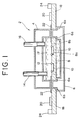
- thermal isolation means comprising a heat insulating vacuum vessel 2, which, as illustrated, has the structure of a Dewar vessel.
- the heat insulating vacuum vessel 2 is separated into an upper heat insulating vacuum portion 4 and a lower heat insulating vacuum portion 6.
- the upper and lower heat insulating vacuum portions 4 and 6 are formed, for example, of a FRP (fiber reinforced plastic) or an aluminium alloy.
- the lower heat insulating vacuum portion 6 is provided with an inner step formation 6a and an outer step formation 6b for use in supporting substrates, as will now be described.
- a multilayer ceramic substrate 8, provided with circuit patterns, is seated on the inner step formation 6a.
- the multilayer ceramic substrate 8 is provided with four recesses 8a for receiving therein first electronic devices, constituted in this example by superconducting devices 10 such as Josephson devices, and four through holes 8b to allow a cryogen to flow from an upper cavity formed above the substrate 8 to a lower cavity formed under the substrate 8, the upper and lower cavities forming a working chamber.
- the superconducting devices 10, such as Josephson devices are placed respectively in the recesses 8a and are bonded to the substrate 8 with silicone grease.
- the superconducting devices 10 are placed in the recesses 8a with the upper surfaces thereof flush with the upper surface of the multilayer ceramic substrate 8.
- the superconducting devices 10 are connected electrically to the circuit patterns of the multilayer ceramic substrate 8 by bonding wires 12 formed of an aluminum alloy. Since the upper surface of the superconducting devices 10 and the upper surface of the ceramic substrate 8 are flush with each other, the bonding wires 12 can be as short in length as 0.2mm to 0.4mm, which is advantageous for high-speed signal transmission.
- the upper heat insulating vacuum portion 4 is provided with a cryogen supply tube 14 and a cryogen discharge tube 16.
- This embodiment employs liquid helium as a cryogen. Helium gas liquefies at a temperature of about 4.2 K. Liquid helium 17 supplied through the cryogen supply tube 14 flows through the through holes 8b formed in the ceramic substrate 8 into the lower cavity under the ceramic substrate 8. Thus, the ceramic substrate 8 and the superconducting devices 10 are immersed in the liquid helium 17.
- the multilayer ceramic substrate 18 is provided with circuit patterns, and second electronic devices, in this case semiconductor devices 20 of a surface mounting type, such as flat packages and chip carriers, are mounted on the multilayer ceramic substrate 18.
- the circuit patterns of the multilayer ceramic substrate 8, and those of the multilayer ceramic substrate 18, are interconnected by film cables (connecting means) 22, as shown in Fig.5, each formed by laminating a plurality of insulating films and a plurality of conductive films.
- a plurality of coaxial connectors 24 are mounted detachably on the multilayer ceramic substrate 18.
- Figs.3 and 4 show respective sectional views of the multilayer ceramic substrates 8 and 18.
- the multilayer ceramic substrate 8 for mounting the superconducting devices is of a nine-layer structure formed by alternately laminating a plurality of signal transmitting circuit patterns 9 and a plurality of ground patterns 11, and attaching a single resistance pattern 13 for terminal matching to the bottom ground pattern 11.
- the patterns are isolated from each other by layers of ceramic.
- the respective layers of signal patterns 9, ground patterns 11 and the resistance pattern 13 are combined integrally to form the multilayer ceramic substrate 8 by burning.
- the signal patterns 9 are interconnected properly through via holes 15.
- the multilayer ceramic substrate 18 for mounting the semiconductor devices is of a five-layer structure formed by alternately laminating two signal patterns 19 and three ground patterns 21.
- the signal patterns 19 are interconnected properly through via holes 25.
- the patterns are isolated from each other by layers of ceramic.
- the respective layers of signal patterns 19 and ground patterns 21 are combined integrally to form the multilayer ceramic substrate 18 by burning.
- the characteristic impedances respectively between the signal patterns 9 and the ground patterns 11 of the multilayer ceramic substrate 8, and between the signal patterns 19 and the ground patterns 21 of the multilayer ceramic are 50 ⁇ .
- the film cable 22 is formed by alternately laminating polyimide films and conductive films formed of copper. That is, the film cable 22 is formed by laminating, from bottom to top, a polyimide film 22a, a signal pattern 22b, a polyimide film 22c, a ground pattern 22d, and a polyimide film 22e.
- the adjacent polyimide films and the conductive patterns are joined together by an adhesive, such as an epoxy resin.
- the film cable 22 consists of polyimide films and copperfoils.
- the signal pattern 22b can be formed in a structure advantageous for high-speed signal propagation, such as a strip line structure or a coplanar structure, by etching a copper foil.
- a characteristic impedance of 50 ⁇ is realized.
- the film cable 22 extends between the upper heat insulating vacuum portion 4 and the lower heat insulating portion 6 and is attached adhesively to those portions 4,6 by an adhesive 26, such as an epoxy resin.
- the signal patterns 9 and 19 of the ceramic substrates 8 and 18 are connected to the signal pattern 22b of the film cable 22 by solder portions 28.
- the ground patterns 11 and 21 of the ceramic substrates 8 and 18 are connected to the ground pattern 22d of the film cable 22 by solder at different positions.
- the copper foil forming the ground pattern 22d has the least possible thickness, for example a thickness of the order of 10 ⁇ m .
- the overall thickness of the film cable 22 is of the order of 0.1mm, so that the quantity of heat that flows from the ceramic substrate 18 through the film cable 22 to the ceramic substrate 8 can be kept to a very small value.
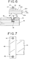
- An alternative way of connecting the signal pattern of the film cable 22 to the signal patterns of the ceramic substrate 18 will now be explained with reference to Figs. 6 and 7.
- An insulating film 30 is formed over the top ground pattern 21 to be connected to the external conductor of the coaxial connector 24 of the ceramic substrate 18, and then a plurality of contact holes for receiving contact pins 34 are formed in the ceramic substrate 18.
- caps 32 are inserted respectively in the contact holes and are soldered to the conductive film, and a contact pin 34 is put in each cap 32 with a coil spring 36 placed between the contact pin 34 and the bottom of the cap 32 so as to bias the contact pin 34 outward.
- each contact pin 34 is connected through the coil spring 36 and the cap 32 to the signal pattern 19 of the ceramic substrate 18.
- Through holes 38 are formed in the polyimide film 22a of the film cable 22 at positions respectively corresponding to the contact pins 34 to expose portions of the signal pattern 22b.
- the film cable 22 is pressed against the ceramic substrate 18 by means of a holding plate 40 employing stud bolts 42, fixed to the ceramic substrate 18, and nuts 44, so as to connect the signal pattern 22b of the film cable 22 to the signal patterns 19 of the ceramic substrate 18, through the contact pins 34, the coil springs 36 and the caps 32.
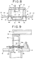
- a heat insulating vacuum vessel 2′ constituting thermal isolation means, comprises a lower heat insulating vacuum portion 50, having a depth greater than that of the lower heat insulating vacuum portion 6 of the Fig.1 apparatus, and a heat insulating vacuum lid 52 attached by adhesive 55 to the lower heat insulating portion 50, and in that the film cables 22 are inserted in the heat insulating vacuum vessel 2′ respectively through slits 50a formed respectively in the side walls of the lower heat insulating vacuum portion 50.
- the film cables 22 must be fastened firmly and closely to the lower heat insulating vacuum portion 50 in an airtight fashion by filling up gaps between the film cables 22 and the slits 50a with an adhesive 54, such as an epoxy resin, so as to maintain a vacuum within the heat insulating vacuum vessel 2′ and so to prevent a deterioration in the heat insulating function of the lower heat insulating vacuum portion 50.
- an adhesive 54 such as an epoxy resin
- heat can flow from the outside to the inside of the heat insulating vacuum vessel 2′ only thorough the film cables 22, and hence the capability of the apparatus of Figs.8 and 9 in suppressing the inflow of heat is higher than that of the apparatus of Fig.1. That is, heat flows into the heat insulating vacuum vessel 2 of Fig.1 through the walls of the upper and lower heat insulating vacuum portions 4 and 6 which adjoin the film cables 22, as well as through the film cables 22. Since the heat insulating vacuum vessel 2′ in Figs.8 and 9 has no wall corresponding to those walls, the influx of heat from outside the heat insulating vacuum vessel 2′ is very small.
- the heat insulating vacuum vessel 2 or 2′ may be evacuated by known evacuating means, and hence the description of the process of evacuating the heat insulating vacuum vessel 2, 2′ will be omitted, from this application.
- the electronic devices provided with the heat insulating vacuum vessel are connected only through the thin film cables to those disposed outside the heat insulating vacuum vessel, so that the influx into the vessel of heat generrated in the ceramic substrate having the semiconductor devices mounted thereon can be suppressed. Accordingly, the cryogen is consumed at a low rate, and hence, when the cryogen is liquid helium, even a small liquefier is sufficient for the purpose. Furthermore, since the superconducting devices and the semiconductor devices can be disposed comparatively near to each other, delay in signal propagation is negligible, so that the superconducting devices can be driven at a high speed.
- the electronic devices mounted on the ceramic substrate provided within the heat insulating vacuum vessel need not necessarily be superconducting devices, but may be HEMTs (high electron mobility transistors) or the like.
- the superconducting devices employ superconducting materials of the Y-Ba-Cu-O system which have recently been developed, liquid nitrogen may be used instead of liquid helium for cooling the superconducting devices.
Claims (5)
- Ein Gehäuse für elektronische Vorrichtungen, umfassend: wärmeisolierende Vakuumgefäßmittel (2; 2'), die das Innere davon bei einer gewünschten Temperatur halten können, die niedriger als die Umgebungstemperatur außerhalb der wärmeisolierenden Vakuumgefäßmittel (2; 2') ist; ein erstes Substrat (8), das mit einem Schaltungsmuster (9) versehen ist und darauf angebracht eine erste elektronische Vorrichtung (10) aufweist, die für einen Betrieb bei der besagten gewünschten Temperatur geeignet ist, wobei das erste Substrat (8) innerhalb der wärmeisolierenden Vakuumgefäßmittel (2; 2') angeordnet ist; ein zweites Substrat (18), das mit einem Schaltungsmuster (19) versehen ist und darauf angebracht eine zweite elektronische Vorrichtung (20) aufweist, die für einen Betrieb bei der Umgebungstemperatur geeignet ist, wobei das zweite Substrat (18) außerhalb der wärmeisolierenden Vakuumgefäßmittel (2; 2') angeordnet ist; und Verbindungsmittel (22), welche durch eine Wand der besagten wärmeisolierenden Vakuumgefäßmittel (2; 2') durchgehen und das Schaltungsmuster (9) des ersten Substrats (8) mit dem des zweiten Substrats (18) elektrisch verbinden;
dadurch gekennzeichnet, daß die ersten und zweiten Substrate (8; 18) an die wärmeisolierenden Vakuumgefäßmittel (2; 2') angebracht sind, um so jeweilige Hauptflächen aufzuweisen, welche im wesentlichen koplanar sind, so daß die Trennung zwischen gegenseitig benachbarten Rändern der besagten ersten und zweiten Substrate (8; 18) minimiert ist, und die Verbindungsmittel (22) ein Filmkabel umfassen, das auf solch eine Weise gebildet wird, um eine Wärmeübertragung daran entlang zu unterdrücken, indem eine Vielzahl elektrisch isolierender Filme (22a, 22c, 22e) und eine Vielzahl elektrisch leitender Filme (22b, 22d) abwechselnd geschichtet werden. - Ein Gehäuse nach Anspuch 1, worin die besagte erste elektronische Vorrichtung (10) eine supraleitende Vorrichtung umfaßt, wobei das Gehäuse weiter umfaßt ein kryogenes Kühlmittel, um das Innere der wärmeisolierenden Vakuumgefäßmittel (2; 2') bei einer Betriebstemperatur der supraleitenden Vorrichtung zu halten.
- Ein Gehäuse nach Anspruch 1 oder 2, worin die wärmeisolierenden Vakuumgefäßmittel (2) einen oberen wärmeisolierenden Vakuumteil (4) und einen unteren wärmeisolierenen Vakuumteil (6), getrennt von dem oberen wärmeisolierenden Vakuumteil (4), umfassen und worin das Filmkabel (22) klebend an einem unteren Bereich des oberen wärmeisolierenden Vakuumteils (4) und an einem oberen Bereich des unteren wärmeisolierenden Vakuumteils (6) angebracht ist.
- Ein Gehäuse nach Anspruch 1 oder 2, worin die wärmeisolierenden Vakuumgefäßmittel (2') ein wärmeisolierendes Vakuumgefäß (50), das mit einem Schlitz (50a) in einer Seitenwand davon versehen ist, und einen wärmeisolierenden Vakuumdeckel (52) umfassen, der klebend an dem wärmeisolierenden Vakuumgefäß (50) angebracht ist, und worin das Filmkabel (22) durch den Schlitz (50a) durchgeht und klebend an dem wärmeisolierenden Vakuumgefäß (50) befestigt ist.
- Ein Gehäuse nach irgendeinem vorhergehenden Anspruch, worin die ersten und zweiten Substrate (8, 18) Mehrschichten-Keramiksubstrate umfassen, die jeweils gebildet werden, indem signalübertragende Schaltungsmuster (9; 19) und Erdungsmuster (11; 21) abwechselnd geschichtet werden.
Applications Claiming Priority (2)
| Application Number | Priority Date | Filing Date | Title |
|---|---|---|---|
| JP63276023A JP2681288B2 (ja) | 1988-11-02 | 1988-11-02 | 超伝導素子用パッケージ |
| JP276023/88 | 1988-11-02 |
Publications (2)
| Publication Number | Publication Date |
|---|---|
| EP0367630A1 EP0367630A1 (de) | 1990-05-09 |
| EP0367630B1 true EP0367630B1 (de) | 1996-03-13 |
Family
ID=17563717
Family Applications (1)
| Application Number | Title | Priority Date | Filing Date |
|---|---|---|---|
| EP89311436A Expired - Lifetime EP0367630B1 (de) | 1988-11-02 | 1989-11-02 | Packung für elektronische Anordnungen zum Betrieb bei verschiedenen jeweiligen Temperaturen |
Country Status (4)
| Country | Link |
|---|---|
| US (1) | US4980754A (de) |
| EP (1) | EP0367630B1 (de) |
| JP (1) | JP2681288B2 (de) |
| DE (1) | DE68925939T2 (de) |
Families Citing this family (30)
| Publication number | Priority date | Publication date | Assignee | Title |
|---|---|---|---|---|
| JPH0710005B2 (ja) * | 1989-08-31 | 1995-02-01 | アメリカン テレフォン アンド テレグラフ カムパニー | 超伝導体相互接続装置 |
| US5126830A (en) * | 1989-10-31 | 1992-06-30 | General Electric Company | Cryogenic semiconductor power devices |
| US5247189A (en) * | 1989-11-15 | 1993-09-21 | Sumitomo Electric Industries, Ltd. | Superconducting device composed of oxide superconductor material |
| US5121292A (en) * | 1990-01-23 | 1992-06-09 | International Business Machines Corporation | Field replaceable cryocooled computer logic unit |
| US5212626A (en) * | 1990-11-09 | 1993-05-18 | International Business Machines Corporation | Electronic packaging and cooling system using superconductors for power distribution |
| CA2088821C (en) * | 1992-02-05 | 1999-09-07 | Hironobu Ikeda | Cooling structure for integrated circuit |
| US5474834A (en) * | 1992-03-09 | 1995-12-12 | Kyocera Corporation | Superconducting circuit sub-assembly having an oxygen shielding barrier layer |
| JPH063427A (ja) * | 1992-06-23 | 1994-01-11 | Fujitsu Ltd | 磁気検出装置 |
| US5436793A (en) * | 1993-03-31 | 1995-07-25 | Ncr Corporation | Apparatus for containing and cooling an integrated circuit device having a thermally insulative positioning member |
| US5861574A (en) * | 1993-04-14 | 1999-01-19 | Fujitsu Limited | Apparatus for mounting a superconducting element |
| JPH06350146A (ja) * | 1993-06-14 | 1994-12-22 | Sharp Corp | 超電導装置 |
| JP2953273B2 (ja) * | 1993-10-22 | 1999-09-27 | 住友電気工業株式会社 | 低温に冷却する素子の接続方法 |
| US5448108A (en) * | 1993-11-02 | 1995-09-05 | Hughes Aircraft Company | Cooling of semiconductor power modules by flushing with dielectric liquid |
| US5789704A (en) * | 1995-12-06 | 1998-08-04 | Sumitomo Wiring Systems, Ltd. | Container with heat removing features for containing an electronic contol unit |
| US6188358B1 (en) * | 1997-10-20 | 2001-02-13 | Infrared Components Corporation | Antenna signal conduit for different temperature and pressure environments |
| US6434000B1 (en) * | 1998-12-03 | 2002-08-13 | Iv Phoenix Group, Inc. | Environmental system for rugged disk drive |
| US7335965B2 (en) | 1999-08-25 | 2008-02-26 | Micron Technology, Inc. | Packaging of electronic chips with air-bridge structures |
| JP2001093821A (ja) * | 1999-09-24 | 2001-04-06 | Toshiba Corp | 製造装置組立部品、製造装置組立部品の製造方法、半導体製造装置及び電子ビーム露光装置 |
| JP4236408B2 (ja) | 2000-01-31 | 2009-03-11 | 富士通株式会社 | 熱遮断信号伝送ユニットおよび超伝導信号伝送装置 |
| CN1650467A (zh) * | 2000-09-07 | 2005-08-03 | 纳幕尔杜邦公司 | 低温装置 |
| US6744136B2 (en) * | 2001-10-29 | 2004-06-01 | International Rectifier Corporation | Sealed liquid cooled electronic device |
| US7300821B2 (en) * | 2004-08-31 | 2007-11-27 | Micron Technology, Inc. | Integrated circuit cooling and insulating device and method |
| US7202562B2 (en) * | 2004-12-02 | 2007-04-10 | Micron Technology, Inc. | Integrated circuit cooling system and method |
| US20060274502A1 (en) * | 2005-06-01 | 2006-12-07 | Rapp Robert J | Electronic package whereby an electronic assembly is packaged within an enclosure that is designed to act as a heat pipe |
| DE102014013958B4 (de) * | 2014-09-19 | 2017-06-08 | Audi Ag | Kühlanordnung für ein Kraftfahrzeugsteuergerät, Kraftfahrzeug und Kraftfahrzeugsteuergerät |
| US9524470B1 (en) * | 2015-06-12 | 2016-12-20 | International Business Machines Corporation | Modular array of vertically integrated superconducting qubit devices for scalable quantum computing |
| US9702906B2 (en) | 2015-06-26 | 2017-07-11 | International Business Machines Corporation | Non-permanent termination structure for microprobe measurements |
| US10390455B2 (en) * | 2017-03-27 | 2019-08-20 | Raytheon Company | Thermal isolation of cryo-cooled components from circuit boards or other structures |
| US11159127B2 (en) | 2019-04-30 | 2021-10-26 | Quantum Opus, LLC | Noise suppressing interface circuit for device with control circuits in different noise environments |
| US11917794B2 (en) * | 2020-10-30 | 2024-02-27 | Advanced Micro Devices, Inc. | Separating temperature domains in cooled systems |
Citations (2)
| Publication number | Priority date | Publication date | Assignee | Title |
|---|---|---|---|---|
| US4245273A (en) * | 1979-06-29 | 1981-01-13 | International Business Machines Corporation | Package for mounting and interconnecting a plurality of large scale integrated semiconductor devices |
| EP0228212A2 (de) * | 1985-12-16 | 1987-07-08 | Hitachi, Ltd. | Integriertes Halbleiterbauelement |
Family Cites Families (6)
| Publication number | Priority date | Publication date | Assignee | Title |
|---|---|---|---|---|
| JPS59144190A (ja) * | 1983-02-08 | 1984-08-18 | Agency Of Ind Science & Technol | 超伝導回路用実装基板 |
| EP0213421A3 (de) * | 1985-08-07 | 1989-02-22 | Honeywell Inc. | Infrarotdetektoranordnung mit Vakuumkammern |
| JPH0325420Y2 (de) * | 1985-10-07 | 1991-06-03 | ||
| JPH0325419Y2 (de) * | 1985-10-07 | 1991-06-03 | ||
| US4734820A (en) * | 1987-04-16 | 1988-03-29 | Ncr Corporation | Cryogenic packaging scheme |
| US4805420A (en) * | 1987-06-22 | 1989-02-21 | Ncr Corporation | Cryogenic vessel for cooling electronic components |
-
1988
- 1988-11-02 JP JP63276023A patent/JP2681288B2/ja not_active Expired - Lifetime
-
1989
- 1989-10-30 US US07/428,673 patent/US4980754A/en not_active Expired - Lifetime
- 1989-11-02 DE DE68925939T patent/DE68925939T2/de not_active Expired - Fee Related
- 1989-11-02 EP EP89311436A patent/EP0367630B1/de not_active Expired - Lifetime
Patent Citations (2)
| Publication number | Priority date | Publication date | Assignee | Title |
|---|---|---|---|---|
| US4245273A (en) * | 1979-06-29 | 1981-01-13 | International Business Machines Corporation | Package for mounting and interconnecting a plurality of large scale integrated semiconductor devices |
| EP0228212A2 (de) * | 1985-12-16 | 1987-07-08 | Hitachi, Ltd. | Integriertes Halbleiterbauelement |
Also Published As
| Publication number | Publication date |
|---|---|
| US4980754A (en) | 1990-12-25 |
| JP2681288B2 (ja) | 1997-11-26 |
| EP0367630A1 (de) | 1990-05-09 |
| DE68925939T2 (de) | 1996-08-08 |
| JPH02123774A (ja) | 1990-05-11 |
| DE68925939D1 (de) | 1996-04-18 |
Similar Documents
| Publication | Publication Date | Title |
|---|---|---|
| EP0367630B1 (de) | Packung für elektronische Anordnungen zum Betrieb bei verschiedenen jeweiligen Temperaturen | |
| EP0288022B1 (de) | Supraleitfähiges Gerät | |
| EP0340241B1 (de) | Elektronisches gehäuse zum dichten packen, bestehend aus gestapelten unterbaugruppen | |
| KR102609929B1 (ko) | 공통 기판 상에 위치된 초전도 및 비-초전도 컴포넌트를 구비한 컴퓨팅 시스템 | |
| GB2201546A (en) | Semiconductor integrated circuit device | |
| US3585455A (en) | Circuit assemblies | |
| EP0485188A1 (de) | Elektronische Packung mit einer Verbindungsplatte | |
| CN117273160A (zh) | 用于低温应用的柔性布线 | |
| EP3513631B1 (de) | Mehrschichtige leiterplatte zur reduzierung des quantensignalübersprechens | |
| US4734820A (en) | Cryogenic packaging scheme | |
| JPH07502622A (ja) | 75−80kの温度と4.5kの温度との間の電流を導くための複合リード線 | |
| EP0106936B1 (de) | Mehrdimensionale Anordnung für elektrische Packung | |
| JP2580142B2 (ja) | 多層セラミックレ−ザパッケ−ジ | |
| US4731700A (en) | Semiconductor connection and crossover apparatus | |
| EP0372108B1 (de) | Vakuumbehälter zum kryogenischen Kühlen einer Packung für eine elektronische Anordnung | |
| EP0630059B1 (de) | Supraleitende Vorrichtung mit darin integriertem Beschlag vorbeugenden Peltierelement | |
| JP2674680B2 (ja) | 超伝導超格子結晶デバイス | |
| JPH07122788A (ja) | 低温に冷却する素子の接続方法 | |
| US5747873A (en) | Technique for fabricating hybrid high-temperature superconductor-semiconductor circuits | |
| CA1269461A (en) | Low-temperature monolithic chip | |
| US11533825B2 (en) | Systems with indium application to heat transfer surfaces | |
| US20210398893A1 (en) | Quantum device | |
| JP4081834B2 (ja) | 超電導回路チップ用のチップキャリアおよびそれを用いた測定装置 | |
| JP2624673B2 (ja) | 電子機器 | |
| JPH0828533B2 (ja) | 超電導装置 |
Legal Events
| Date | Code | Title | Description |
|---|---|---|---|
| PUAI | Public reference made under article 153(3) epc to a published international application that has entered the european phase |
Free format text: ORIGINAL CODE: 0009012 |
|
| AK | Designated contracting states |
Kind code of ref document: A1 Designated state(s): DE FR GB |
|
| 17P | Request for examination filed |
Effective date: 19900515 |
|
| 17Q | First examination report despatched |
Effective date: 19920703 |
|
| GRAA | (expected) grant |
Free format text: ORIGINAL CODE: 0009210 |
|
| AK | Designated contracting states |
Kind code of ref document: B1 Designated state(s): DE FR GB |
|
| PG25 | Lapsed in a contracting state [announced via postgrant information from national office to epo] |
Ref country code: FR Effective date: 19960313 |
|
| REF | Corresponds to: |
Ref document number: 68925939 Country of ref document: DE Date of ref document: 19960418 |
|
| EN | Fr: translation not filed | ||
| PLBE | No opposition filed within time limit |
Free format text: ORIGINAL CODE: 0009261 |
|
| STAA | Information on the status of an ep patent application or granted ep patent |
Free format text: STATUS: NO OPPOSITION FILED WITHIN TIME LIMIT |
|
| 26N | No opposition filed | ||
| PGFP | Annual fee paid to national office [announced via postgrant information from national office to epo] |
Ref country code: GB Payment date: 20011031 Year of fee payment: 13 |
|
| PGFP | Annual fee paid to national office [announced via postgrant information from national office to epo] |
Ref country code: DE Payment date: 20011119 Year of fee payment: 13 |
|
| REG | Reference to a national code |
Ref country code: GB Ref legal event code: IF02 |
|
| PG25 | Lapsed in a contracting state [announced via postgrant information from national office to epo] |
Ref country code: GB Free format text: LAPSE BECAUSE OF NON-PAYMENT OF DUE FEES Effective date: 20021102 |
|
| PG25 | Lapsed in a contracting state [announced via postgrant information from national office to epo] |
Ref country code: DE Free format text: LAPSE BECAUSE OF NON-PAYMENT OF DUE FEES Effective date: 20030603 |
|
| GBPC | Gb: european patent ceased through non-payment of renewal fee |