EP0367466A2 - Abscheidungsverfahren - Google Patents
Abscheidungsverfahren Download PDFInfo
- Publication number
- EP0367466A2 EP0367466A2 EP89310869A EP89310869A EP0367466A2 EP 0367466 A2 EP0367466 A2 EP 0367466A2 EP 89310869 A EP89310869 A EP 89310869A EP 89310869 A EP89310869 A EP 89310869A EP 0367466 A2 EP0367466 A2 EP 0367466A2
- Authority
- EP
- European Patent Office
- Prior art keywords
- regions
- substrate
- layer
- spaces
- areas
- Prior art date
- Legal status (The legal status is an assumption and is not a legal conclusion. Google has not performed a legal analysis and makes no representation as to the accuracy of the status listed.)
- Withdrawn
Links
Images

Classifications
-
- G—PHYSICS
- G02—OPTICS
- G02F—OPTICAL DEVICES OR ARRANGEMENTS FOR THE CONTROL OF LIGHT BY MODIFICATION OF THE OPTICAL PROPERTIES OF THE MEDIA OF THE ELEMENTS INVOLVED THEREIN; NON-LINEAR OPTICS; FREQUENCY-CHANGING OF LIGHT; OPTICAL LOGIC ELEMENTS; OPTICAL ANALOGUE/DIGITAL CONVERTERS
- G02F1/00—Devices or arrangements for the control of the intensity, colour, phase, polarisation or direction of light arriving from an independent light source, e.g. switching, gating or modulating; Non-linear optics
- G02F1/01—Devices or arrangements for the control of the intensity, colour, phase, polarisation or direction of light arriving from an independent light source, e.g. switching, gating or modulating; Non-linear optics for the control of the intensity, phase, polarisation or colour
- G02F1/13—Devices or arrangements for the control of the intensity, colour, phase, polarisation or direction of light arriving from an independent light source, e.g. switching, gating or modulating; Non-linear optics for the control of the intensity, phase, polarisation or colour based on liquid crystals, e.g. single liquid crystal display cells
- G02F1/133—Constructional arrangements; Operation of liquid crystal cells; Circuit arrangements
- G02F1/1333—Constructional arrangements; Manufacturing methods
- G02F1/1335—Structural association of cells with optical devices, e.g. polarisers or reflectors
- G02F1/133509—Filters, e.g. light shielding masks
- G02F1/133514—Colour filters
- G02F1/133516—Methods for their manufacture, e.g. printing, electro-deposition or photolithography
-
- G—PHYSICS
- G02—OPTICS
- G02F—OPTICAL DEVICES OR ARRANGEMENTS FOR THE CONTROL OF LIGHT BY MODIFICATION OF THE OPTICAL PROPERTIES OF THE MEDIA OF THE ELEMENTS INVOLVED THEREIN; NON-LINEAR OPTICS; FREQUENCY-CHANGING OF LIGHT; OPTICAL LOGIC ELEMENTS; OPTICAL ANALOGUE/DIGITAL CONVERTERS
- G02F1/00—Devices or arrangements for the control of the intensity, colour, phase, polarisation or direction of light arriving from an independent light source, e.g. switching, gating or modulating; Non-linear optics
- G02F1/01—Devices or arrangements for the control of the intensity, colour, phase, polarisation or direction of light arriving from an independent light source, e.g. switching, gating or modulating; Non-linear optics for the control of the intensity, phase, polarisation or colour
- G02F1/13—Devices or arrangements for the control of the intensity, colour, phase, polarisation or direction of light arriving from an independent light source, e.g. switching, gating or modulating; Non-linear optics for the control of the intensity, phase, polarisation or colour based on liquid crystals, e.g. single liquid crystal display cells
- G02F1/133—Constructional arrangements; Operation of liquid crystal cells; Circuit arrangements
- G02F1/1333—Constructional arrangements; Manufacturing methods
- G02F1/1335—Structural association of cells with optical devices, e.g. polarisers or reflectors
- G02F1/133509—Filters, e.g. light shielding masks
- G02F1/133512—Light shielding layers, e.g. black matrix
Definitions
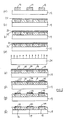
- Said first regions may be formed of dye materials and said other material may be a transparent electrically-conductive material.
- the radiation is preferably ultraviolet light.
- stripes 1, 2 and 3, or rows and columns of elemental areas, of red, green and blue dye materials are firstly deposited on a glass or other transparent substrate 4 by conventional masking and deposition techniques, leaving spaces, such as the spaces 5 and 6, therebetween.
- the substrate is to form one plate of a liquid crystal display panel.
- the dye materials may be, for example, dyed polyimide, dyed photoresist materials or gelatin-based materials. Electrodeposited materials may be used.
- the thickness of the polyimide layer is carefully controlled to give a substantially planarised layer ( Figure 1(e)) after any high temperature baking that is required.
- a further layer for example an electrically-conductive layer, may be formed on the substantially planarised layer.
- the material which is used to fill the spaces 5 and 6 of Figure 1 and 20, 21 of Figure 2 may be coloured as required, for example black, to improve the contrast of the resulting liquid crystal display.
- the material must, of course, pass the radiation wavelength which is required to activate the photosensitive material.
Landscapes
- Physics & Mathematics (AREA)
- Nonlinear Science (AREA)
- Engineering & Computer Science (AREA)
- Manufacturing & Machinery (AREA)
- Mathematical Physics (AREA)
- Chemical & Material Sciences (AREA)
- Crystallography & Structural Chemistry (AREA)
- General Physics & Mathematics (AREA)
- Optics & Photonics (AREA)
- Optical Filters (AREA)
- Liquid Crystal (AREA)
- Exposure And Positioning Against Photoresist Photosensitive Materials (AREA)
Applications Claiming Priority (2)
| Application Number | Priority Date | Filing Date | Title |
|---|---|---|---|
| GB888825826A GB8825826D0 (en) | 1988-11-04 | 1988-11-04 | Deposition processes |
| GB8825826 | 1988-11-04 |
Publications (2)
| Publication Number | Publication Date |
|---|---|
| EP0367466A2 true EP0367466A2 (de) | 1990-05-09 |
| EP0367466A3 EP0367466A3 (de) | 1991-07-24 |
Family
ID=10646303
Family Applications (1)
| Application Number | Title | Priority Date | Filing Date |
|---|---|---|---|
| EP19890310869 Withdrawn EP0367466A3 (de) | 1988-11-04 | 1989-10-23 | Abscheidungsverfahren |
Country Status (4)
| Country | Link |
|---|---|
| US (1) | US5169737A (de) |
| EP (1) | EP0367466A3 (de) |
| JP (1) | JPH02269319A (de) |
| GB (2) | GB8825826D0 (de) |
Cited By (4)
| Publication number | Priority date | Publication date | Assignee | Title |
|---|---|---|---|---|
| EP0450840A3 (en) * | 1990-04-02 | 1992-07-22 | Seiko Epson Corporation | Process for forming a colour filter |
| FR2697922A1 (fr) * | 1992-11-12 | 1994-05-13 | Gold Star Co | Procédé de fabrication d'un filtre de couleurs pour un écran à cristaux liquides. |
| EP0623944A1 (de) * | 1993-05-05 | 1994-11-09 | AT&T Corp. | Flache Bildwiedergabeanordnung und Herstellungsverfahren |
| EP1025461A4 (de) * | 1997-01-13 | 2002-04-03 | Hyundai Electronics America | Farbfilterstruktur und herstellungsverfahren |
Families Citing this family (6)
| Publication number | Priority date | Publication date | Assignee | Title |
|---|---|---|---|---|
| JP3067362B2 (ja) * | 1991-12-19 | 2000-07-17 | ソニー株式会社 | 液晶パネルの製造方法 |
| GB9203595D0 (en) * | 1992-02-20 | 1992-04-08 | Philips Electronics Uk Ltd | Methods of fabricating thin film structures and display devices produced thereby |
| KR950005442B1 (ko) * | 1992-08-24 | 1995-05-24 | 현대전자산업주식회사 | 위상반전 마스크 형성방법 |
| US5516625A (en) * | 1993-09-08 | 1996-05-14 | Harris Corporation | Fill and etchback process using dual photoresist sacrificial layer and two-step etching process for planarizing oxide-filled shallow trench structure |
| US5382317A (en) * | 1994-02-18 | 1995-01-17 | Minnesota Mining And Manufacturing Company | Method of selectively applying a coating to a bilevel substrate |
| US5529863A (en) * | 1994-08-01 | 1996-06-25 | Motorola, Inc. | Method for fabricating LCD substrates having solderable die attach pads |
Family Cites Families (8)
| Publication number | Priority date | Publication date | Assignee | Title |
|---|---|---|---|---|
| GB1377727A (en) * | 1973-06-05 | 1974-12-18 | Matsushita Electric Co Ltd | Transparent photographic film |
| NL7309451A (nl) * | 1973-07-06 | 1975-01-08 | Philips Nv | Werkwijze voor het vervaardigen van een inrichting. |
| DE2658400A1 (de) * | 1976-12-23 | 1978-06-29 | Ibm Deutschland | Verfahren zur herstellung einer negativen maske auf einem substrat |
| EP0001138A1 (de) * | 1977-08-23 | 1979-03-21 | Howard A. Fromson | Verfahren zur Herstellung von lithographischen Druckplatten |
| GB2099212B (en) * | 1981-05-19 | 1985-01-09 | Secr Defence | Manufacturing crt screens |
| JPS62160421A (ja) * | 1986-01-08 | 1987-07-16 | Shinto Paint Co Ltd | 微細な導電性回路の間に機能性塗膜を形成する方法 |
| JPH07117662B2 (ja) * | 1986-04-21 | 1995-12-18 | 神東塗料株式会社 | 微細な透明導電性回路パタ−ン上およびその間隙に機能性薄膜を形成する方法 |
| US4948706A (en) * | 1987-12-30 | 1990-08-14 | Hoya Corporation | Process for producing transparent substrate having thereon transparent conductive pattern elements separated by light-shielding insulating film, and process for producing surface-colored material |
-
1988
- 1988-11-04 GB GB888825826A patent/GB8825826D0/en active Pending
-
1989
- 1989-10-23 EP EP19890310869 patent/EP0367466A3/de not_active Withdrawn
- 1989-10-23 GB GB8923854A patent/GB2224861B/en not_active Expired - Fee Related
- 1989-10-24 US US07/426,736 patent/US5169737A/en not_active Expired - Fee Related
- 1989-11-02 JP JP1287258A patent/JPH02269319A/ja active Pending
Cited By (6)
| Publication number | Priority date | Publication date | Assignee | Title |
|---|---|---|---|---|
| EP0450840A3 (en) * | 1990-04-02 | 1992-07-22 | Seiko Epson Corporation | Process for forming a colour filter |
| FR2697922A1 (fr) * | 1992-11-12 | 1994-05-13 | Gold Star Co | Procédé de fabrication d'un filtre de couleurs pour un écran à cristaux liquides. |
| US5495354A (en) * | 1992-11-12 | 1996-02-27 | Gold Star Co., Ltd | Method of producing a color filter for a liquid crystal display by depositing metal black matrices on a transparent insulating substrate and forming color elements therebetween |
| EP0623944A1 (de) * | 1993-05-05 | 1994-11-09 | AT&T Corp. | Flache Bildwiedergabeanordnung und Herstellungsverfahren |
| US5498925A (en) * | 1993-05-05 | 1996-03-12 | At&T Corp. | Flat panel display apparatus, and method of making same |
| EP1025461A4 (de) * | 1997-01-13 | 2002-04-03 | Hyundai Electronics America | Farbfilterstruktur und herstellungsverfahren |
Also Published As
| Publication number | Publication date |
|---|---|
| GB2224861A (en) | 1990-05-16 |
| GB8923854D0 (en) | 1989-12-13 |
| EP0367466A3 (de) | 1991-07-24 |
| GB8825826D0 (en) | 1988-12-07 |
| GB2224861B (en) | 1993-03-10 |
| JPH02269319A (ja) | 1990-11-02 |
| US5169737A (en) | 1992-12-08 |
Similar Documents
| Publication | Publication Date | Title |
|---|---|---|
| EP0138459B1 (de) | Flüssigkristall-Anzeigevorrichtung mit Farbfilter | |
| US3909930A (en) | Method for fabricating a liquid crystal display device | |
| US20010007733A1 (en) | Method of manufacturing color filters and liquid crystal display device using these color filters | |
| US5169737A (en) | Deposition processes | |
| EP0523245A1 (de) | Herstellungsverfahren für vielfarbenanzeigegerät | |
| US5463484A (en) | Method for manufacturing laminated U V-sensitive color filters for liquid crystal displays | |
| CN104777665A (zh) | 黑色矩阵的制作方法 | |
| EP0471628A1 (de) | Integrierte Schaltung mit Dünnschichttransistoren und Herstellungsverfahren dafür | |
| EP0670509B1 (de) | Verfahren zur Herstellung eines Farbfilters und mehrfarbige Flüssigkristallgeräte | |
| EP0225623A2 (de) | Herstellungsverfahren eines Farbfilters | |
| KR940015536A (ko) | 액정 표시 장치의 칼라 필터 및 그 제조 방법 | |
| JPH04172304A (ja) | カラーフイルタの製造方法 | |
| US5243260A (en) | Method to produce a display screen with a matrix of transistors provided with an optical mask | |
| US5081004A (en) | Method to produce a display screen with a matrix of transistors provided with an optical mask | |
| JPH11237620A (ja) | パターン化可能な導伝性トレースを有する表示器の製造方法 | |
| EP0272194A1 (de) | Flüssigkristall-Anzeigevorrichtung mit Farbfiltern aus polychromatischem Glas | |
| RU2030775C1 (ru) | Способ изготовления многоцветного оптического фильтра для жидкокристаллического устройства | |
| KR101192752B1 (ko) | 인쇄판 및 이를 이용한 패터닝 방법 | |
| US5482590A (en) | Method for forming a display cell with counter-electrode contact pick-up | |
| KR20030057146A (ko) | 액정표시장치용 컬러필터 기판과 어레이기판 제조방법 | |
| EP0345046A2 (de) | Anzeigevorrichtung | |
| KR20010004912A (ko) | 액정 표시 장치의 컬러 필터 구조 및 그 제조방법 | |
| KR950033595A (ko) | 칼라필터 및 액정표시장치의 제조방법 | |
| JPH06331815A (ja) | カラーフィルタ | |
| JP2745544B2 (ja) | Tft型液晶表示装置の製造方法 |
Legal Events
| Date | Code | Title | Description |
|---|---|---|---|
| PUAI | Public reference made under article 153(3) epc to a published international application that has entered the european phase |
Free format text: ORIGINAL CODE: 0009012 |
|
| AK | Designated contracting states |
Kind code of ref document: A2 Designated state(s): DE FR IT NL |
|
| PUAL | Search report despatched |
Free format text: ORIGINAL CODE: 0009013 |
|
| AK | Designated contracting states |
Kind code of ref document: A3 Designated state(s): DE FR IT NL |
|
| 17P | Request for examination filed |
Effective date: 19911216 |
|
| 17Q | First examination report despatched |
Effective date: 19930922 |
|
| STAA | Information on the status of an ep patent application or granted ep patent |
Free format text: STATUS: THE APPLICATION IS DEEMED TO BE WITHDRAWN |
|
| 18D | Application deemed to be withdrawn |
Effective date: 19940203 |