US5243260A - Method to produce a display screen with a matrix of transistors provided with an optical mask - Google Patents
Method to produce a display screen with a matrix of transistors provided with an optical mask Download PDFInfo
- Publication number
- US5243260A US5243260A US07/762,594 US76259491A US5243260A US 5243260 A US5243260 A US 5243260A US 76259491 A US76259491 A US 76259491A US 5243260 A US5243260 A US 5243260A
- Authority
- US
- United States
- Prior art keywords
- layer
- resin
- transistors
- display screen
- mask
- Prior art date
- Legal status (The legal status is an assumption and is not a legal conclusion. Google has not performed a legal analysis and makes no representation as to the accuracy of the status listed.)
- Expired - Fee Related
Links
- 230000003287 optical effect Effects 0.000 title claims abstract description 20
- 239000011159 matrix material Substances 0.000 title claims abstract description 17
- 238000000034 method Methods 0.000 title abstract description 23
- 239000011347 resin Substances 0.000 claims abstract description 24
- 229920005989 resin Polymers 0.000 claims abstract description 24
- 239000004642 Polyimide Substances 0.000 claims abstract description 12
- 229910021417 amorphous silicon Inorganic materials 0.000 claims abstract description 12
- 229920001721 polyimide Polymers 0.000 claims abstract description 12
- 239000000758 substrate Substances 0.000 claims abstract description 12
- 239000003990 capacitor Substances 0.000 claims description 11
- 239000011810 insulating material Substances 0.000 claims description 10
- 238000002161 passivation Methods 0.000 claims description 3
- 239000004065 semiconductor Substances 0.000 claims 5
- 239000000975 dye Substances 0.000 claims 1
- 239000010409 thin film Substances 0.000 claims 1
- 238000000151 deposition Methods 0.000 abstract description 16
- 238000004519 manufacturing process Methods 0.000 abstract description 8
- 230000000873 masking effect Effects 0.000 abstract description 7
- HQVNEWCFYHHQES-UHFFFAOYSA-N silicon nitride Chemical compound N12[Si]34N5[Si]62N3[Si]51N64 HQVNEWCFYHHQES-UHFFFAOYSA-N 0.000 abstract description 4
- 229910052581 Si3N4 Inorganic materials 0.000 abstract description 3
- XUIMIQQOPSSXEZ-UHFFFAOYSA-N Silicon Chemical compound [Si] XUIMIQQOPSSXEZ-UHFFFAOYSA-N 0.000 abstract description 3
- 239000004411 aluminium Substances 0.000 abstract description 3
- 229910052782 aluminium Inorganic materials 0.000 abstract description 3
- XAGFODPZIPBFFR-UHFFFAOYSA-N aluminium Chemical compound [Al] XAGFODPZIPBFFR-UHFFFAOYSA-N 0.000 abstract description 3
- 229910052710 silicon Inorganic materials 0.000 abstract description 3
- 239000010703 silicon Substances 0.000 abstract description 3
- 239000004020 conductor Substances 0.000 description 7
- 239000011521 glass Substances 0.000 description 6
- 239000004973 liquid crystal related substance Substances 0.000 description 6
- 239000000463 material Substances 0.000 description 5
- 229910052751 metal Inorganic materials 0.000 description 4
- 239000002184 metal Substances 0.000 description 4
- 239000011358 absorbing material Substances 0.000 description 3
- 150000002500 ions Chemical class 0.000 description 3
- 235000008733 Citrus aurantifolia Nutrition 0.000 description 2
- DGAQECJNVWCQMB-PUAWFVPOSA-M Ilexoside XXIX Chemical compound C[C@@H]1CC[C@@]2(CC[C@@]3(C(=CC[C@H]4[C@]3(CC[C@@H]5[C@@]4(CC[C@@H](C5(C)C)OS(=O)(=O)[O-])C)C)[C@@H]2[C@]1(C)O)C)C(=O)O[C@H]6[C@@H]([C@H]([C@@H]([C@H](O6)CO)O)O)O.[Na+] DGAQECJNVWCQMB-PUAWFVPOSA-M 0.000 description 2
- 235000011941 Tilia x europaea Nutrition 0.000 description 2
- 210000004027 cell Anatomy 0.000 description 2
- 238000004040 coloring Methods 0.000 description 2
- 230000000694 effects Effects 0.000 description 2
- 238000001704 evaporation Methods 0.000 description 2
- 230000008020 evaporation Effects 0.000 description 2
- 239000004571 lime Substances 0.000 description 2
- 238000009877 rendering Methods 0.000 description 2
- 229910052708 sodium Inorganic materials 0.000 description 2
- 239000011734 sodium Substances 0.000 description 2
- VYZAMTAEIAYCRO-UHFFFAOYSA-N Chromium Chemical compound [Cr] VYZAMTAEIAYCRO-UHFFFAOYSA-N 0.000 description 1
- ATJFFYVFTNAWJD-UHFFFAOYSA-N Tin Chemical compound [Sn] ATJFFYVFTNAWJD-UHFFFAOYSA-N 0.000 description 1
- 238000002835 absorbance Methods 0.000 description 1
- 238000000137 annealing Methods 0.000 description 1
- 150000004056 anthraquinones Chemical class 0.000 description 1
- 230000002238 attenuated effect Effects 0.000 description 1
- 230000005540 biological transmission Effects 0.000 description 1
- 229910052804 chromium Inorganic materials 0.000 description 1
- 239000011651 chromium Substances 0.000 description 1
- 210000002858 crystal cell Anatomy 0.000 description 1
- 230000007547 defect Effects 0.000 description 1
- 239000012777 electrically insulating material Substances 0.000 description 1
- 229910003437 indium oxide Inorganic materials 0.000 description 1
- PJXISJQVUVHSOJ-UHFFFAOYSA-N indium(iii) oxide Chemical compound [O-2].[O-2].[O-2].[In+3].[In+3] PJXISJQVUVHSOJ-UHFFFAOYSA-N 0.000 description 1
- 150000002739 metals Chemical class 0.000 description 1
- 238000010298 pulverizing process Methods 0.000 description 1
- 239000000126 substance Substances 0.000 description 1
- 229910001887 tin oxide Inorganic materials 0.000 description 1
Images


Classifications
-
- H—ELECTRICITY
- H01—ELECTRIC ELEMENTS
- H01L—SEMICONDUCTOR DEVICES NOT COVERED BY CLASS H10
- H01L27/00—Devices consisting of a plurality of semiconductor or other solid-state components formed in or on a common substrate
- H01L27/02—Devices consisting of a plurality of semiconductor or other solid-state components formed in or on a common substrate including semiconductor components specially adapted for rectifying, oscillating, amplifying or switching and having at least one potential-jump barrier or surface barrier; including integrated passive circuit elements with at least one potential-jump barrier or surface barrier
- H01L27/12—Devices consisting of a plurality of semiconductor or other solid-state components formed in or on a common substrate including semiconductor components specially adapted for rectifying, oscillating, amplifying or switching and having at least one potential-jump barrier or surface barrier; including integrated passive circuit elements with at least one potential-jump barrier or surface barrier the substrate being other than a semiconductor body, e.g. an insulating body
- H01L27/1214—Devices consisting of a plurality of semiconductor or other solid-state components formed in or on a common substrate including semiconductor components specially adapted for rectifying, oscillating, amplifying or switching and having at least one potential-jump barrier or surface barrier; including integrated passive circuit elements with at least one potential-jump barrier or surface barrier the substrate being other than a semiconductor body, e.g. an insulating body comprising a plurality of TFTs formed on a non-semiconducting substrate, e.g. driving circuits for AMLCDs
- H01L27/1259—Multistep manufacturing methods
- H01L27/1288—Multistep manufacturing methods employing particular masking sequences or specially adapted masks, e.g. half-tone mask
-
- G—PHYSICS
- G02—OPTICS
- G02F—OPTICAL DEVICES OR ARRANGEMENTS FOR THE CONTROL OF LIGHT BY MODIFICATION OF THE OPTICAL PROPERTIES OF THE MEDIA OF THE ELEMENTS INVOLVED THEREIN; NON-LINEAR OPTICS; FREQUENCY-CHANGING OF LIGHT; OPTICAL LOGIC ELEMENTS; OPTICAL ANALOGUE/DIGITAL CONVERTERS
- G02F1/00—Devices or arrangements for the control of the intensity, colour, phase, polarisation or direction of light arriving from an independent light source, e.g. switching, gating or modulating; Non-linear optics
- G02F1/01—Devices or arrangements for the control of the intensity, colour, phase, polarisation or direction of light arriving from an independent light source, e.g. switching, gating or modulating; Non-linear optics for the control of the intensity, phase, polarisation or colour
- G02F1/13—Devices or arrangements for the control of the intensity, colour, phase, polarisation or direction of light arriving from an independent light source, e.g. switching, gating or modulating; Non-linear optics for the control of the intensity, phase, polarisation or colour based on liquid crystals, e.g. single liquid crystal display cells
- G02F1/133—Constructional arrangements; Operation of liquid crystal cells; Circuit arrangements
- G02F1/136—Liquid crystal cells structurally associated with a semi-conducting layer or substrate, e.g. cells forming part of an integrated circuit
- G02F1/1362—Active matrix addressed cells
- G02F1/136209—Light shielding layers, e.g. black matrix, incorporated in the active matrix substrate, e.g. structurally associated with the switching element
-
- H—ELECTRICITY
- H01—ELECTRIC ELEMENTS
- H01L—SEMICONDUCTOR DEVICES NOT COVERED BY CLASS H10
- H01L27/00—Devices consisting of a plurality of semiconductor or other solid-state components formed in or on a common substrate
- H01L27/02—Devices consisting of a plurality of semiconductor or other solid-state components formed in or on a common substrate including semiconductor components specially adapted for rectifying, oscillating, amplifying or switching and having at least one potential-jump barrier or surface barrier; including integrated passive circuit elements with at least one potential-jump barrier or surface barrier
- H01L27/12—Devices consisting of a plurality of semiconductor or other solid-state components formed in or on a common substrate including semiconductor components specially adapted for rectifying, oscillating, amplifying or switching and having at least one potential-jump barrier or surface barrier; including integrated passive circuit elements with at least one potential-jump barrier or surface barrier the substrate being other than a semiconductor body, e.g. an insulating body
- H01L27/1214—Devices consisting of a plurality of semiconductor or other solid-state components formed in or on a common substrate including semiconductor components specially adapted for rectifying, oscillating, amplifying or switching and having at least one potential-jump barrier or surface barrier; including integrated passive circuit elements with at least one potential-jump barrier or surface barrier the substrate being other than a semiconductor body, e.g. an insulating body comprising a plurality of TFTs formed on a non-semiconducting substrate, e.g. driving circuits for AMLCDs
-
- H—ELECTRICITY
- H01—ELECTRIC ELEMENTS
- H01L—SEMICONDUCTOR DEVICES NOT COVERED BY CLASS H10
- H01L29/00—Semiconductor devices adapted for rectifying, amplifying, oscillating or switching, or capacitors or resistors with at least one potential-jump barrier or surface barrier, e.g. PN junction depletion layer or carrier concentration layer; Details of semiconductor bodies or of electrodes thereof ; Multistep manufacturing processes therefor
- H01L29/66—Types of semiconductor device ; Multistep manufacturing processes therefor
- H01L29/68—Types of semiconductor device ; Multistep manufacturing processes therefor controllable by only the electric current supplied, or only the electric potential applied, to an electrode which does not carry the current to be rectified, amplified or switched
- H01L29/76—Unipolar devices, e.g. field effect transistors
- H01L29/772—Field effect transistors
- H01L29/78—Field effect transistors with field effect produced by an insulated gate
- H01L29/786—Thin film transistors, i.e. transistors with a channel being at least partly a thin film
- H01L29/78651—Silicon transistors
- H01L29/7866—Non-monocrystalline silicon transistors
- H01L29/78663—Amorphous silicon transistors
- H01L29/78666—Amorphous silicon transistors with normal-type structure, e.g. with top gate
-
- G—PHYSICS
- G02—OPTICS
- G02F—OPTICAL DEVICES OR ARRANGEMENTS FOR THE CONTROL OF LIGHT BY MODIFICATION OF THE OPTICAL PROPERTIES OF THE MEDIA OF THE ELEMENTS INVOLVED THEREIN; NON-LINEAR OPTICS; FREQUENCY-CHANGING OF LIGHT; OPTICAL LOGIC ELEMENTS; OPTICAL ANALOGUE/DIGITAL CONVERTERS
- G02F1/00—Devices or arrangements for the control of the intensity, colour, phase, polarisation or direction of light arriving from an independent light source, e.g. switching, gating or modulating; Non-linear optics
- G02F1/01—Devices or arrangements for the control of the intensity, colour, phase, polarisation or direction of light arriving from an independent light source, e.g. switching, gating or modulating; Non-linear optics for the control of the intensity, phase, polarisation or colour
- G02F1/13—Devices or arrangements for the control of the intensity, colour, phase, polarisation or direction of light arriving from an independent light source, e.g. switching, gating or modulating; Non-linear optics for the control of the intensity, phase, polarisation or colour based on liquid crystals, e.g. single liquid crystal display cells
- G02F1/133—Constructional arrangements; Operation of liquid crystal cells; Circuit arrangements
- G02F1/1333—Constructional arrangements; Manufacturing methods
- G02F1/1335—Structural association of cells with optical devices, e.g. polarisers or reflectors
- G02F1/133509—Filters, e.g. light shielding masks
- G02F1/133512—Light shielding layers, e.g. black matrix
-
- G—PHYSICS
- G02—OPTICS
- G02F—OPTICAL DEVICES OR ARRANGEMENTS FOR THE CONTROL OF LIGHT BY MODIFICATION OF THE OPTICAL PROPERTIES OF THE MEDIA OF THE ELEMENTS INVOLVED THEREIN; NON-LINEAR OPTICS; FREQUENCY-CHANGING OF LIGHT; OPTICAL LOGIC ELEMENTS; OPTICAL ANALOGUE/DIGITAL CONVERTERS
- G02F2202/00—Materials and properties
- G02F2202/02—Materials and properties organic material
- G02F2202/022—Materials and properties organic material polymeric
-
- G—PHYSICS
- G02—OPTICS
- G02F—OPTICAL DEVICES OR ARRANGEMENTS FOR THE CONTROL OF LIGHT BY MODIFICATION OF THE OPTICAL PROPERTIES OF THE MEDIA OF THE ELEMENTS INVOLVED THEREIN; NON-LINEAR OPTICS; FREQUENCY-CHANGING OF LIGHT; OPTICAL LOGIC ELEMENTS; OPTICAL ANALOGUE/DIGITAL CONVERTERS
- G02F2202/00—Materials and properties
- G02F2202/10—Materials and properties semiconductor
- G02F2202/103—Materials and properties semiconductor a-Si
Definitions
- the object of the present invention is to provide a method to produce an active matrix display screen based on capacitors and thin layers of transistors, said transistors being provided with an optical mask.
- the present invention is applicable in particular to the embodiment of liquid crystal display circuits.
- Circuits with thin layers of transistors are mainly used in the production of active matrix display screens.
- an electronic memory formed of memory points distributed over the entire surface of the screen stores the video signal throughout the duration of the image.
- the electrooptical transducer (for example, a liquid crystal) is in contact with each memory point and is excited throughout the duration of an image, whereas, in systems without any electronic memory, the transducer is only excited during the duration of a line.
- the optical effect and the authorized multiplexing rate are accordingly much more significant.
- the TLTs make it possible to embody such an electronic memory on a glass substrate.
- Each memory point is situated at the crossing of one line and one connection column and is constituted of two parallel transistors and a capacitor.
- the armatures of the capacitor may be constituted by the electrodes of the liquid crystal cell itself. The memory point is thus brought back to two TLTs and one capacitor, one of the armatures of said capacitor being constituted by an electrode disposed on the wall of the cell which contains the TLTs, the other armature being constituted by the counter-electrode disposed on the other wall of the cell.
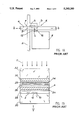
- FIG. 1 Such a structure is represented on FIG. 1 wherein FIG. 1A is a top view of one point of the active matrix and FIG. 1B is a sectional view along the line b--b of FIG. 1A.
- FIG. 1A shows a conductive column 2 and a conductive line 4 constituting the addressing columns and lines of the points of the active matrix, two TLTs 6 and 7 in parallel, and one transparent electrode 8 constituting one of the armatures of the capacitors or elementary display points of the active matrix.
- Each column 2 is provided with a cross 10 and each electrode 8 with a finger 12.
- the crossings of the line 4 with the column 2 and the cross 10 defining the drains D of the TLTs and the crossing of the line 4 with the finger 12 define the source S of the TLTs.
- the part of the line 4 situated between the column 2 and the cross 10 constitute the gate G of the TLTs.
- FIG. 1B shows firstly a lower insulating and transparent wall 20 bearing the column 2, the finger 12 of the elementary display point and the cross 10; these conductive elements 2, 10 and 12 are covered by a layer of hydrogenated amorphous silicon 22 and then an insulating gate layer 24 supporting the conductive lines 4. This unit is covered with a self-aligning layer 26 intended to be in contact with the electro-optical material 28 (liquid crystal).
- the display screen includes a transparent counter-electrode 30 supported by an upper insulating transparent wall 32.
- colored filters 34 usually about three (red, blue and green), need to be provided on the counter-electrode 30 and be in contact with the material 28.
- TLTs may be embodied with TLTs and, for example, all or part of the registers to be offset.
- This screen is intended to be lit up via the rear with fluorescent tubes and display is designed to be observed via the lower face, as shown on part B of FIG. 1.
- the gate metal namely the one constituting the lines 4, ensures protection of the TLTs 6 against the rear light of the display screen.
- the "underside" of the TLTs is exposed to the ambient observation light. If this light is intense, a photo-current is generated in the amorphous silicon layer 22 reducing the contrast of the screen as the Ion/Ioff ratio diminishes; Ion and Ioff respectively represent the currents delivered by the transistors of one displayed point and one non-displayed point.
- amorphous silicon of low thickness ⁇ 50 nm
- this photo-current is attenuated but is nevertheless adequate so as to reduce the contrast.
- an optical mask needs to be provided under the transistors so as to use the screen with the ambient light and thus ensuring a constant image.
- a metal is generally used which is engraved.
- a passivation layer is required. Such a structure is described in the article in Japan Display 1983, p. 211 by Canon.
- This technique requires the use of two depositings under vacuum, which is relatively constricting, as well as a specific masking level so as to define the form and location of the optical mask under the transistors.
- This additional masking level strictly requires self-aligning accuracy of this mask with respect to the source and drain contact of the transistors. Accordingly, this technique is complex and delicate.
- the object therefore of the invention is to overcome these drawbacks by providing an optical mask of the "underside" of the transistors with an active matrix, while reducing the number of masking levels and by ensuring a self-positioning of these optical masks with respect to the sources and drains of the transistors.
- the object of the invention is to provide a method to produce an active matrix display screen formed of points each constituted by a transistor consisting of thin layers and a capacitor and comprising conductive lines and columns for the addressing of the points, said method consisting of:
- the method of the invention does not comprise any critical stage and solely comprises two masking levels. It makes it possible to suppress the photo-current of the thin-layered transistors due to the ambient lighting of the display screen.
- the method of the invention also makes it possible to use a relatively thick (>200 nm) amorphous silicon layer, which provides a more improved material and in particular control of its less critical thickness.
- the channel of the transistors is laid on an absorbing and electrically insulating material block which also serves as a passivation material.
- the insulating substrate is made of glass.
- a low-priced glass can be used, such as lime/sodium glass, thus reducing the cost of the display screen.
- the absorbing material is a polymerizable resin containing opaque colorings, the polylmerization of this resin in particular being effected immediately before depositing the hydrogenated amorphous silicon layer.
- the object of the invention is also to provide an active matrix display screen obtained by the previously described method.
- this matrix is formed on an electric insulating substrate and comprises points, conductive lines and columns for addressing of the points, each point being constituted by a capacitor and a thin-layered transistor mainly including an optical mask made of an electric insulating material situated under the channel of the transistor and directly on the substrate, one source and one drain both self-positioned with respect to the optical mask and in direct contact with the substrate, as well as a gate surmounting the optical mask and separated from the latter by the stacked hydrogenated amorphous silicon and an electric insulating material, the amorphous silicon being in contact with the source and the drain.
- the technique for producing the sources and drains in the method of the invention ensures a self-positioning of the sources and drains of the transistors with respect to the optical mask of the latter. Furthermore, if the thickness of the absorbing material and the first conductive material, in which the sources and drains of the transistors are defined, is selected carefully and correctly, a plane structure is obtained under the hydrogenated amorphous silicon, that is a step-free structure, it being a known fact that the passages of steps can be sources of defects in the transistors and with the environments of addressing lines and columns.
- FIGS. 1A and 1B show a top plan view of one point of the active matrix and a sectional view of the various stages of the prior art method, respectively,
- FIGS. 2A-1E show a sectional view of the various stages of the method of the invention applied to the production of a liquid crystal display screen
- FIG. 3 shows a top view of the front face of a display screen obtained by the method of the invention
- FIG. 4 shows a top view of the front face of a display screen obtained by the methods according to the prior Art.
- the first stage for producing an optically masked thin-layered transistor consists, as shown on part A of FIG. 2, of depositing with a plate whirler on a lime/sodium type glass substrate 100 a layer of polyimide 102 containing colorings from the family of anthraquinones, azo compounds and phthalocyanines so as to render this polyimide layer opaque and then of prepolymerizing the latter at 150° C. for 30 minutes.
- the polyimide is preferably the one commercialized by BREWER SCIENCE, P.O. Box GG ROLLA, Mo. 65401, USA.
- a layer of positive photosensitive resin is deposited (for example, the SHIPLEY 1350H type) which is dried at 100° C. for 30 minutes.
- This resin is then insolated through a negative mask 105 ensuring masking of the channel of the transistor to be embodied, this insolation being effected with ultraviolets rays.
- the exposed resin is developed, the aim of this being to eliminate the exposed resin and to solubilize the polyimide not protected by the exposed resin.
- the structure obtained is the one represented on part B.
- the developer used is, for example, the SHIPLEY MF 312 developer.
- a transparent conductive layer 106 is deposited by evaporation, such layer being, for example, a layer of tin and indium oxide, and possibly a layer of metal 108, such as chromium, so as to subsequently obtain the level 1 of the plane structure (FIG. D).
- the overall thickness of the layers 106 and 108 needs to be equal to the thickness of the polyimide layer 102.
- the layer 102 may have a thickness of 1000 nm, the layer 106 a thickness of 700 nm and the layer 108 a thickness of 300 nm.
- the layers 106 and 108 are deposited on the unit of the structure, that is on the exposed parts of the structure 100 and on the remaining resin 104.
- the resin 104 is dissolved in the BREWER SCIENCE stripper, thus eliminating the metals 106 and 108 deposited on the resin.
- the respective source and drain contacts S and D of the thin-layered transistor are obtained and the channel of the transistor is laid bare, as shown on part D of FIG. 2.
- an annealing under vacuum is subsequently carried out up to a temperature of about 400° C. so as to polymerize all the remaining black polyimide 102 without resulting in any significant loss of the absorbance of this material.
- Production of the transistor is continued, as shown on part E of FIG. 2, by depositing a layer of hydrogenated amorphous silicon 110, a layer of silicon nitride 112 and finally a layer of aluminium 114 on the unit of the structure.
- the layers 110 and 112 are obtained by means of plasma enhanced chemical vapor depositing (PECVD), the aluminium 114 being deposited by evaporation or pulverization. Then an engraving is carried out of the stack of the layers 114, 112, 110 and 108 by conventional means so as to define the gate of the transistor.
- PECVD plasma enhanced chemical vapor depositing
- the final stage of the method consists of rendering passive the unit of the structure by depositing a layer of silicon nitride 116.
- the method described with reference to FIG. 2 is compatible with the method for producing an active matrix display screen described in the document EP-A-O-103-523 and in the document FR-A-2 571 893.
- the negative mask 105 used to mask the channel of the transistors is also used to mask one of the armatures of the capacitors, as well as the conductive columns of the display screen to be embodied.
- These armatures 8 and columns 2 are then formed at the same time as the source and drain contacts of the transistors by means of the "lift-off" technique.
- the addressing lines 4 of the display screen are simultaneously formed at the gate of the transistor in the conductive layer 114.
- FIG. 3 shows a top view of the front face of one part of a display screen obtained by the method of the invention. This figure also shows the addressing columns 2, the ITO transparent electrodes 8, the crosses 10 integral with the columns 2, and the fingers 12 of the display points integral with the electrodes 8.
- the method of the invention makes it possible to cover all the zones around the electrodes 8 and the columns 2, respectively equipped with their fingers 12 and crosses 10 the columns 2, respectively equipped with their fingers 12 and crosses 10, with black polyimide 102. It is then possible to deposit an optical mask, symbolized by the dot-and-dash lines shown on FIG. 3 and bearing the reference 120, on the counter-electrode 30 (FIG. 1) slightly wider than the columns 2 without resulting in any critical alignment of the counter-electrode 30 with respect to the active matrix, so that the elementary display points 8 transmit the light.
- the opening percentage of the display screen corresponding to the light transmission percentage is the ratio of the actual effective surface area to display on the total screen surface.
- the effective surface area 121 is equal to the surface of the electrodes 8. In this case, the opening percentage is 71%.
Abstract
Description
Claims (5)
Priority Applications (1)
| Application Number | Priority Date | Filing Date | Title |
|---|---|---|---|
| US07/762,594 US5243260A (en) | 1988-11-08 | 1991-09-19 | Method to produce a display screen with a matrix of transistors provided with an optical mask |
Applications Claiming Priority (4)
| Application Number | Priority Date | Filing Date | Title |
|---|---|---|---|
| FR8814562A FR2638880B1 (en) | 1988-11-08 | 1988-11-08 | METHOD FOR MANUFACTURING A MATRIX DISPLAY SCREEN WITH TRANSISTORS PROVIDED WITH AN OPTICAL MASK |
| FR8814562 | 1988-11-08 | ||
| US07/430,890 US5081004A (en) | 1988-11-08 | 1989-11-02 | Method to produce a display screen with a matrix of transistors provided with an optical mask |
| US07/762,594 US5243260A (en) | 1988-11-08 | 1991-09-19 | Method to produce a display screen with a matrix of transistors provided with an optical mask |
Related Parent Applications (1)
| Application Number | Title | Priority Date | Filing Date |
|---|---|---|---|
| US07/430,890 Division US5081004A (en) | 1988-11-08 | 1989-11-02 | Method to produce a display screen with a matrix of transistors provided with an optical mask |
Publications (1)
| Publication Number | Publication Date |
|---|---|
| US5243260A true US5243260A (en) | 1993-09-07 |
Family
ID=27251724
Family Applications (1)
| Application Number | Title | Priority Date | Filing Date |
|---|---|---|---|
| US07/762,594 Expired - Fee Related US5243260A (en) | 1988-11-08 | 1991-09-19 | Method to produce a display screen with a matrix of transistors provided with an optical mask |
Country Status (1)
| Country | Link |
|---|---|
| US (1) | US5243260A (en) |
Cited By (8)
| Publication number | Priority date | Publication date | Assignee | Title |
|---|---|---|---|---|
| WO1995023397A2 (en) * | 1994-02-18 | 1995-08-31 | Philips Electronics N.V. | Method of manufacturing a reflective display |
| US5652667A (en) * | 1995-02-03 | 1997-07-29 | Victor Company Of Japan, Ltd. | Liquid crystal display apparatus |
| US5691782A (en) * | 1994-07-08 | 1997-11-25 | Sanyo Electric Co., Ltd. | Liquid-crystal display with inter-line short-circuit preventive function and process for producing same |
| US6052165A (en) * | 1997-12-22 | 2000-04-18 | Philips Electronics North America Corporation | Reflective liquid crystal display (LCD) device having an internal reflection reducer |
| US20030102478A1 (en) * | 2001-11-02 | 2003-06-05 | Seung Ki Joo | Storage capacitor structure for LCD and OELD panels |
| US6618409B1 (en) * | 2000-05-03 | 2003-09-09 | Corning Incorporated | Passivation of semiconductor laser facets |
| US20040200976A1 (en) * | 2003-04-08 | 2004-10-14 | Fuji Xerox Co., Ltd. | Light detecting device and method for mounting the same |
| US20040200951A1 (en) * | 2003-04-08 | 2004-10-14 | Fuji Xerox Co., Ltd. | Light detection device and mounting method thereof |
Citations (6)
| Publication number | Priority date | Publication date | Assignee | Title |
|---|---|---|---|---|
| US4704559A (en) * | 1986-02-25 | 1987-11-03 | Seiko Instruments & Electronics Ltd. | Matrix type multi-color display device |
| US4902638A (en) * | 1985-04-23 | 1990-02-20 | Asahi Glass Company, Ltd. | Thin film transistor, method of repairing the thin film transistor and display apparatus having the thin film transistor |
| US5028122A (en) * | 1988-04-20 | 1991-07-02 | Sharp Kabushiki Kaisha | Liquid crystal active-matrix display device |
| US5040875A (en) * | 1987-07-22 | 1991-08-20 | Nec Corporation | Active matrix liquid crystal display having a high contrast ratio |
| US5066106A (en) * | 1988-01-27 | 1991-11-19 | Mitsubishi Denki Kabushiki Kaisha | Liquid crystal display device having redundant buses |
| US5087113A (en) * | 1988-02-25 | 1992-02-11 | Sharp Kabushiki Kaisha | Liquid crystal display device |
-
1991
- 1991-09-19 US US07/762,594 patent/US5243260A/en not_active Expired - Fee Related
Patent Citations (7)
| Publication number | Priority date | Publication date | Assignee | Title |
|---|---|---|---|---|
| US4902638A (en) * | 1985-04-23 | 1990-02-20 | Asahi Glass Company, Ltd. | Thin film transistor, method of repairing the thin film transistor and display apparatus having the thin film transistor |
| US4907861A (en) * | 1985-04-23 | 1990-03-13 | Asahi Glass Company Ltd. | Thin film transistor, method of repairing the film transistor and display apparatus having the thin film transistor |
| US4704559A (en) * | 1986-02-25 | 1987-11-03 | Seiko Instruments & Electronics Ltd. | Matrix type multi-color display device |
| US5040875A (en) * | 1987-07-22 | 1991-08-20 | Nec Corporation | Active matrix liquid crystal display having a high contrast ratio |
| US5066106A (en) * | 1988-01-27 | 1991-11-19 | Mitsubishi Denki Kabushiki Kaisha | Liquid crystal display device having redundant buses |
| US5087113A (en) * | 1988-02-25 | 1992-02-11 | Sharp Kabushiki Kaisha | Liquid crystal display device |
| US5028122A (en) * | 1988-04-20 | 1991-07-02 | Sharp Kabushiki Kaisha | Liquid crystal active-matrix display device |
Cited By (12)
| Publication number | Priority date | Publication date | Assignee | Title |
|---|---|---|---|---|
| WO1995023397A2 (en) * | 1994-02-18 | 1995-08-31 | Philips Electronics N.V. | Method of manufacturing a reflective display |
| WO1995023397A3 (en) * | 1994-02-18 | 1995-10-26 | Philips Electronics Nv | Method of manufacturing a reflective display |
| US5691782A (en) * | 1994-07-08 | 1997-11-25 | Sanyo Electric Co., Ltd. | Liquid-crystal display with inter-line short-circuit preventive function and process for producing same |
| US5652667A (en) * | 1995-02-03 | 1997-07-29 | Victor Company Of Japan, Ltd. | Liquid crystal display apparatus |
| US6052165A (en) * | 1997-12-22 | 2000-04-18 | Philips Electronics North America Corporation | Reflective liquid crystal display (LCD) device having an internal reflection reducer |
| US6618409B1 (en) * | 2000-05-03 | 2003-09-09 | Corning Incorporated | Passivation of semiconductor laser facets |
| US20030102478A1 (en) * | 2001-11-02 | 2003-06-05 | Seung Ki Joo | Storage capacitor structure for LCD and OELD panels |
| US6833561B2 (en) * | 2001-11-02 | 2004-12-21 | Seung Ki Joo | Storage capacitor structure for LCD and OELD panels |
| US20040200976A1 (en) * | 2003-04-08 | 2004-10-14 | Fuji Xerox Co., Ltd. | Light detecting device and method for mounting the same |
| US20040200951A1 (en) * | 2003-04-08 | 2004-10-14 | Fuji Xerox Co., Ltd. | Light detection device and mounting method thereof |
| US7095089B2 (en) * | 2003-04-08 | 2006-08-22 | Fuji Xerox Co., Ltd. | Light detecting device and method for mounting the same |
| US7173232B2 (en) * | 2003-04-08 | 2007-02-06 | Fuji Xerox Co., Ltd. | Light detection device and mounting method thereof |
Similar Documents
| Publication | Publication Date | Title |
|---|---|---|
| US5917571A (en) | Active matrix substrate having benzocyclobutene-containing interlayer insulating film and method for fabricating same | |
| KR100270127B1 (en) | Lcd apparatus | |
| CN100507695C (en) | Method for fabricating liquid crystal display device | |
| KR100868771B1 (en) | Liquid crystal display device | |
| TWI423444B (en) | Thin film transistor array panel and manufacturing method thereof | |
| JP2001142061A (en) | Active matrix type liquid crystal display device | |
| JPH11133450A (en) | Liquid crystal display device and its production | |
| GB2212661A (en) | Method of manufacturing an amorphous-silicon thin-film transistor | |
| KR19980077392A (en) | Thin film transistor liquid crystal display and manufacturing method thereof | |
| JP2001296557A (en) | Thin film transistor substrate for liquid crystal display device, and manufacturing method therefor | |
| US20060290830A1 (en) | Semi-transmissive liquid crystal display device and method of manufacture thereof | |
| US20010026342A1 (en) | Method of manufacturing an electrode substrate resistant to wire breakage for an active matrix display device | |
| US6037084A (en) | Method of making a color filter plate with multi-gap for LCD | |
| US5243260A (en) | Method to produce a display screen with a matrix of transistors provided with an optical mask | |
| US5081004A (en) | Method to produce a display screen with a matrix of transistors provided with an optical mask | |
| GB2213974A (en) | Liquid crystal display devices | |
| EP1576415B1 (en) | Liquid crystal displays | |
| KR100237673B1 (en) | Liquid crystal display device and manufacturing method | |
| JP2001264798A (en) | Active matrix substrate and optical modulation device using the same | |
| JPH1031230A (en) | Manufacture of array substrate for display device | |
| KR100569715B1 (en) | Method of manufacturing flat drive liquid crystal display | |
| KR100603852B1 (en) | Method for manufacturing liquid crystal display device using diffraction exposure technique | |
| KR100951731B1 (en) | TFT-LCD and method for manufacturing the same | |
| JPH08152612A (en) | Liquid crystal display device | |
| KR100309213B1 (en) | A method for manufacturing an lcd using a diffarctive expos ure |
Legal Events
| Date | Code | Title | Description |
|---|---|---|---|
| FEPP | Fee payment procedure |
Free format text: PAYOR NUMBER ASSIGNED (ORIGINAL EVENT CODE: ASPN); ENTITY STATUS OF PATENT OWNER: LARGE ENTITY |
|
| AS | Assignment |
Owner name: FRANCE TELECOM, ETABLISSEMENT AUTONOME DE DROIT PU Free format text: ASSIGNMENT OF ASSIGNORS INTEREST;ASSIGNOR:CENTRE NATIONAL D'ETUDES DES TELECOMMUNICATIONS;REEL/FRAME:006993/0798 Effective date: 19940407 |
|
| FPAY | Fee payment |
Year of fee payment: 4 |
|
| FEPP | Fee payment procedure |
Free format text: PAYER NUMBER DE-ASSIGNED (ORIGINAL EVENT CODE: RMPN); ENTITY STATUS OF PATENT OWNER: LARGE ENTITY |
|
| FPAY | Fee payment |
Year of fee payment: 8 |
|
| REMI | Maintenance fee reminder mailed | ||
| LAPS | Lapse for failure to pay maintenance fees | ||
| STCH | Information on status: patent discontinuation |
Free format text: PATENT EXPIRED DUE TO NONPAYMENT OF MAINTENANCE FEES UNDER 37 CFR 1.362 |
|
| FP | Lapsed due to failure to pay maintenance fee |
Effective date: 20050907 |