EP0366359A2 - Leistungsverbrauchsverringerung in On-Chip-Speicheranordnungen - Google Patents
Leistungsverbrauchsverringerung in On-Chip-Speicheranordnungen Download PDFInfo
- Publication number
- EP0366359A2 EP0366359A2 EP89310758A EP89310758A EP0366359A2 EP 0366359 A2 EP0366359 A2 EP 0366359A2 EP 89310758 A EP89310758 A EP 89310758A EP 89310758 A EP89310758 A EP 89310758A EP 0366359 A2 EP0366359 A2 EP 0366359A2
- Authority
- EP
- European Patent Office
- Prior art keywords
- word line
- line address
- word
- bit
- clock
- Prior art date
- Legal status (The legal status is an assumption and is not a legal conclusion. Google has not performed a legal analysis and makes no representation as to the accuracy of the status listed.)
- Granted
Links
- 230000008859 change Effects 0.000 claims abstract description 28
- 239000004065 semiconductor Substances 0.000 claims abstract description 23
- 230000015654 memory Effects 0.000 claims description 96
- 238000011156 evaluation Methods 0.000 claims description 17
- 238000001514 detection method Methods 0.000 claims description 9
- 230000004913 activation Effects 0.000 claims description 3
- 230000003247 decreasing effect Effects 0.000 abstract 1
- 230000009467 reduction Effects 0.000 description 13
- 238000010586 diagram Methods 0.000 description 11
- 230000004048 modification Effects 0.000 description 5
- 238000012986 modification Methods 0.000 description 5
- 230000001360 synchronised effect Effects 0.000 description 5
- 230000000694 effects Effects 0.000 description 2
- 238000005516 engineering process Methods 0.000 description 2
- 238000012544 monitoring process Methods 0.000 description 2
- 230000002411 adverse Effects 0.000 description 1
- 230000003750 conditioning effect Effects 0.000 description 1
- 239000000470 constituent Substances 0.000 description 1
- 230000009849 deactivation Effects 0.000 description 1
- 230000001419 dependent effect Effects 0.000 description 1
- 238000013461 design Methods 0.000 description 1
- 238000007599 discharging Methods 0.000 description 1
- 238000010304 firing Methods 0.000 description 1
- 230000006870 function Effects 0.000 description 1
- 238000004519 manufacturing process Methods 0.000 description 1
- 239000011159 matrix material Substances 0.000 description 1
- 230000003071 parasitic effect Effects 0.000 description 1
- 238000012545 processing Methods 0.000 description 1
Images

Classifications
-
- G—PHYSICS
- G11—INFORMATION STORAGE
- G11C—STATIC STORES
- G11C8/00—Arrangements for selecting an address in a digital store
- G11C8/18—Address timing or clocking circuits; Address control signal generation or management, e.g. for row address strobe [RAS] or column address strobe [CAS] signals
-
- G—PHYSICS
- G11—INFORMATION STORAGE
- G11C—STATIC STORES
- G11C7/00—Arrangements for writing information into, or reading information out from, a digital store
- G11C7/12—Bit line control circuits, e.g. drivers, boosters, pull-up circuits, pull-down circuits, precharging circuits, equalising circuits, for bit lines
Definitions
- the present invention relates to semiconductor memories, and more particularly to improvements in semiconductor memories of the type integrated on-chip in large scale and very large scale semiconductor monolithic integrated circuits, such improvements being directed to, and affording, reduced power consumption.
- a semiconductor memory of the "on-chip” type is a memory disposed and arranged within the chip (i.e., the semiconductor body) of a monolithic integrated circuit in integral association with other portions of the body constituting, for example, the master clock, logic, control, and other functional portions of the total circuit.
- Such an on-chip memory is to be distinguished from a semiconductor memory of the stand-alone type, where in effect the semiconductor body containing the memory constitutes only the memory, and does not include other significant portions not directly associated and involved with the functioning of the memory.
- on-chip semiconductor memories and those of the stand-alone type derive from the fact that a stand-alone memory is an asynchronous device and an on-chip memory is not. This means that the internal control clock signals of the stand-alone memory are generated from asynchronous external signals. By contrast, with an on-chip memory the clock signals for the memory are internally derived and provided on the chip from, and in synchronization with, the output of the same clock used to time the logic, control and other functional portions of the total circuit.
- the present invention is derived in part from the recognition that in semiconductor memories of the ROM or RAM (random access memory) type, having bit lines and intersecting word lines and an array of memory cells associated with the intersections of such bit lines and word lines, much of the power consumption results from the requirement for pre-conditioning to a selected voltage state (so-called "pre-charging”) and subsequent discharging of the bit lines.
- pre-charging a selected voltage state
- bit line pre-charging power consumption in an on-chip memory is significantly reduced by achieving a substantial reduction in bit line pre-charging power consumption.
- the bit line pre-charging power is effectively and significantly reduced by eliminating the prior art arrangement of pre-charging the bit lines in each and every access cycle, and instead pre-charging the bit lines only for those cycles at which there is a change of word line address.
- the pre-charging is caused to occur only once in a number of access cycles. For example if there are eight sequential bit line access cycles for a given word line, without a change in word line address, only one bit line charging will be provided for all eight accesses. Hence, the bit line charging power consumption will be reduced by a factor of eight. With still more bit line accesses per word line address, a correspondingly larger reduction in power consumption will be achieved.
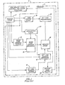
- FIGURE 1 there is shown a prior art semiconductor monolithic integrated circuit (IC) in a semiconductor body or chip 2.
- the IC 2 includes a master clock 4 whose clock cycles time the on-chip memory portion 6 of the circuit as well as other circuit portions 8 providing, for example, non-memory logic, control and other desired functions.
- the on-chip memory portion 6 includes bit line address source 10, bit line address decoders 12, word line address source 14, word line address decoders 16 and memory cell evaluation clock 20, all of the foregoing being connected to, and timed by, master clock 4.
- the decoders 12 and 16 are connected to memory cell array 22, which is connected to bit line pre-chargers 24, controlled by pre-charge clock 18.
- Memory cell evaluation clock 20 is connected to decoders 12 and 16.
- Memory output data 30 is available to non-memory circuit portions 8. It will be apparent from FIGURE 1 that all of the cyclical operations of memory 6 are synchronized with, and timed by, the clock cycle output of master clock 4 of the integrated circuit with which the memory is integrated on-chip.
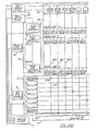
- FIGURE 2 shows additional details of portions of the memory 6 of FIGURE 1.
- the memory structure shown in FIGURE 2 includes details of the memory array 22, which has a matrix of mutually perpendicular bit lines BL0, BL1, BL2, ..., BLN and word lines WL0, WL1, WL2, ..., WLZ, at each intersection of which is provided a memory cell MC of conventional format known to the art.
- the bit lines are connected to, and served by, pre-charger cells PC0, PC1, PC2, ..., PCN, one for each bit line. All of the pre-charger cells are connected to the pre-charge clock 18.
- the pre-charger cells drive each of the bit lines to a known state, such as the high voltage level of the memory, when the precharge clock 18 is at a corresponding level (e.g., high voltage level).
- the bit lines are connected in parallel groups or sets to one or more, here shown as two, data out lines 32 and 34 respectively.
- the number of bit line groups determines the number of bits in an output word of the memory.
- Word line selection is provided by word line address decoders 16, which include decoders WLD0, WLD1, WLD2, ..., WLDZ, one for each word line, connected in parallel to the word line address source 14, the addresses typically being sequential.
- the bit line decoders are operably connected to their associated bit lines in each bit line group by sets of respective transistors CT0, CT1, ..., CT7 associated with each bit line group. Readout of memory 6 is controlled by the output of the evaluation clock 20, which is connected to all of the word line address decoders 16 and bit line address decoders 12.
- the pre-charge clock 18 output is at voltage high
- all of the word line decoders 16 are inactive and all of the word lines are at voltage low.
- the output of the pre-charge clock 18 goes low and the output evaluation clock 20 is high
- a selected one of the word line decoders as determined by the inputs from word line address source 14, fires and its word line goes from voltage low to voltage high.
- this selected word line When this selected word line goes high, it opens the gates of all of the memory cells associated with that word line to their respective bit lines. The information stored in each such memory cell is thereby made available for sensing by its associated bit line.
- the bit line address decoders 12 which are also activated when the evaluation clock 20 is high, one of the bit lines in each bit line group is selected in accordance with the bit line address inputs. The data on the selected bit lines is read out of the memory on data out lines (e.g., lines 32 and 34).
- the bit line decoders constitute an 8 to 1 multiplexer, and hence normally only one of 8 bit lines in a group is selected in a given access clock cycle.
- bit line addresses to the bit line address decoders 12 are normally sequential. Hence, in the memory of FIGURE 1 and FIGURE 2 the bit line address cycles in sequence from each to the next and on to the last bit line of each group, and then returns to the first or zero bit line of each group.
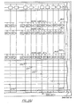
- FIGURE 3 is a timing diagram of the principal voltage signals occurring in normal operation of the memory of FIGURES 1 and 2.
- Waveforms PH1 and PH2 represent the two non-overlapping phases of the output of on-chip master clock 4 from which the memory 6 derives its timing.
- the pre-charge clock 18 is synchronized with PH1, so in every clock cycle voltage high of PH1 the bit lines are pre-charged to voltage high.
- the evaluation clock 20 is synchronous with PH2. This is evident in the timing diagram of FIGURE 3 by the pulsing to voltage high of a selected word line in synchronism with the PH2 voltage high during each clock cycle that the particular word line remains selected, and by the similarly synchronized pulsing to voltage high of the bit line decoders 12.
- bit line four BL4 is shown in FIGURE 3 to be at voltage high and BL14 at voltage low, which means that in this evaluation cycle these three memory cells contain respectively a ZERO, a ONE and a ZERO.
- evaluation at bit lines BL0, BL4 and BL14 shows in the diagram of FIGURE 3 that the memory cells contain a ONE, a ZERO and a ZERO respectively.
- evaluation shows the cells contain respectively ONE, ONE and ZERO.
- FIGURE 4 shows a memory structure similar to FIGURE 3 but embodying improvements and modifications according to the present invention.
- the output addresses from word line address source 14 are supplied to a word line address change detector 40, which monitors the word line address in each clock cycle and detects changes in word line addresses from one cycle to the next. This detection is accomplished by comparing the word line address of each given cycle with that of the next cycle.
- the output of detector 40 is connected by line 42 to pre-charge clock 18 so as to disenable pre-charging of the bit lines for all clock cycles except when a word line address change is detected.
- word line address change detector 40 may be utilized within the contemplation of the present invention.
- any suitable prior art means for storing the word line address of a given cycle and comparing it with the word line address of the next cycle may be used.
- a comparator circuit of the counter type may be used.
- one of the sample "Equality and Relative Magnitude Detection" circuits shown in the "Logic Handbook" of Digital Equipment Corporation, Copyright 1969 edition, at page 310 et seq. may be so utilized.
- address change detectors of the type shown and described in U.S. Patent 4,417,328, or in FIGURES 6 and 7 of U.S. Patent 4,514,831 may be so utilized. Both of the aforementioned patents are incorporated by reference herein.
- the present invention contemplates that detection, in each clock cycle, of no change in word line address from that of the previous cycle shall disenable the pre-charging of the bit lines for that cycle.
- detector 40 is connected by line 44 to word line address decoder 16 to sustain the activation of the decoder 16 for those clock cycles for which no word line address change is detected, thereby providing a further reduction in power consumption of the memory. Conversely, detection of a word line address change from one cycle to the next triggers the enabling of the pre-charge clock 18 output and causes pre-charging of all of the bit lines, as well as deactivation of word line decoders 16.
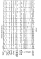
- FIGURE 5 shows a timing diagram similar to FIGURE 3, but of the improved memory of FIGURE 4 embodying and operating in accordance with the present invention. Comparing FIGURE 5 with FIGURE 3, it will be noted that the bit lines of FIGURE 5 are not pre-charged every cycle as they are in FIGURE 3. In FIGURE 5 the bit lines are pre-charged, in synchronization with PH1, only when there is a change in the word line address, thereby affording a significant reduction in power consumption of the memory of FIGURE 4.
- each given word line is activated only once in every eight cycles and remains high throughout this eight cycle period, so the power consumption involved in firing the word line decoders 16 every cycle, as is required in the memory of FIGURE 3, is thereby avoided, thus providing a further reduction in power consumption of the memory of FIGURE 4.
- bit line decoders in FIGURE 5, as in FIGURE 3 are active every cycle. But the significant reduction in bit line pre-charging, as well as frequency of word line decoder activation, provides a substantial effective reduction in power consumption for the memory of FIGURE 4 in comparison with that of FIGURE 3, without being memory cell technology dependent and without affecting operating speed.
- the present invention resides basically in selective pre-charging of the bit lines of a synchronously operated on-chip semiconductor memory only when a word line address change occurs.
- the consequent reduction in pre-charging power consumption which is a major constituent of all the power consumed by the memory, is essentially proportional to the number of bit lines per word line in each bit line group of the memory. For example, if there are eight bit lines in a data out group per word line, the power reduction factor is eight to one. It is, of course, recognized that if there are jumps, branches or other non-sequential address events which occur at addresses other than multiples of eight in such an exemplary memory, then the power reduction factor resulting from the present invention would be somewhat less, but still significant. In any event it will be apparent that the present invention affords a substantial reduction of on-chip memory power consumption in comparison with that of prior art on-chip semiconductor memories.
Landscapes
- Engineering & Computer Science (AREA)
- Microelectronics & Electronic Packaging (AREA)
- Static Random-Access Memory (AREA)
- Dram (AREA)
- Read Only Memory (AREA)
Applications Claiming Priority (1)
| Application Number | Priority Date | Filing Date | Title |
|---|---|---|---|
| US07/256,682 US4932001A (en) | 1988-10-12 | 1988-10-12 | Reducing power consumption in on-chip memory devices |
Publications (3)
| Publication Number | Publication Date |
|---|---|
| EP0366359A2 true EP0366359A2 (de) | 1990-05-02 |
| EP0366359A3 EP0366359A3 (de) | 1991-07-31 |
| EP0366359B1 EP0366359B1 (de) | 1995-07-19 |
Family
ID=22973170
Family Applications (1)
| Application Number | Title | Priority Date | Filing Date |
|---|---|---|---|
| EP89310758A Expired - Lifetime EP0366359B1 (de) | 1988-10-12 | 1989-10-19 | Leistungsverbrauchsverringerung in On-Chip-Speicheranordnungen |
Country Status (7)
| Country | Link |
|---|---|
| US (1) | US4932001A (de) |
| EP (1) | EP0366359B1 (de) |
| JP (1) | JPH02161690A (de) |
| AT (1) | ATE125383T1 (de) |
| DE (1) | DE68923529T2 (de) |
| ES (1) | ES2075057T3 (de) |
| GR (1) | GR3017377T3 (de) |
Cited By (1)
| Publication number | Priority date | Publication date | Assignee | Title |
|---|---|---|---|---|
| EP0418914A3 (en) * | 1989-09-22 | 1992-05-27 | Kabushiki Kaisha Toshiba | Semiconductor memory device |
Families Citing this family (8)
| Publication number | Priority date | Publication date | Assignee | Title |
|---|---|---|---|---|
| IT1216087B (it) * | 1988-03-15 | 1990-02-22 | Honeywell Bull Spa | Sistema di memoria con selezione predittiva di modulo. |
| JPH05234366A (ja) * | 1992-02-25 | 1993-09-10 | Mitsubishi Electric Corp | 半導体記憶装置 |
| US5592426A (en) * | 1993-10-29 | 1997-01-07 | International Business Machines Corporation | Extended segmented precharge architecture |
| US5438548A (en) * | 1993-12-10 | 1995-08-01 | Texas Instruments Incorporated | Synchronous memory with reduced power access mode |
| JPH07230691A (ja) * | 1994-02-16 | 1995-08-29 | Fujitsu Ltd | 半導体記憶装置 |
| US5430683A (en) * | 1994-03-15 | 1995-07-04 | Intel Corporation | Method and apparatus for reducing power in on-chip tag SRAM |
| US5828610A (en) * | 1997-03-31 | 1998-10-27 | Seiko Epson Corporation | Low power memory including selective precharge circuit |
| JP6142788B2 (ja) | 2013-12-04 | 2017-06-07 | 富士通株式会社 | 半導体記憶装置 |
Family Cites Families (2)
| Publication number | Priority date | Publication date | Assignee | Title |
|---|---|---|---|---|
| JPS59178685A (ja) * | 1983-03-30 | 1984-10-09 | Toshiba Corp | 半導体記憶回路 |
| US4623986A (en) * | 1984-02-23 | 1986-11-18 | Texas Instruments Incorporated | Memory access controller having cycle number register for storing the number of column address cycles in a multiple column address/single row address memory access cycle |
-
1988
- 1988-10-12 US US07/256,682 patent/US4932001A/en not_active Expired - Lifetime
-
1989
- 1989-10-11 JP JP1264832A patent/JPH02161690A/ja active Pending
- 1989-10-19 EP EP89310758A patent/EP0366359B1/de not_active Expired - Lifetime
- 1989-10-19 DE DE68923529T patent/DE68923529T2/de not_active Expired - Fee Related
- 1989-10-19 ES ES89310758T patent/ES2075057T3/es not_active Expired - Lifetime
- 1989-10-19 AT AT89310758T patent/ATE125383T1/de active
-
1995
- 1995-09-13 GR GR950402494T patent/GR3017377T3/el unknown
Cited By (1)
| Publication number | Priority date | Publication date | Assignee | Title |
|---|---|---|---|---|
| EP0418914A3 (en) * | 1989-09-22 | 1992-05-27 | Kabushiki Kaisha Toshiba | Semiconductor memory device |
Also Published As
| Publication number | Publication date |
|---|---|
| GR3017377T3 (en) | 1995-12-31 |
| ES2075057T3 (es) | 1995-10-01 |
| ATE125383T1 (de) | 1995-08-15 |
| EP0366359B1 (de) | 1995-07-19 |
| JPH02161690A (ja) | 1990-06-21 |
| DE68923529D1 (de) | 1995-08-24 |
| US4932001A (en) | 1990-06-05 |
| EP0366359A3 (de) | 1991-07-31 |
| DE68923529T2 (de) | 1996-01-04 |
Similar Documents
| Publication | Publication Date | Title |
|---|---|---|
| KR950014089B1 (ko) | 동기식 디램의 히든 셀프 리프레쉬 방법 및 장치 | |
| EP0647945B1 (de) | Burstmode-Auffrischung für DRAMs | |
| US5193072A (en) | Hidden refresh of a dynamic random access memory | |
| KR100299750B1 (ko) | 반도체 기억장치 | |
| US6343036B1 (en) | Multi-bank dynamic random access memory devices having all bank precharge capability | |
| US3940747A (en) | High density, high speed random access read-write memory | |
| EP0657891B1 (de) | Datenbusstruktur für beschleunigten Spaltenzugriff in einem RAM | |
| EP0145488B1 (de) | Halbleiterspeicheranordnung | |
| EP0165106A2 (de) | Halbleiterspeichergerät | |
| US4636987A (en) | Semiconductor dynamic memory device with multiplexed sense amplifier and write-activated active loads | |
| US4638462A (en) | Self-timed precharge circuit | |
| US4112513A (en) | Method for refreshing storage contents of MOS memories | |
| EP0326183B1 (de) | Pseudo-statischer Direktzugriffspeicher | |
| US4932001A (en) | Reducing power consumption in on-chip memory devices | |
| KR100290286B1 (ko) | 빠른 입출력 라인 프리차지 스킴을 구비한 반도체 메모리 장치 | |
| US5185719A (en) | High speed dynamic, random access memory with extended reset/precharge time | |
| US5305283A (en) | Dram column address latching technique | |
| US6172925B1 (en) | Memory array bitline timing circuit | |
| US5619464A (en) | High performance RAM array circuit employing self-time clock generator for enabling array accessess | |
| US4656613A (en) | Semiconductor dynamic memory device with decoded active loads | |
| JPH0887887A (ja) | 半導体記憶装置 | |
| EP0208316B1 (de) | Dynamische Speicheranordnung | |
| EP0239916A2 (de) | Halbleiterspeichervorrichtung mit einem Testmodus und einem Standardmodusbetrieb | |
| US6466470B1 (en) | Circuitry and method for resetting memory without a write cycle | |
| US5305274A (en) | Method and apparatus for refreshing a dynamic random access memory |
Legal Events
| Date | Code | Title | Description |
|---|---|---|---|
| PUAI | Public reference made under article 153(3) epc to a published international application that has entered the european phase |
Free format text: ORIGINAL CODE: 0009012 |
|
| AK | Designated contracting states |
Kind code of ref document: A2 Designated state(s): AT BE CH DE ES FR GB GR IT LI LU NL SE |
|
| PUAL | Search report despatched |
Free format text: ORIGINAL CODE: 0009013 |
|
| AK | Designated contracting states |
Kind code of ref document: A3 Designated state(s): AT BE CH DE ES FR GB GR IT LI LU NL SE |
|
| 17P | Request for examination filed |
Effective date: 19920109 |
|
| 17Q | First examination report despatched |
Effective date: 19940516 |
|
| GRAA | (expected) grant |
Free format text: ORIGINAL CODE: 0009210 |
|
| AK | Designated contracting states |
Kind code of ref document: B1 Designated state(s): AT BE CH DE ES FR GB GR IT LI LU NL SE |
|
| REF | Corresponds to: |
Ref document number: 125383 Country of ref document: AT Date of ref document: 19950815 Kind code of ref document: T |
|
| REF | Corresponds to: |
Ref document number: 68923529 Country of ref document: DE Date of ref document: 19950824 |
|
| ITF | It: translation for a ep patent filed | ||
| REG | Reference to a national code |
Ref country code: ES Ref legal event code: FG2A Ref document number: 2075057 Country of ref document: ES Kind code of ref document: T3 |
|
| ET | Fr: translation filed | ||
| REG | Reference to a national code |
Ref country code: GR Ref legal event code: FG4A Free format text: 3017377 |
|
| PLBE | No opposition filed within time limit |
Free format text: ORIGINAL CODE: 0009261 |
|
| STAA | Information on the status of an ep patent application or granted ep patent |
Free format text: STATUS: NO OPPOSITION FILED WITHIN TIME LIMIT |
|
| 26N | No opposition filed | ||
| PGFP | Annual fee paid to national office [announced via postgrant information from national office to epo] |
Ref country code: AT Payment date: 19970918 Year of fee payment: 9 |
|
| PGFP | Annual fee paid to national office [announced via postgrant information from national office to epo] |
Ref country code: SE Payment date: 19971006 Year of fee payment: 9 |
|
| PGFP | Annual fee paid to national office [announced via postgrant information from national office to epo] |
Ref country code: GR Payment date: 19971015 Year of fee payment: 9 |
|
| PGFP | Annual fee paid to national office [announced via postgrant information from national office to epo] |
Ref country code: BE Payment date: 19971105 Year of fee payment: 9 |
|
| PGFP | Annual fee paid to national office [announced via postgrant information from national office to epo] |
Ref country code: CH Payment date: 19980109 Year of fee payment: 9 |
|
| PGFP | Annual fee paid to national office [announced via postgrant information from national office to epo] |
Ref country code: LU Payment date: 19980306 Year of fee payment: 9 |
|
| PG25 | Lapsed in a contracting state [announced via postgrant information from national office to epo] |
Ref country code: LU Free format text: LAPSE BECAUSE OF NON-PAYMENT OF DUE FEES Effective date: 19981019 Ref country code: AT Free format text: LAPSE BECAUSE OF NON-PAYMENT OF DUE FEES Effective date: 19981019 |
|
| PG25 | Lapsed in a contracting state [announced via postgrant information from national office to epo] |
Ref country code: SE Free format text: LAPSE BECAUSE OF NON-PAYMENT OF DUE FEES Effective date: 19981020 |
|
| PG25 | Lapsed in a contracting state [announced via postgrant information from national office to epo] |
Ref country code: LI Free format text: LAPSE BECAUSE OF NON-PAYMENT OF DUE FEES Effective date: 19981031 Ref country code: GR Free format text: LAPSE BECAUSE OF NON-PAYMENT OF DUE FEES Effective date: 19981031 Ref country code: CH Free format text: LAPSE BECAUSE OF NON-PAYMENT OF DUE FEES Effective date: 19981031 Ref country code: BE Free format text: LAPSE BECAUSE OF NON-PAYMENT OF DUE FEES Effective date: 19981031 |
|
| BERE | Be: lapsed |
Owner name: ADVANCED MICRO DEVICES INC. Effective date: 19981031 |
|
| REG | Reference to a national code |
Ref country code: CH Ref legal event code: PL |
|
| EUG | Se: european patent has lapsed |
Ref document number: 89310758.1 |
|
| PGFP | Annual fee paid to national office [announced via postgrant information from national office to epo] |
Ref country code: ES Payment date: 19991014 Year of fee payment: 11 |
|
| PG25 | Lapsed in a contracting state [announced via postgrant information from national office to epo] |
Ref country code: ES Free format text: LAPSE BECAUSE OF NON-PAYMENT OF DUE FEES Effective date: 20001020 |
|
| REG | Reference to a national code |
Ref country code: GB Ref legal event code: IF02 |
|
| PGFP | Annual fee paid to national office [announced via postgrant information from national office to epo] |
Ref country code: GB Payment date: 20020913 Year of fee payment: 14 |
|
| PGFP | Annual fee paid to national office [announced via postgrant information from national office to epo] |
Ref country code: NL Payment date: 20020919 Year of fee payment: 14 |
|
| PGFP | Annual fee paid to national office [announced via postgrant information from national office to epo] |
Ref country code: FR Payment date: 20021003 Year of fee payment: 14 |
|
| PGFP | Annual fee paid to national office [announced via postgrant information from national office to epo] |
Ref country code: DE Payment date: 20021031 Year of fee payment: 14 |
|
| PG25 | Lapsed in a contracting state [announced via postgrant information from national office to epo] |
Ref country code: GB Free format text: LAPSE BECAUSE OF NON-PAYMENT OF DUE FEES Effective date: 20031019 |
|
| REG | Reference to a national code |
Ref country code: ES Ref legal event code: FD2A Effective date: 20011113 |
|
| PG25 | Lapsed in a contracting state [announced via postgrant information from national office to epo] |
Ref country code: NL Free format text: LAPSE BECAUSE OF NON-PAYMENT OF DUE FEES Effective date: 20040501 Ref country code: DE Free format text: LAPSE BECAUSE OF NON-PAYMENT OF DUE FEES Effective date: 20040501 |
|
| GBPC | Gb: european patent ceased through non-payment of renewal fee |
Effective date: 20031019 |
|
| PG25 | Lapsed in a contracting state [announced via postgrant information from national office to epo] |
Ref country code: FR Free format text: LAPSE BECAUSE OF NON-PAYMENT OF DUE FEES Effective date: 20040630 |
|
| NLV4 | Nl: lapsed or anulled due to non-payment of the annual fee |
Effective date: 20040501 |
|
| REG | Reference to a national code |
Ref country code: FR Ref legal event code: ST |
|
| PG25 | Lapsed in a contracting state [announced via postgrant information from national office to epo] |
Ref country code: IT Free format text: LAPSE BECAUSE OF NON-PAYMENT OF DUE FEES Effective date: 20051019 |