EP0366294B1 - TTL-ECL-Pegelumsetzungsschaltung - Google Patents
TTL-ECL-Pegelumsetzungsschaltung Download PDFInfo
- Publication number
- EP0366294B1 EP0366294B1 EP89310266A EP89310266A EP0366294B1 EP 0366294 B1 EP0366294 B1 EP 0366294B1 EP 89310266 A EP89310266 A EP 89310266A EP 89310266 A EP89310266 A EP 89310266A EP 0366294 B1 EP0366294 B1 EP 0366294B1
- Authority
- EP
- European Patent Office
- Prior art keywords
- connection node
- diode
- transistor
- resistor
- circuit
- Prior art date
- Legal status (The legal status is an assumption and is not a legal conclusion. Google has not performed a legal analysis and makes no representation as to the accuracy of the status listed.)
- Expired - Lifetime
Links
Images


Classifications
-
- H—ELECTRICITY
- H03—ELECTRONIC CIRCUITRY
- H03K—PULSE TECHNIQUE
- H03K19/00—Logic circuits, i.e. having at least two inputs acting on one output; Inverting circuits
- H03K19/0175—Coupling arrangements; Interface arrangements
- H03K19/018—Coupling arrangements; Interface arrangements using bipolar transistors only
- H03K19/01806—Interface arrangements
-
- H—ELECTRICITY
- H03—ELECTRONIC CIRCUITRY
- H03K—PULSE TECHNIQUE
- H03K19/00—Logic circuits, i.e. having at least two inputs acting on one output; Inverting circuits
- H03K19/003—Modifications for increasing the reliability for protection
- H03K19/00346—Modifications for eliminating interference or parasitic voltages or currents
- H03K19/00353—Modifications for eliminating interference or parasitic voltages or currents in bipolar transistor circuits
-
- H—ELECTRICITY
- H03—ELECTRONIC CIRCUITRY
- H03K—PULSE TECHNIQUE
- H03K19/00—Logic circuits, i.e. having at least two inputs acting on one output; Inverting circuits
- H03K19/003—Modifications for increasing the reliability for protection
- H03K19/00369—Modifications for compensating variations of temperature, supply voltage or other physical parameters
- H03K19/00376—Modifications for compensating variations of temperature, supply voltage or other physical parameters in bipolar transistor circuits
Definitions
- the present invention relates to a TTL-ECL converting circuit, and more specifically to a TTL-ECL converting circuit which operates at a high speed and which is free from self-oscillation.
- ECL emitter coupled logic circuits in the form of an integrated circuit having a high integration density
- main-frames communication instruments
- LSI testers measuring instruments
- TTL transistor-transistor logic
- TTL-ECL circuit comprises a diode having a cathode connected to an input terminal for a TTL signal and an anode connected to a first connection terminal, a resistor having its one end connected to a high voltage supply line and its other end connected to said first connection node, a transistor having a collector connected to said high voltage supply line, a base connected to said first connection node and an emitter connected to a second connection node, a level shift means having its one end connected to said second connection node and its other end connected to a third connection node, a constant current source having its one end connected to said third connection node and its other end connected to a low voltage supply line, and an emitter follower connected between an intermediate voltage supply line and said low voltage supply line and having an input coupled to said third connection node and an output connected to an output terminal for an
- the present inventor has appreciated that the conventional TTL-ECL level converting circuits have been disadvantageous in that the base potential of a transistor receiving a TTL input signal is apt to cause self-oscillation, and the fluctuating voltage is propagated as noise to an ECL level output signal.
- the noise has the possibility of causing the next ECL circuit stage to malfunction.
- the conventional TTL-ECL level converting circuits have a logical amplitude of the ECL output signal much larger than the logical amplitude in ordinary ECL circuits. Therefore, the propagation delay time is inevitably large.
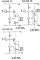
- FIG. 1 there is shown a circuit diagram of a proposed TTL-ECL level converting circuit.
- the circuit illustrated includes an input terminal IN for receiving a TTL level signal and an output terminal OUT for outputting an ECL level signal.
- the input terminal IN is connected to the cathode of a Schottky barrier diode D 1 , whose anode is connected to one end of a resistor R 1 , to the base of a first transistor Q 1 and to the collector of a second transistor Q 2 , respectively.
- the other end of the resistor R 1 and the collector of the first transistor Q 1 are connected to a high voltage supply line V CC .
- the emitter of the first transistor Q 1 is connected to a low voltage supply line V EE through a diode D 21 , a resistor R 31 and a constant current source Ics.
- the emitter of the second transistor Q 2 is connected to a ground line GND, and the base of the second transistor Q 2 is connected through a resistor R 21 to a connection node between the diode D 21 and the resistor R 31 .
- Another Schottky barrier diode D 31 is connected between the ground line GND and the connection node between the diode D 21 and the resistor R 31 .
- a third transistor Q 3 having its collector connected to the ground line GND, and its base connected to a connection node between the resistor R 31 and the constant current source Ics.
- the emitter of the third transistor Q 3 is connected through a resistor R 4 to the low voltage supply line V EE and is also connected to the output terminal OUT.
- a TTL level signal applied to the input terminal IN is level-shifted by the diode D 1 , the transistor Q 1 , the diode D 21 and the resistor R 31 , and outputted as an ECL level signal from the output terminal OUT through an emitter follower formed of the transistor Q 3 and the resistor R 4 .
- the ECL level signal is set as follows: When the TTL level signal of a high level V IH is inputted, the transistor Q 1 , the diode D 21 and the transistor Q 2 are brought into the on condition, and on the other hand, the diode D 1 is brought into the off condition. If a forward direction voltage of diodes and transistors is expressed by V F , this input voltage V IH must fulfil the following condition (1) in order to render the diode D 1 off: V IH ⁇ V F (Q 2 ) + V F (D 21 ) + V F (Q 1 ) - V F (D 1 )
- V F V F (Q 2 ) - R 31 ⁇ Ics - V F (Q 3 ) ⁇ - R 31 ⁇ Ics
- Ics the current value of the constant current source Ics
- V IL V IL ⁇ -V F (D 31 ) + V F (D 21 ) + V F (Q 1 ) - V F (D 1 )
- the low level condition becomes stable under the condition of V IL ⁇ 0.8V.
- V OL -V F (D 31 ) - R 31 ⁇ Ics - V F (Q 3 )
- the ECL level output of the circuit shown in Figure 1 has a logical amplitude (a difference between V OH and V OL ) corresponding to the sum of the forward direction operating voltage of one transistor and the forward direction operating voltage of one Schottky barrier diode (about 1.2V).
- the present inventor has appreciated that a propagation delay will occur in the course of the level shifting, and therefore, the base potential of the transistor Q 1 is apt to cause oscillation due to a delay of the turning-on of the transistor Q 2 and a voltage drop caused across the resistor R 1 by an abruptly increasing operation current.
- the base potential of the transistor Q 1 elevates towards the potential of the high voltage supply V CC through the resistor R 1 .
- This elevated voltage is propagated to the base of the transistor Q 2 through the transistor Q 1 , the diode D 21 and the resistor R 21 with a delay corresponding to the propagation delay time of these elements.
- the current of the transistor Q 2 is increased, and the collector potential of the transistor Q 2 is correspondingly decreased due to the voltage drop across the resistor R 1 .
- the drop of the collector potential of the transistor Q 2 is propagated to the base of the transistor Q 2 after a constant delay time, so that the base potential of the transistor Q 2 is decreased, and therefore, the collector current of the transistor Q 2 is correspondingly decreased. As result, the collector potential of the transistor Q 2 is elevated at this time.
- the logical amplitude of the ECL output signal corresponds to the sum of the forward direction operating voltage of one transistor Q 2 and the forward direction operating voltage of one Schottky barrier diode D 31 .
- This logical amplitude of the ECL output signal is much larger than a logical amplitude of 0.6V in ordinary ECL circuits. Therefore, the propagation delay time inevitably becomes large.
- FIG 2 there is shown the circuit diagram of one embodiment of the TTL-ECL level converting circuit in accordance with the present invention.
- elements similar or corresponding to those shown in Figure 1 are given the same reference characters, and explanation thereof will be omitted for simplification of description.
- a level shift circuit in the conversion circuit shown Figure 2 connected to the emitter of the transistor Q 1 is composed of a series circuit consisting of a resistor R 3 and a diode D 2 in such a manner that the resistor R 3 is connected at its one end to the emitter of the transistor Q 1 and at its other end to the anode of the diode D 2 , and the cathode of the diode D 2 is connected to the current source Ics.
- a connection node between the resistor R 3 and the diode D 2 is connected directly to the base of the transistor Q 2 .
- a resistor R 2 is connected between the emitter of the transistor Q 2 and the ground line GND.
- the cathode of an anode-grounded diode D 3 for low level clamping is connected to the cathode of the diode D 2 which forms an output end of the level shift circuit.
- the operation of the TTL-ECL level converting circuit shown in Figure 2 will now be explained.
- the TTL level input signal is at a high level V IH
- the transistors Q 1 and Q 2 and the diode D 2 are brought into the on condition, and, on the other hand, the diodes D 1 and D 3 are brought into the off condition.
- the operation current of the transistor Q 2 flows through the resistor R 1 so that an anode potential of the diode D 1 is maintained at a constant level.
- the voltage difference V(D 1 ) between the anode potential of the diode D 1 and the high level TTL level signal applied at the cathode of the diode D 1 becomes smaller than the forward direction operation voltage V F (D 1 ) of the diode D 1 , and therefore, the diode D 1 is turned off. With this, the status is balanced.
- V(D 1 ) V F (Q 1 ) + R 3 ⁇ Ics + V F (Q 2 ) + R 2 ⁇ I F (Q 2 ) - V IH
- R 3 2K ⁇
- Ics 0.3mA
- R 2 1K ⁇
- V CC 5V
- R 1 20K ⁇
- V F (D 1 ) 0.4V
- V OH R 2 ⁇ I F (Q 2 ) + V F (Q 2 ) - V F (D 2 ) - V F (Q 3 ) ⁇ R 2 ⁇ I F (Q 2 ) - V F (Q 3 )
- V IL ⁇ 0.8V
- V F (D 1 ) 0.4V
- R 3 2K ⁇
- Ics 0.3mA
- V OL - V F (D 3 ) - V F (Q 3 )
- the logical amplitude of the ECL level output signal of the converting circuit shown in Figure 2 is about 0.93V, which is apparently smaller than that of the circuit shown in Figure 1.
- the logical amplitude of the ECL level output signal can be reduced to 0.6V under the condition that the equations (6a) and (8) are fulfilled.
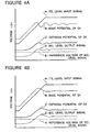
- Figure 4A shows a graph illustrating voltage variations on various points in the converting circuit shown in Figure 2 in which the resistor R 2 is removed and the emitter of the transistor Q 2 is directly connected to the ground line GND.
- Figure 4B is a graph illustrating voltage variations on various points in the converting circuit shown in Figure 2. These figures show transitions when the TTL input signal is brought from the low level to the high level. In each of these figures, the line A shows the TTL level input signal, and the line B shows the base potential of the transistor Q 1 .
- the lines C, D and E indicate the cathode potential of the diode D 2 , the ECL level output signal, and a reference voltage for the ECL level signal, respectively.
- the values of the respective elements used in the circuit for the simulation is in accordance with the values as mentioned hereinbefore.
- the level shift circuit is composed of a series circuit consisting of two diodes D 21 and D 2 .
- the level shift circuit is composed of a low impedance circuit formed of only the diodes, the propagation delay can be shortened to a minimum extent.
- the level shift circuit is composed of a series circuit consisting of two resistors R 3 and R 32 .
- the constant current flows through the resistors of the level shift circuit, temperature dependency of the threshold of the converting circuit is eliminated.
- the forward direction operating voltage of diodes and transistors has a temperature dependency of about 2mV/°C.
- the temperature dependencies of the Schottky barrier diode D 1 and the transistors Q 1 are countervailed or compensated to each other.
- the level shift circuit does not have a temperature dependency.
- the converting circuit modified in accordance with the modification shown in Figure 3B has a threshold with no temperature dependency. This is very advantageous in that even if the converting circuit and an ECL circuit which generates a large amount of heat due to power consumption are integrated in the same chip, the converting circuit maintains its threshold at a constant level regardless of temperature change.
- the level shift circuit is composed of a series circuit consisting of a diode D 21 and a resistor R 32 in such a manner that the diode D 21 is connected at its anode to the emitter of the transistor D 21 and at its cathode to one end of the resistor R 32 and the base of the transistor Q 2 .
- This modified converting circuit has an excellent balance concerning both the delay time and the threshold temperature dependency.
Landscapes
- Engineering & Computer Science (AREA)
- Computer Hardware Design (AREA)
- Physics & Mathematics (AREA)
- Computing Systems (AREA)
- General Engineering & Computer Science (AREA)
- Mathematical Physics (AREA)
- Logic Circuits (AREA)
Claims (6)
- TTL-ECL-Pegelumsetzungsschaltung mit einer Schottky-Diode (D1), deren Katode mit einem Eingangsanschluß (IN) für ein TTL-Signal und deren Anode mit einem ersten Verbindungsknoten verbunden ist, einem Widerstand (R1), dessen eines Ende mit einer Versorgungsleitung mit hoher Spannung (VCC) und dessen anderes Ende mit dem ersten Verbindungsknoten verbunden ist, einem ersten Transistor (Q1), dessen Kollektor mit der Versorgungsleitung mit hoher Spannung verbunden ist, dessen Basis mit dem ersten Verbindungsknoten und dessen Emitter mit einem zweiten Verbindungsknoten verbunden ist, einer Pegelverschiebungseinrichtung (R3, D2; D21, D2; R3, R32; D21, R32), deren eines Ende mit dem zweiten Verbindungsknoten verbunden ist, wobei ein Zwischenknoten einen dritten Verbindungsknoten bildet, und deren anderes Ende mit einem vierten Verbindungsknoten verbunden ist, einer Konstantstromquelle (ICS), deren eines Ende mit dem vierten Verbindungsknoten und deren anderes Ende mit einer Versorgungsleitung mit niedriger Spannung (VEE) verbunden ist, einem zweiten Transistor (Q2), dessen Kollektor mit dem ersten Verbindungsknoten, dessen Basis mit dem dritten Verbindungsknoten und dessen Emitter über einen zweiten Widerstand (R2) mit einer Versorgungsleitung mit Zwischenspannung (GND) verbunden ist, und einem Emitterfolger (Q3, R4), der zwischen die Versorgungsleitung mit Zwischenspannung und die Versorgungsleitung mit niedriger Spannung geschaltet ist, dessen Eingang mit dem vierten Verbindungsknoten und dessen Ausgang mit einem Ausgangsanschluß (OUT) für ein ECL-Signal verbunden ist.
- Schaltung nach Anspruch 1, ferner mit einer Diode (D3), deren Anode mit der Versorgungsleitung mit Zwischenspannung und deren Katode mit dem vierten Verbindungsknoten verbunden ist.
- Schaltung nach Anspruch 1 oder 2, wobei die Pegelverschiebungseinrichtung einen Widerstand (R3), dessen eines Ende mit dem zweiten Verbindungsknoten und dessen anderes Ende mit dem dritten Verbindungsknoten verbunden ist, und eine Diode (D2), deren Anode mit dem dritten Verbindungsknoten und deren Katode mit dem vierten Verbindungsknoten verbunden ist, aufweist.
- Schaltung nach Anspruch 1 oder 2, wobei die Pegelverschiebungseinrichtung eine Diode (D21), deren Anode mit dem zweiten Verbindungsknoten und deren Katode mit dem dritten Verbindungsknoten verbunden ist, und eine andere Diode (D2), deren Anode mit dem dritten Verbindungsknoten und deren Katode mit dem vierten Verbindungsknoten verbunden ist, aufweist.
- Schaltung nach Anspruch 1 oder 2, wobei die Pegelverschiebungseinrichtung einen Widerstand (R3), dessen eines Ende mit dem zweiten Verbindungsknoten und dessen anderes Ende mit dem dritten Verbindungsknoten verbunden ist, und einen anderen Widerstand (R32), dessen eines Ende mit dem dritten Verbindungsknoten und dessen anderes Ende mit dem vierten Verbindungsknoten verbunden ist, aufweist.
- Schaltung nach Anspruch 1 oder 2, wobei die Pegelverschiebungseinrichtung eine Diode (D21), deren Anode mit dem zweiten Verbindungsknoten und deren Katode mit dem dritten Verbindungsknoten verbunden ist, und einen Widerstand (R32), dessen eines Ende mit dem dritten Verbindungsknoten und dessen anderes Ende mit dem vierten Verbindungsknoten verbunden ist, aufweist.
Applications Claiming Priority (2)
| Application Number | Priority Date | Filing Date | Title |
|---|---|---|---|
| JP63252682A JPH0716154B2 (ja) | 1988-10-06 | 1988-10-06 | Ttl−eclレベル変換回路 |
| JP252682/88 | 1988-10-06 |
Publications (3)
| Publication Number | Publication Date |
|---|---|
| EP0366294A2 EP0366294A2 (de) | 1990-05-02 |
| EP0366294A3 EP0366294A3 (de) | 1990-12-05 |
| EP0366294B1 true EP0366294B1 (de) | 1997-07-02 |
Family
ID=17240776
Family Applications (1)
| Application Number | Title | Priority Date | Filing Date |
|---|---|---|---|
| EP89310266A Expired - Lifetime EP0366294B1 (de) | 1988-10-06 | 1989-10-06 | TTL-ECL-Pegelumsetzungsschaltung |
Country Status (4)
| Country | Link |
|---|---|
| US (1) | US5036225A (de) |
| EP (1) | EP0366294B1 (de) |
| JP (1) | JPH0716154B2 (de) |
| DE (1) | DE68928145T2 (de) |
Families Citing this family (4)
| Publication number | Priority date | Publication date | Assignee | Title |
|---|---|---|---|---|
| JPH03222516A (ja) * | 1990-01-29 | 1991-10-01 | Fujitsu Ltd | 半導体装置 |
| JPH06188718A (ja) * | 1992-12-15 | 1994-07-08 | Mitsubishi Electric Corp | 半導体集積回路装置 |
| US5920729A (en) * | 1996-04-30 | 1999-07-06 | Vtc Inc. | Apparatus for providing pair of complementary outputs with first and subcircuits to convert non-complementary and complementary inputs to first and second pair of complementary output |
| CN104821818A (zh) * | 2015-05-27 | 2015-08-05 | 沈震强 | 提高光耦输出速度的方法 |
Family Cites Families (7)
| Publication number | Priority date | Publication date | Assignee | Title |
|---|---|---|---|---|
| DE3006176C2 (de) * | 1980-02-19 | 1981-12-03 | Siemens AG, 1000 Berlin und 8000 München | Einrichtung zur Signalpegelverschiebung |
| FR2534752A1 (fr) * | 1982-10-18 | 1984-04-20 | Radiotechnique Compelec | Circuit convertisseur de niveaux de signaux entre une logique de type saturee et une logique de type non saturee |
| US4654549A (en) * | 1985-06-04 | 1987-03-31 | Fairchild Semiconductor Corporation | Transistor-transistor logic to emitter coupled logic translator |
| JPH0763139B2 (ja) * | 1985-10-31 | 1995-07-05 | 日本電気株式会社 | レベル変換回路 |
| US4771191A (en) * | 1987-02-03 | 1988-09-13 | Julio Estrada | TTL to ECL translator |
| JPS63302621A (ja) * | 1987-06-02 | 1988-12-09 | Fujitsu Ltd | 半導体集積回路 |
| US4825108A (en) * | 1987-06-15 | 1989-04-25 | North American Philips Corporation, Signetics Division | Voltage translator with restricted output voltage swing |
-
1988
- 1988-10-06 JP JP63252682A patent/JPH0716154B2/ja not_active Expired - Lifetime
-
1989
- 1989-10-06 US US07/417,973 patent/US5036225A/en not_active Expired - Fee Related
- 1989-10-06 DE DE68928145T patent/DE68928145T2/de not_active Expired - Fee Related
- 1989-10-06 EP EP89310266A patent/EP0366294B1/de not_active Expired - Lifetime
Non-Patent Citations (3)
| Title |
|---|
| E. KÜHN "Handbuch TTL- und CMOS- Schaltkreise" 1985, VEB VERLAG TECHNIK, Berlin, pages 317, 320 * |
| M. HERPY "Analoge Integrierte Schaltungen" 1979, FRANZIS-VERLAG, München, page 251 * |
| TURINSKY: "Pegelwandlung ECL-TTL und umgekehrt" * |
Also Published As
| Publication number | Publication date |
|---|---|
| DE68928145T2 (de) | 1998-02-19 |
| EP0366294A3 (de) | 1990-12-05 |
| JPH0716154B2 (ja) | 1995-02-22 |
| JPH02100418A (ja) | 1990-04-12 |
| DE68928145D1 (de) | 1997-08-07 |
| EP0366294A2 (de) | 1990-05-02 |
| US5036225A (en) | 1991-07-30 |
Similar Documents
| Publication | Publication Date | Title |
|---|---|---|
| US4628216A (en) | Merging of logic function circuits to ECL latch or flip-flop circuit | |
| US4791323A (en) | Level translation circuit | |
| US5365127A (en) | Circuit for conversion from CMOS voltage levels to shifted ECL voltage levels with process compensation | |
| US4810908A (en) | Semiconductor logic circuit comprising clock driver and clocked logic circuit | |
| KR890004886B1 (ko) | 래치회로 | |
| US4779009A (en) | Master-slave type flip-flop circuit | |
| US4410816A (en) | ECL Integrated circuit | |
| US5214317A (en) | CMOS to ECL translator with incorporated latch | |
| JPH0356017B2 (de) | ||
| EP0366294B1 (de) | TTL-ECL-Pegelumsetzungsschaltung | |
| KR900004591B1 (ko) | 입력회로 | |
| EP0396486A1 (de) | Empfänger- und Spannungspegelkonverter-Schaltkreis | |
| KR0138949B1 (ko) | 씨모스 회로와 바이폴라 회로가 혼재되어 있는 반도체 디바이스 | |
| US5159208A (en) | Interface circuit provided between a compound semiconductor logic circuit and a bipolar transistor circuit | |
| EP0326996A2 (de) | Integrierte Halbleiterschaltung mit einer Pegelumsetzungsschaltung | |
| US5248909A (en) | ECL-TO-GaAs level converting circuit | |
| EP0765036A2 (de) | Pegel-Konverterschaltung zum Umsetzen von Eingangspegeln in ECL-Pegel unabhängig von Variationen der Speisespannung | |
| EP0433685B1 (de) | Integrierte Halbleiterschaltung mit ECL-Schaltungen | |
| JP2580250B2 (ja) | バイポーラcmosレベル変換回路 | |
| EP0168230B1 (de) | Multiplexier-Dekodier-Schaltungseinheit | |
| US5233239A (en) | ECL circuit with feedback circuitry for increased speed | |
| EP0304576A2 (de) | Oszillator für Toranordnung mit Rauschunterdrückung | |
| US5065051A (en) | Ecl-ttl level converting circuit | |
| US4942320A (en) | Transistor circuit with improved α ray resistant properties | |
| KR940003806B1 (ko) | ECL-GaAs 레벨 변환 회로 |
Legal Events
| Date | Code | Title | Description |
|---|---|---|---|
| PUAI | Public reference made under article 153(3) epc to a published international application that has entered the european phase |
Free format text: ORIGINAL CODE: 0009012 |
|
| 17P | Request for examination filed |
Effective date: 19891025 |
|
| AK | Designated contracting states |
Kind code of ref document: A2 Designated state(s): DE FR GB |
|
| PUAL | Search report despatched |
Free format text: ORIGINAL CODE: 0009013 |
|
| AK | Designated contracting states |
Kind code of ref document: A3 Designated state(s): DE FR GB |
|
| 17Q | First examination report despatched |
Effective date: 19920930 |
|
| APAB | Appeal dossier modified |
Free format text: ORIGINAL CODE: EPIDOS NOAPE |
|
| GRAG | Despatch of communication of intention to grant |
Free format text: ORIGINAL CODE: EPIDOS AGRA |
|
| GRAH | Despatch of communication of intention to grant a patent |
Free format text: ORIGINAL CODE: EPIDOS IGRA |
|
| GRAH | Despatch of communication of intention to grant a patent |
Free format text: ORIGINAL CODE: EPIDOS IGRA |
|
| GRAA | (expected) grant |
Free format text: ORIGINAL CODE: 0009210 |
|
| AK | Designated contracting states |
Kind code of ref document: B1 Designated state(s): DE FR GB |
|
| REF | Corresponds to: |
Ref document number: 68928145 Country of ref document: DE Date of ref document: 19970807 |
|
| ET | Fr: translation filed | ||
| PLBE | No opposition filed within time limit |
Free format text: ORIGINAL CODE: 0009261 |
|
| STAA | Information on the status of an ep patent application or granted ep patent |
Free format text: STATUS: NO OPPOSITION FILED WITHIN TIME LIMIT |
|
| 26N | No opposition filed | ||
| PGFP | Annual fee paid to national office [announced via postgrant information from national office to epo] |
Ref country code: GB Payment date: 19981009 Year of fee payment: 10 |
|
| PGFP | Annual fee paid to national office [announced via postgrant information from national office to epo] |
Ref country code: FR Payment date: 19981030 Year of fee payment: 10 |
|
| PGFP | Annual fee paid to national office [announced via postgrant information from national office to epo] |
Ref country code: DE Payment date: 19981229 Year of fee payment: 10 |
|
| PG25 | Lapsed in a contracting state [announced via postgrant information from national office to epo] |
Ref country code: GB Free format text: LAPSE BECAUSE OF NON-PAYMENT OF DUE FEES Effective date: 19991006 |
|
| GBPC | Gb: european patent ceased through non-payment of renewal fee |
Effective date: 19991006 |
|
| PG25 | Lapsed in a contracting state [announced via postgrant information from national office to epo] |
Ref country code: FR Free format text: LAPSE BECAUSE OF NON-PAYMENT OF DUE FEES Effective date: 20000630 |
|
| PG25 | Lapsed in a contracting state [announced via postgrant information from national office to epo] |
Ref country code: DE Free format text: LAPSE BECAUSE OF NON-PAYMENT OF DUE FEES Effective date: 20000801 |
|
| REG | Reference to a national code |
Ref country code: FR Ref legal event code: ST |
|
| APAH | Appeal reference modified |
Free format text: ORIGINAL CODE: EPIDOSCREFNO |