EP0364224A1 - Procédé pour fabriquer des informations optiques et appareil ayant un système empêchant une déficience durant le guidage de piste - Google Patents
Procédé pour fabriquer des informations optiques et appareil ayant un système empêchant une déficience durant le guidage de piste Download PDFInfo
- Publication number
- EP0364224A1 EP0364224A1 EP89310371A EP89310371A EP0364224A1 EP 0364224 A1 EP0364224 A1 EP 0364224A1 EP 89310371 A EP89310371 A EP 89310371A EP 89310371 A EP89310371 A EP 89310371A EP 0364224 A1 EP0364224 A1 EP 0364224A1
- Authority
- EP
- European Patent Office
- Prior art keywords
- error signal
- tracking
- light beam
- tracking error
- time
- Prior art date
- Legal status (The legal status is an assumption and is not a legal conclusion. Google has not performed a legal analysis and makes no representation as to the accuracy of the status listed.)
- Granted
Links
Images


Classifications
-
- G—PHYSICS
- G11—INFORMATION STORAGE
- G11B—INFORMATION STORAGE BASED ON RELATIVE MOVEMENT BETWEEN RECORD CARRIER AND TRANSDUCER
- G11B11/00—Recording on or reproducing from the same record carrier wherein for these two operations the methods are covered by different main groups of groups G11B3/00 - G11B7/00 or by different subgroups of group G11B9/00; Record carriers therefor
- G11B11/10—Recording on or reproducing from the same record carrier wherein for these two operations the methods are covered by different main groups of groups G11B3/00 - G11B7/00 or by different subgroups of group G11B9/00; Record carriers therefor using recording by magnetic means or other means for magnetisation or demagnetisation of a record carrier, e.g. light induced spin magnetisation; Demagnetisation by thermal or stress means in the presence or not of an orienting magnetic field
- G11B11/105—Recording on or reproducing from the same record carrier wherein for these two operations the methods are covered by different main groups of groups G11B3/00 - G11B7/00 or by different subgroups of group G11B9/00; Record carriers therefor using recording by magnetic means or other means for magnetisation or demagnetisation of a record carrier, e.g. light induced spin magnetisation; Demagnetisation by thermal or stress means in the presence or not of an orienting magnetic field using a beam of light or a magnetic field for recording by change of magnetisation and a beam of light for reproducing, i.e. magneto-optical, e.g. light-induced thermomagnetic recording, spin magnetisation recording, Kerr or Faraday effect reproducing
- G11B11/1055—Disposition or mounting of transducers relative to record carriers
- G11B11/10556—Disposition or mounting of transducers relative to record carriers with provision for moving or switching or masking the transducers in or out of their operative position
-
- G—PHYSICS
- G11—INFORMATION STORAGE
- G11B—INFORMATION STORAGE BASED ON RELATIVE MOVEMENT BETWEEN RECORD CARRIER AND TRANSDUCER
- G11B7/00—Recording or reproducing by optical means, e.g. recording using a thermal beam of optical radiation by modifying optical properties or the physical structure, reproducing using an optical beam at lower power by sensing optical properties; Record carriers therefor
- G11B7/002—Recording, reproducing or erasing systems characterised by the shape or form of the carrier
- G11B7/0025—Recording, reproducing or erasing systems characterised by the shape or form of the carrier with cylinders or cylinder-like carriers or cylindrical sections or flat carriers loaded onto a cylindrical surface, e.g. truncated cones
-
- G—PHYSICS
- G11—INFORMATION STORAGE
- G11B—INFORMATION STORAGE BASED ON RELATIVE MOVEMENT BETWEEN RECORD CARRIER AND TRANSDUCER
- G11B7/00—Recording or reproducing by optical means, e.g. recording using a thermal beam of optical radiation by modifying optical properties or the physical structure, reproducing using an optical beam at lower power by sensing optical properties; Record carriers therefor
- G11B7/08—Disposition or mounting of heads or light sources relatively to record carriers
- G11B7/085—Disposition or mounting of heads or light sources relatively to record carriers with provision for moving the light beam into, or out of, its operative position or across tracks, otherwise than during the transducing operation, e.g. for adjustment or preliminary positioning or track change or selection
- G11B7/08505—Methods for track change, selection or preliminary positioning by moving the head
- G11B7/08517—Methods for track change, selection or preliminary positioning by moving the head with tracking pull-in only
Definitions
- This invention relates to an optical information processing method and apparatus for scanning an optical recording medium provided with tracks by a light beam and effecting recording and/or reproduction of information while effecting the tracking servo of the light beam.
- optical card a card-like optical recording medium (hereinafter referred to as the optical card).
- Figure 1 of the accompanying drawings is a schematic plan view of the optical card
- Figure 2 of the accompanying drawings is a fragmentary enlarged view thereof.
- the letter C designates the optical card
- the reference numeral 72 denotes information tracks
- the reference numeral 73 indicates the home position.
- Information is recorded as optically detectable record pit rows (information tracks) on the optical card C by causing a light beam modulated in accordance with recording information and stopped down into a minute spot to scan the card C.
- AT auto tracking
- tracking tracks 75 (751, 752, ...) for effecting the aforementioned AT are provided between the information tracks 72 (721, 722, ...) of the optical card C.
- the light beam is at first positioned at the home position 73.
- the light beam is then moved in the direction of arrow D to find out an information track 72 n to be recorded, and scans the information track 72 n in the direction of arrow F, thereby accomplishing recording or reproduction of information.
- Track numbers are recorded on the information tracks 72, and by reproducing this information, the information track being currently recorded can be known. Also, recording of information is carried out in the fashion of post script, i.e., in the order of the information tracks 721, 722, ..., 72 n .
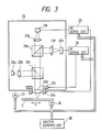
- FIG. 3 of the accompanying drawings is a block diagram showing the construction of an information recording-reproducing apparatus for the optical card as described above.
- a system controller 28 controls motors 26 and 27 and AT and AF servo circuits 24 and 25 to thereby control recording or reproduction of information on the optical card C.
- the motor 26 reciprocally moves the optical card C in the direction of arrow a, whereby a light beam is applied from an optical head 23 along the information tracks of the optical card C.
- the motor 27 is for moving the optical head 23 in a direction perpendicular to the information tracks on the optical card C.
- the optical head 23 has a light source 23a comprising a semiconductor laser, a collimator lens 23b for collimating the light beam from the light source 23a, a beam splitter 23c and an objective lens 23d, and applies a light beam for recording/reproduction onto the recording surface of the optical card C.
- the optical head 23 also has a beam splitter 23e, condensing lenses 23f and 23g, and photoelectric converters 23h and 23i.
- the light beam reflected on the recording surface of the optical card C is received by the photoelectric converters 23h and 23i and converted into electrical signals thereby, and the electrical signals are supplied to the AT servo circuit 24 and the AF servo circuit 25, respectively.
- the AT servo circuit 24 and the AF servo circuit 25 flow driving currents to the tracking actuator 23j and focusing actuator 23k of the optical head 23 to thereby move the objective lens 23d and effective AT and AF control.
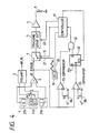
- FIG. 4 of the accompanying drawings shows an example of the prior art relating to the circuits around the above-described AT servo circuit.
- the reference numeral 1 designates a photo-detector for converting a laser light subjected to reflection and modulation on a recording information carrier into an electric current
- the reference numeral 2 denotes a preamplifier for extracting an information signal HF and a focusing error signal FE by the output of the photodetector 1
- the reference numeral 3 designates a tracking error amplifier for extracting a tracking error (AT error) signal from the output of the photodetector 1
- the reference numeral 4 denotes a tracking drive circuit for converting the tracking error signal into a control signal for stably driving a tracking actuator 6
- the reference numeral 5 designates an amplifier
- the reference numeral 7 denotes a change-over switch for changing over the tracking error signal and the output signal 21 of an oscillator 16 by a control signal 19 from a servo controller 15
- the reference numeral 17 designates a comparator
- the reference numeral 32 denotes an AND gate
- the reference numeral 33 designates
- the laser light subjected to reflection and modulation on the information recording carrier includes the recording information and the information regarding a focusing error and a tracking error, and this laser light is photoelectrically converted by the photodetector 1, and a recording information signal and a focusing error signal are extracted by the preamplifier 2.
- the tracking error signal is extracted by the tracking amplifier 3.
- the switch 7 is connected to the tracking servo amplifier 3 side. Accordingly, the tracking error signal is sent to the tracking drive circuit 4 and drives the tracking actuator 6, whereby AT is effected.
- the controller 15 gives an oscillation permission signal 20 to the oscillator 16. At the same time, the controller 15 supplies a control signal 19 for connecting the change-over switch 7 to the output side of the oscillator 16.
- the oscillator 16 outputs a triangular wave to thereby reciprocally move the tracking actuator at a predetermined amplitude and a predetermined speed in a direction across the tracks through the tracking drive circuit 4.
- any change in the AT error signal is input to a comparator 171, and whether the AT error signal has reached a value V1 preset by a voltage varying device 181 is monitored. If the AT error signal exceeds the value V1, the comparator 171 inputs a high level signal to the D flip-flop 33.
- the D flip-flop 33 continues to output a high level signal to the AND gate 32.
- the AT error signal is input to a comparator 172, and whether this signal is below a value V2 preset by a voltage varying device 182 is monitored.
- the comparator 172 outputs a high level signal to the AND gate 32 during a period of time when the AT error signal is below the value V2. That is, the output of the AND gate 32 does not assume a high level until the AT error signal once exceeds the value V1 and then decreases below the value V2.
- the controller 15 sends a change-over signal to the switch 7 to thereby connect the tracking drive circuit 4 to the tracking amplifier 3 and operate the tracking servo.
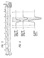
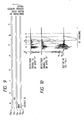
- Figures 5 and 6 of the accompanying drawings illustrate a light beam spot as it relatively crosses the tracks on the recording carrier in the aforedescribed auto tracking-0FF state.
- Figure 5 schematically shows the relative positional relation of information tracks 72 n-1 and 72 n and tracking tracks 73 n-1 - 73 n+1 with the light beam spot, and in the figure, a-h show the manner in which that positional relation changes every moment.
- Figure 6 is a signal waveform graph showing the detection signals of beam spots E and F corresponding to the states a-h and the AT error signal (E-F).
- the beam spots E and F are detected by the reflected lights thereof being received by a photo-electric conversion element 23h shown in Figure 4.
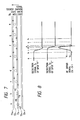
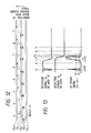
- FIGs 7 and 8 of the accompanying drawings show the circumstances during the process.
- the detection signals of the beams E and F and the AT error signal exhibit the waveforms as shown in Figure 8.
- the AT error signal has become lower than a voltage V2 in the vicinity of 0V after the AT error signal has become greater than a predetermined voltage V1
- the servo loop is closed. Accordingly, from and as shown in Figure 7, the light spot traces the information track 72n.
- the predetermined voltage V1 is determined by the contrast of the information tracks 72 n , 72 n-1 and the tracking tracks 73 n-1 - 73 n+1 .
- the influence of such a defect poses a problem not only when the tracking-ON state is entered from the tracking-0FF state at the start of the operation of the apparatus, but also when track jump is effected.
- the track jump refers to the operation of temporarily switching off the tracking from the state of tracking operation servo and moving the light spot to other track and again restoring the tracking-ON state.
- an optical information processing apparatus comprising: means for scanning tracks formed on an optical recording medium by a light beam; means for moving the applied position of said light beam in a direction across said tracks; means for detecting a tracking error signal indicative of the deviation between the applied position of said light beam and said tracks; tracking servo means for feeding back said tracking error signal to said moving means; switching means for selectively rendering said tracking servo means operative or inoperative; and control means for measuring the time for which said tracking error signal exceeds a predetermined level, and switching said tracking servo means from its inoperative state to its operative state by said switching means after said time exceeds a predetermined time.
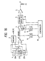
- FIG 11 is a block diagram showing an embodiment of an AT servo circuit used in the optical information processing apparatus of the present invention.
- the apparatus of the present invention can be constructed just like the apparatus of Figure 3, except for this AT servo circuit.
- members identical to those in Figure 4 are given identical reference numerals and need not be described in detail.
- FIG. 11 A block diagram of a tracking control device according to a first embodiment of the present invention is shown in Figure 11. Constituents which are functionally identical to those in the example of the prior art shown in Figure 4 need not be described.
- the reference numeral 7 designates a change-over switch for changing over an AT error signal and the output signal of a D/A converter 9 by a control signal 12 from a servo controller 10
- the reference numeral 171 denotes a comparator for comparing whether the AT error signal output which is the output of a tracking error amplifier 3 is greater than V1
- the reference numeral 172 designates a comparator for comparing whether the AT error signal output is smaller than a predetermined voltage V2
- the reference numeral 29 denotes a presettable voltage varying device capable of being preset by the controller 10 which sets said V1
- the reference numeral 9 designates a D/A converter which outputs an arbitrary voltage 11 to the change-over switch in response to a command from the controller 10
- the reference numeral 13 denotes a control signal output from the controller 10.
- the reference numeral 30 designates a presettable counter.
- the output of the comparator 17 is input to the Enable terminal and Reset terminal of the presettable counter 30.
- the reference numeral 33 denotes a D flip-flop, and Qn terminal is connected to the CK terminal thereof.
- CK one clock time
- x n T
- the time T is chosen so as to be sufficiently longer than a time t1 for which the AT error signal exceeds V1 due to a defect D or the like on the information recording carrier and to be shorter than the time for which the AT error signal exceeds V1 when a light spot crosses tracking tracks.
- Figure 13 is a waveform graph showing variations in the reproduction signals S E and S F of beam spots corresponding to the states a-h in Figure 12 and the AT error signal
- Figure 14 shows the signal waveforms of various portions of the circuit shown in Figure 11.
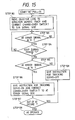
- Figure 15 is a flow chart illustrating such an AT pull-in process.
- the change-over switch 7 is connected to the D/A converter 9 side, and the triangular wave output of the D/A converter 9 flows to a tracking actuator 6, whereby an objective lens begins to move across the tracks (the step 102 of Figure 15).
- the light beam spot F is applied to the defect D and therefore, the AT error signal, as shown in Figure 13, is input to the comparator 171 as a voltage component higher than V1. (At the steps 103 of Figure 15, advance is made to YES.)
- the output of the comparator 171 then assumes a high level and the presettable counter 30 starts to count the clock CK (step 104).
- the beam spot F passes the defect D as shown at b in Figure 12, and the AT error signal becomes smaller than V1.
- the output of the comparator 171 then assumes a low level and the presettable counter 30 is reset.
- t1 «T and therefore, the signal output from the Qn terminal of the counter 30 is at a low level.
- the output of an AND gate 32 also is at a low level, and the controller 10 still continues to move the light spot across the tracks. (At the step 104 of Figure 15, advance is made to NO.)
- the spot F comes to the tracking track and therefore, the AT error signal level increases and exceeds the V1 level. Then the output of the comparator 171 assumes a high level, and the counter 30 starts to count the clock CK.
- the Q D output of the D flip-flop 33 also assumes a high level. (At step 104, advance is made to YES.)
- the output Comp 2 of the comparator 172 assumes a high level.
- step 105 advance is made to YES.
- the output of the AND gate 32 assumes a high level and an interruption signal is output to the terminal IRQ of the controller 10.
- the controller 10 immediately outputs a control signal 12 and connects the change-over switch 7 to the AT error signal side, and effects the change-over to the tracking servo-ON state (the step 106 of Figure 15).
- the controller 10 confirms whether AT failure (out of AT) occurs (step 107), and if AT failure does not occur, the AT operation is continued as shown at e - f in Figure 12 (the step 109 of Figure 15). If AT failure occurs, the tracking servo is rendered into the OFF state (step 108), and return is made to the step 102, where AT pull-in is started again.
- the controller 10 receives this output 34 and outputs a control signal 13 to the tracking drive circuit 4, thereby switching the gain or the like of the circuit 4 in advance.
- FIGS 16 and 17 are block diagrams showing other embodiments of the AT servo circuit used in the optical information processing apparatus of the present invention.
- members identical to those in Figure 11 are given identical reference numerals and need not be described in detail.
- the AT error signal is input to the controller 10 through the A/D converter 8, and the discrimination of the level of the AT error signal and the measurement of the time for which the AT error signal is above a predetermined level are effected by a central processing unit (CPU) in the controller 10 by the use of software.
- CPU central processing unit
- the present embodiment has the effect that although as compared with the first embodiment, the burden of software increases, the discrete parts such as the comparators 17 and the counter 30 become unnecessary and the cost of the apparatus is reduced.
- the reference numeral 8 designates an A/D converter for inputting the AT error signal to the controller 10.
- the reference numeral 14 denotes a sensor for detecting the relative position between the objective lens and the optical head in the direction across the tracks, and this sensor 14 is connected to one contact of the change-over switch 7.
- the reference nuemral 9 designates a D/A converter which connects the controller 10 and the reference of the tracking servo circuit 4.
- the discrimination of the level of the AT error signal and the measurement of the time for which the AT error signal is above a predetermined level are effected by a CPU in the controller 10 by the use of software.
- the D/A output 31 input to the tracking drive circuit 4 is made, for example, into a triangular wave, and the change-over switch 7 is connected to the position sensor 14 side and the objective lens is moved across the tracks in the closed loop by the sensor output of the position sensor 14.
- the present invention permits various applications besides the above-described embodiments.
- the present invention is not restricted to an apparatus using the aforedescribed optical card, but is also applicable to an apparatus using a disk-like or tape-like medium.
- the medium is of the transmission type, design may be made such that the light transmitted through such medium is received by a photodetector to thereby detect the tracking error signal.
- the present invention is also applicable to an apparatus using a magneto-optical recording medium as the medium.
Landscapes
- Optical Recording Or Reproduction (AREA)
- Moving Of The Head For Recording And Reproducing By Optical Means (AREA)
Applications Claiming Priority (2)
| Application Number | Priority Date | Filing Date | Title |
|---|---|---|---|
| JP63255000A JP2656812B2 (ja) | 1988-10-12 | 1988-10-12 | トラッキング制御装置 |
| JP255000/88 | 1988-10-12 |
Publications (2)
| Publication Number | Publication Date |
|---|---|
| EP0364224A1 true EP0364224A1 (fr) | 1990-04-18 |
| EP0364224B1 EP0364224B1 (fr) | 1994-12-21 |
Family
ID=17272809
Family Applications (1)
| Application Number | Title | Priority Date | Filing Date |
|---|---|---|---|
| EP89310371A Expired - Lifetime EP0364224B1 (fr) | 1988-10-12 | 1989-10-11 | Procédé pour fabriquer des informations optiques et appareil ayant un système empêchant une déficience durant le guidage de piste |
Country Status (4)
| Country | Link |
|---|---|
| US (1) | US5077718A (fr) |
| EP (1) | EP0364224B1 (fr) |
| JP (1) | JP2656812B2 (fr) |
| DE (1) | DE68920110T2 (fr) |
Cited By (6)
| Publication number | Priority date | Publication date | Assignee | Title |
|---|---|---|---|---|
| EP0457536A1 (fr) * | 1990-05-15 | 1991-11-21 | Kabushiki Kaisha Toshiba | Milieu d'enregistrement optique et appareil d'enregistrement optique |
| DE4102801A1 (de) * | 1991-01-31 | 1992-08-06 | Thomson Brandt Gmbh | Spurregelkreis |
| US5268887A (en) * | 1990-05-15 | 1993-12-07 | Kabushiki Kaisha Toshiba | Optical recording medium having offset-compensating areas |
| EP0647941A1 (fr) * | 1993-10-08 | 1995-04-12 | Sony Corporation | Appareil pour enregistrer sur un milieu d'enregistrement et procédé pour contrôler l'enregistrement |
| US5619483A (en) * | 1993-01-06 | 1997-04-08 | Sony Corporation | Method of recording on a recording medium employing an automatic termination of recording by monitoring the signal being recorded |
| US5717671A (en) * | 1994-11-30 | 1998-02-10 | Sony Corporation | Apparatus and method for recording constant interval of silence |
Families Citing this family (6)
| Publication number | Priority date | Publication date | Assignee | Title |
|---|---|---|---|---|
| US5327410A (en) * | 1989-09-30 | 1994-07-05 | Deutsche Thomson-Brandt Gmbh | Direction-determination logic as for a signal pickup in recorded signal recovery apparatus |
| GB2248989B (en) * | 1990-10-15 | 1995-05-24 | Applied Magnetics Corp | Focus sensing apparatus and method |
| EP0625077B1 (fr) * | 1992-02-07 | 1997-07-09 | Valleylab, Inc. | Appareil chirurgical a ultrasons |
| KR0132972B1 (ko) * | 1994-11-28 | 1998-04-18 | 배순훈 | 광자기디스크의 서보제어장치 |
| US6606286B1 (en) * | 1998-01-05 | 2003-08-12 | Mitburri Electric Co., Ltd | Tln signal generating apparatus used in optical disc drive and optical disc drive equipped with the apparatus, and optical disc drive equipped with amplitude adjusting apparatus for tracking error signal |
| RU2217842C1 (ru) * | 2003-01-14 | 2003-11-27 | Институт физики полупроводников - Объединенного института физики полупроводников СО РАН | Способ изготовления структуры кремний-на-изоляторе |
Citations (3)
| Publication number | Priority date | Publication date | Assignee | Title |
|---|---|---|---|---|
| EP0244665A2 (fr) * | 1986-04-30 | 1987-11-11 | International Business Machines Corporation | Appareil et méthode de mesure de l'erreur de détection de données |
| EP0258043A2 (fr) * | 1986-08-26 | 1988-03-02 | Canon Kabushiki Kaisha | Support pour l'enregistrement d'information avec un préambule à code de correction d'erreur pour chaque bloc et méthode pour enregistrer l'information sur un tel support |
| EP0261918A2 (fr) * | 1986-09-22 | 1988-03-30 | Canon Kabushiki Kaisha | Procédé et appareil d'enregistrement d'indices de présence ou d'absence d'erreurs dans le porteur aprês contrôle d'erreurs |
Family Cites Families (5)
| Publication number | Priority date | Publication date | Assignee | Title |
|---|---|---|---|---|
| GB2172138A (en) * | 1984-12-29 | 1986-09-10 | Canon Kk | Optical recording-reproducing apparatus |
| US5010534A (en) * | 1984-12-29 | 1991-04-23 | Canon Kabushiki Kaisha | Optical information recording-reproducing apparatus |
| JPH0740363B2 (ja) * | 1985-03-20 | 1995-05-01 | 株式会社日立製作所 | 光学的記録再生装置 |
| US4764860A (en) * | 1985-06-26 | 1988-08-16 | Nippon Gakki Seizo Kabushiki Kaisha | Servo circuit for an information recording and/or reproducing apparatus |
| DE3887601T2 (de) * | 1987-08-31 | 1994-06-09 | Canon Kk | Informationsaufnahme- und/oder -wiedergabegerät mit Mitteln zur Feststellung aller Spurfolgefehler. |
-
1988
- 1988-10-12 JP JP63255000A patent/JP2656812B2/ja not_active Expired - Fee Related
-
1989
- 1989-10-11 EP EP89310371A patent/EP0364224B1/fr not_active Expired - Lifetime
- 1989-10-11 DE DE68920110T patent/DE68920110T2/de not_active Expired - Fee Related
- 1989-10-11 US US07/419,749 patent/US5077718A/en not_active Expired - Lifetime
Patent Citations (3)
| Publication number | Priority date | Publication date | Assignee | Title |
|---|---|---|---|---|
| EP0244665A2 (fr) * | 1986-04-30 | 1987-11-11 | International Business Machines Corporation | Appareil et méthode de mesure de l'erreur de détection de données |
| EP0258043A2 (fr) * | 1986-08-26 | 1988-03-02 | Canon Kabushiki Kaisha | Support pour l'enregistrement d'information avec un préambule à code de correction d'erreur pour chaque bloc et méthode pour enregistrer l'information sur un tel support |
| EP0261918A2 (fr) * | 1986-09-22 | 1988-03-30 | Canon Kabushiki Kaisha | Procédé et appareil d'enregistrement d'indices de présence ou d'absence d'erreurs dans le porteur aprês contrôle d'erreurs |
Cited By (12)
| Publication number | Priority date | Publication date | Assignee | Title |
|---|---|---|---|---|
| EP0457536A1 (fr) * | 1990-05-15 | 1991-11-21 | Kabushiki Kaisha Toshiba | Milieu d'enregistrement optique et appareil d'enregistrement optique |
| US5268887A (en) * | 1990-05-15 | 1993-12-07 | Kabushiki Kaisha Toshiba | Optical recording medium having offset-compensating areas |
| DE4102801A1 (de) * | 1991-01-31 | 1992-08-06 | Thomson Brandt Gmbh | Spurregelkreis |
| US5619483A (en) * | 1993-01-06 | 1997-04-08 | Sony Corporation | Method of recording on a recording medium employing an automatic termination of recording by monitoring the signal being recorded |
| US5625611A (en) * | 1993-01-06 | 1997-04-29 | Sony Corporation | Method of recording on a recording medium employing an automatic updating of management data by monitoring the signal being recorded |
| US5668789A (en) * | 1993-01-06 | 1997-09-16 | Sony Corporation | Recording method of recording medium |
| EP0647941A1 (fr) * | 1993-10-08 | 1995-04-12 | Sony Corporation | Appareil pour enregistrer sur un milieu d'enregistrement et procédé pour contrôler l'enregistrement |
| US5719837A (en) * | 1993-10-08 | 1998-02-17 | Sony Corporation | Apparatus for recording data on a recording medium and for deleting a silent portion of the recorded data |
| US5745462A (en) * | 1993-10-08 | 1998-04-28 | Sony Corporation | Recording apparatus having a recording operation controlled based upon silent portions of inputting data |
| US5886967A (en) * | 1993-10-08 | 1999-03-23 | Sony Corporation | Apparatus for recording data on a recording medium and for deleting a silent portion of the recorded data |
| US6473375B1 (en) | 1993-10-08 | 2002-10-29 | Junichi Aramaki | Method for recording data on a recording medium and for deleting a silent portion of the recorded data |
| US5717671A (en) * | 1994-11-30 | 1998-02-10 | Sony Corporation | Apparatus and method for recording constant interval of silence |
Also Published As
| Publication number | Publication date |
|---|---|
| US5077718A (en) | 1991-12-31 |
| DE68920110T2 (de) | 1995-05-11 |
| DE68920110D1 (de) | 1995-02-02 |
| JPH02103734A (ja) | 1990-04-16 |
| EP0364224B1 (fr) | 1994-12-21 |
| JP2656812B2 (ja) | 1997-09-24 |
Similar Documents
| Publication | Publication Date | Title |
|---|---|---|
| EP0364224B1 (fr) | Procédé pour fabriquer des informations optiques et appareil ayant un système empêchant une déficience durant le guidage de piste | |
| US4982393A (en) | Information recording and/or reproducing apparatus provided with means for detecting abnormality of tracking servo | |
| JPH1097720A (ja) | 情報記録再生装置 | |
| JPH05109085A (ja) | フオーカス制御装置 | |
| CA1314983C (fr) | Appareil optique de traitement d'information pouvant maintenir un dispositif optique dans une situation predeterminee en cas de defaillance de la commande de centrage ou de focalisation | |
| JP2706294B2 (ja) | 光学的情報記録再生装置 | |
| JPH07311948A (ja) | 光学的情報記録再生装置 | |
| US5293366A (en) | Information recording and reproducing apparatus provided with means for adding to a tracking signal offset corresponding to the positional deviation of a recording spot and a reproducing spot | |
| EP0558293B1 (fr) | Méthode d'enregistrement/réproduction optique et appareil pour ceci | |
| JPH05144114A (ja) | 光磁気記録装置 | |
| EP0326343A2 (fr) | Appareil optique d'enregistrement d'information | |
| JP2854131B2 (ja) | 光ビームがデータトラックから離れたことを検知するための方法および光ビームがデータトラックから離れたことを検知するための検知回路 | |
| US5200937A (en) | Apparatus for and method of recording and/or reproducing information by means of two actuators | |
| JP3633635B2 (ja) | 記録担体走査デバイス | |
| KR960007231B1 (ko) | 광 디스크 장치 | |
| US5315569A (en) | Apparatus for recording and/or reproducing information on/from optical card-like information recording medium | |
| JPH0714179A (ja) | 光ディスク装置のフォーカス制御装置 | |
| JP2609721B2 (ja) | 光学式記録情報読取装置 | |
| US5199016A (en) | Method and apparatus for processing data | |
| US5268891A (en) | Optical recording/reproducing apparatus which reduces seek time by timing initiation of tracking control based upon characteristics of record medium vibrations relative to an optical pick-up head | |
| US6711104B2 (en) | Disk reading apparatus | |
| KR100606671B1 (ko) | 광 기록재생기의 액츄에이터 진동 방지 방법 | |
| EP0383562B1 (fr) | Appareil pour l'enregistrement et/ou la reprocuction d'information optique avec dispositif pour interdire le mouvement de la tête optique | |
| KR100628184B1 (ko) | 광 기록재생기의 액츄에이터 제어 장치 | |
| JP2727631B2 (ja) | 速度検出装置 |
Legal Events
| Date | Code | Title | Description |
|---|---|---|---|
| PUAI | Public reference made under article 153(3) epc to a published international application that has entered the european phase |
Free format text: ORIGINAL CODE: 0009012 |
|
| AK | Designated contracting states |
Kind code of ref document: A1 Designated state(s): DE FR GB IT NL |
|
| 17P | Request for examination filed |
Effective date: 19900903 |
|
| 17Q | First examination report despatched |
Effective date: 19930324 |
|
| GRAA | (expected) grant |
Free format text: ORIGINAL CODE: 0009210 |
|
| AK | Designated contracting states |
Kind code of ref document: B1 Designated state(s): DE FR GB IT NL |
|
| PG25 | Lapsed in a contracting state [announced via postgrant information from national office to epo] |
Ref country code: NL Effective date: 19941221 Ref country code: IT Free format text: LAPSE BECAUSE OF FAILURE TO SUBMIT A TRANSLATION OF THE DESCRIPTION OR TO PAY THE FEE WITHIN THE PRE;WARNING: LAPSES OF ITALIAN PATENTS WITH EFFECTIVE DATE BEFORE 2007 MAY HAVE OCCURRED AT ANY TIME BEFORE 2007. THE CORRECT EFFECTIVE DATE MAY BE DIFFERENT FROM THE ONE RECORDED.SCRIBED TIME-LIMIT Effective date: 19941221 |
|
| REF | Corresponds to: |
Ref document number: 68920110 Country of ref document: DE Date of ref document: 19950202 |
|
| ET | Fr: translation filed | ||
| NLV1 | Nl: lapsed or annulled due to failure to fulfill the requirements of art. 29p and 29m of the patents act | ||
| PLBE | No opposition filed within time limit |
Free format text: ORIGINAL CODE: 0009261 |
|
| STAA | Information on the status of an ep patent application or granted ep patent |
Free format text: STATUS: NO OPPOSITION FILED WITHIN TIME LIMIT |
|
| 26N | No opposition filed | ||
| REG | Reference to a national code |
Ref country code: GB Ref legal event code: IF02 |
|
| PGFP | Annual fee paid to national office [announced via postgrant information from national office to epo] |
Ref country code: GB Payment date: 20020927 Year of fee payment: 14 |
|
| PGFP | Annual fee paid to national office [announced via postgrant information from national office to epo] |
Ref country code: DE Payment date: 20021017 Year of fee payment: 14 |
|
| PGFP | Annual fee paid to national office [announced via postgrant information from national office to epo] |
Ref country code: FR Payment date: 20021021 Year of fee payment: 14 |
|
| PG25 | Lapsed in a contracting state [announced via postgrant information from national office to epo] |
Ref country code: GB Free format text: LAPSE BECAUSE OF NON-PAYMENT OF DUE FEES Effective date: 20031011 |
|
| PG25 | Lapsed in a contracting state [announced via postgrant information from national office to epo] |
Ref country code: DE Free format text: LAPSE BECAUSE OF NON-PAYMENT OF DUE FEES Effective date: 20040501 |
|
| GBPC | Gb: european patent ceased through non-payment of renewal fee |
Effective date: 20031011 |
|
| PG25 | Lapsed in a contracting state [announced via postgrant information from national office to epo] |
Ref country code: FR Free format text: LAPSE BECAUSE OF NON-PAYMENT OF DUE FEES Effective date: 20040630 |
|
| REG | Reference to a national code |
Ref country code: FR Ref legal event code: ST |