EP0357080A2 - Phasensynchronisierschaltung in einem Videosignalempfänger und Verfahren zur Herstellung der Phasensynchronisation - Google Patents
Phasensynchronisierschaltung in einem Videosignalempfänger und Verfahren zur Herstellung der Phasensynchronisation Download PDFInfo
- Publication number
- EP0357080A2 EP0357080A2 EP89116190A EP89116190A EP0357080A2 EP 0357080 A2 EP0357080 A2 EP 0357080A2 EP 89116190 A EP89116190 A EP 89116190A EP 89116190 A EP89116190 A EP 89116190A EP 0357080 A2 EP0357080 A2 EP 0357080A2
- Authority
- EP
- European Patent Office
- Prior art keywords
- signal
- output
- frequency
- circuit
- synchronization
- Prior art date
- Legal status (The legal status is an assumption and is not a legal conclusion. Google has not performed a legal analysis and makes no representation as to the accuracy of the status listed.)
- Granted
Links
Images


Classifications
-
- H—ELECTRICITY
- H04—ELECTRIC COMMUNICATION TECHNIQUE
- H04N—PICTORIAL COMMUNICATION, e.g. TELEVISION
- H04N5/00—Details of television systems
- H04N5/04—Synchronising
-
- H—ELECTRICITY
- H04—ELECTRIC COMMUNICATION TECHNIQUE
- H04N—PICTORIAL COMMUNICATION, e.g. TELEVISION
- H04N5/00—Details of television systems
- H04N5/04—Synchronising
- H04N5/12—Devices in which the synchronising signals are only operative if a phase difference occurs between synchronising and synchronised scanning devices, e.g. flywheel synchronising
- H04N5/126—Devices in which the synchronising signals are only operative if a phase difference occurs between synchronising and synchronised scanning devices, e.g. flywheel synchronising whereby the synchronisation signal indirectly commands a frequency generator
-
- H—ELECTRICITY
- H03—ELECTRONIC CIRCUITRY
- H03L—AUTOMATIC CONTROL, STARTING, SYNCHRONISATION OR STABILISATION OF GENERATORS OF ELECTRONIC OSCILLATIONS OR PULSES
- H03L7/00—Automatic control of frequency or phase; Synchronisation
- H03L7/06—Automatic control of frequency or phase; Synchronisation using a reference signal applied to a frequency- or phase-locked loop
- H03L7/08—Details of the phase-locked loop
- H03L7/10—Details of the phase-locked loop for assuring initial synchronisation or for broadening the capture range
- H03L7/113—Details of the phase-locked loop for assuring initial synchronisation or for broadening the capture range using frequency discriminator
Definitions
- the present invention relates generally to a circuit for and a method of providing phase synchronization and, more particularly, to a circuit for and a method of establishing phase synchronization of a horizontal synchronization signal, employed in a video signal receiver such as a TV (a television receiver), an LCD-TV (a liquid crystal display television receiver), or a VTR (a video tape recorder). More specifically, it relates to a circuit for and a method of ensuring establishment of horizontal synchronization even if employed for a video receiver having a matrix type video display such as a liquid crystal display with different numbers of pixels on a line.
- FIG. 1 shows a schematic configuration of a whole television receiver employing the liquid crystal panel as a display device.
- the configuration shown in this figure 1 is, for example, disclosed in Japanese Patent Laying Open Gazette (Kokai) No. 57-41078.
- a liquid crystal panel 101 includes liquid crystal pixels 100 arranged in m rows and n columns.
- the liquid crystal pixels 100 each include a switching transistor 102, a charge holding capacitor 103 and a liquid crystal element 104.
- Gate lines G1-Gm are provided for selecting a particular row of the liquid crystal pixels.
- Source lines S1-Sn are provided for selecting a particular column of the liquid crystal pixels.
- a row driver 105 and a column driver 106 are provided to drive the liquid crystal panel 101.
- the row driver 105 sequentially selects the gate line Gi one by one in response to a control signal from a control signal generator 117.
- the column driver 106 includes a shift register 107, a sample and hold circuit 108 and an amplifier 109.
- the shift register 107 formed of unit shift registers of n stages generates a signal for defining operation timing of the sample and hold circuit 108 in response to the control signal from the control signal generator 117.
- the sample and hold circuit 108 samples and holds video signals (R, G and B) from a video detector 114 in response to clock signals from the shift register 107.
- This sample and hold circuit 108 includes n unit sample and hold circuits provided corresponding to the source lines Sj.
- the amplifier 109 amplifies video information held by the sample and holds circuit 108 to transmit the same onto respective source lines Sj.
- an antenna 110 for receiving video signals a tuner 112, an intermediate frequency amplifier 113, the video detector 114, an audio processing circuit 115, and a loudspeaker 116.
- the tuner 112 selects a frequency band of a desired channel from the received video signals.
- the intermediate frequency amplifier 113 converts the video signals selected through the tuner 112 into a signal of intermediate frequency and amplifies the same to be transmitted to the video detector 114.
- the video detector 114 detects a video signal from a composite video signal converted into this intermediate frequency, and also separates an audio signal from the video signal to supply the same to the audio processing circuit 115.
- the audio processing circuit 115 detects and reproduces this audio signal to supply the same to the loudspeaker 116.
- the video signal from the video detector 114 is applied to the sample and hold circuit 108.
- the control signal generator 117 separates a synchronization signal (a horizontal and vertical signal) from the video signal received from the video detector 114 and derives a signal required for driving the rows and columns of the liquid crystal panel 101. An operation will then be described briefly.
- a video signal shown in Fig. 2 (A) is applied from the video detector 114.
- the video signal has a vertical synchronization signal period T1, a vertical fly-back period T2 and a video signal period T3.
- the video signal period T3 includes horizontal synchronization signals.
- the control signal generator 117 generates a signal (Fig. 2 (B)) indicating initiation of one field in response to the first horizontal synchronization signal after the vertical period T2 is completed. Accordingly, the initiation of the one field is detected.
- the control signal generator 117 subsequently generates a clock signal (Fig. 2 (C)) of a period 1H (H: one horizontal scanning period).
- the row driver 105 In response to this clock signal (a scanning clock signal), the row driver 105 generates signals (Fig. 2 (D) to (F)) for sequentially raising the gate line Gj in potential. Accordingly, only a single gate line Gi is selected during one horizontal scanning period.
- the switching transistors 102 connected to this particular row are turned on during a horizontal fly-back period, so that the pixel information transmitted onto the source lines S1-Sn is transmitted onto the respective liquid crystal elements 104.
- an operation waveform diagram of the column driver 106 is as shown in Fig. 3.
- the column driver 106 repeats the same operation for each 1H period.
- the video signal in the 1H period includes a horizontal synchronization signal period and horizontal fly-back period T4, and a period T5 during which a video information is transmitted.
- clock signals sequentially shifted by T in the phase are outputted from an output of each stage of the shift register 107.
- the clock signals (Figs. 3 (D) through 3 (F)) from the shift register 107 are applied to the sample and hold circuit 108.
- the sample and hold circuit 108 samples the video signal derived from the video detector 114 and holds the same during the 1H period. Accordingly, information corresponding to a row of pixels is held in the sample and hold circuit 108. This pixel information is in parallel transmitted via the amplifier 109 onto the source lines S1-Sn.
- each of the clock signals generated by the control signal generator 117 may be selectively generated corresponding to the number of the pixels.
- a general-purpose control signal generator it is necessary to employ a circuit configured in consideration of changes in the number, n, of the pixels in a row.
- Fig. 4 shows an example of a conventional circuit configuration for generating horizontal synchronizing clock signals which can be employed for various kinds of the liquid crystal panels.
- One of ICs (integrated circuits) for horizontal phase synchronization having such configuration as shown in Fig. 4 is ⁇ pD6109G, a product of by NEC (Nihon Electronics Corp).
- a conventional horizontal phase synchronizing circuit includes a synchronization separating circuit 14 at its input stage.
- the synchronization separating circuit 14 receives a video signal via a coupling capacitor C5 to extract a synchronization signal (horizontal and vertical).
- the horizontal phase synchronizing circuit further includes a first PLL (Phase Locked Loop) loop and a second PLL loop.
- PLL Phase Locked Loop
- the first PLL loop includes a first phase comparator 16, a first lowpass filter 18, an adjuster 20, a first voltage control type oscillator 22, and a 1/2 frequency divider 24.
- the phase comparator 16 compares in phase a horizontal synchronization signal from the synchronization separating circuit 14 with a signal of a frequency 15.73KHz from the 1/2 frequency divider 24.
- the phase comparator 16 is of pulse width detecting type for only comparing the phases of applied signals and has a characteristic immune to noise.
- the first lowpass filter 18 includes capacitors C1 and C2 and resistors R1 and R2.
- the resistor R2 is provided between a terminal PCO and a node N1.
- the resistor R1 and the capacitor C2 are provided in series between the node N1 and a ground potential.
- the capacitor C1 is provided in parallel to a series body of the resistor R1 and the capacitor C2.
- the lowpass filter 18 removes noises included in an output signal of the phase comparator 16 and generates a direct current control voltage.
- the adjuster 20 includes resistors R3 and R4 and a variable resistor VR1.
- the resistor R3 is provided between an output of the lowpass filter 18 and a node N2.
- the variable resistor VR1 and the resistor R4 are provided in series between the node N2 and the ground potential.
- This adjuster 20 has a function of controlling an oscillation phase of the voltage control type oscillator 22. That is, adjustment of a resistance value of the variable resistor VR1 adjusts advancing or delaying in phase of an output signal of the voltage control type oscillator 22.
- the voltage control type oscillator 22 oscillates with a frequency twice as large as the horizontal scanning frequency (15.73KHz).
- the 1/2 frequency divider 24 frequency-divides, by a factor of 2, an output of the first voltage control type oscillator 22 to output a quasi-horizontal synchronization signal f H to the phase comparator 16.
- the phase comparator 16 which is of the pulse width detecting type as described above, has an output characteristic having a plurality of slopes (S curves) as shown in Fig. 5.
- the abscissa designates an input signal frequency
- the ordinate designates an output voltage
- f0 represents a reference signal.
- the phase comparator 16 provides an output voltage with the same output characteristics also in the case that the input signal frequency to the phase comparator becomes twice or three times the frequency of the reference signal (the horizontal synchronization signal). Therefore, the first PLL loop has lock ranges corresponding to the respective S curves, and thus the first voltage control type oscillator 22 shown in Fig. 4 sometimes oscillates with the frequency twice or three times that in a normal time to become stable.
- the oscillation frequency range of the first voltage control type oscillator 22 is set to the range of the frequency from f1 to f0 shown in Fig. 5.
- the second PLL loop of the horizontal phase synchronizing circuit includes a phase/frequency comparator 26, a second lowpass filter 28, a second voltage control type oscillator 30 and a programmable counter 32.
- the phase/frequency comparator 26 compares in phase and frequency a horizontal scanning signal from the 1/2 frequency divider 24 with an output of the programmable counter 32.
- the second lowpass filter 28 includes a resistor R5 and a capacitor C3. The resistor R5 and capacitor C3 are connected in series between a terminal PFCO and the ground potential.
- the second lowpass filter 28 removes undesirable high frequency components such as noise components included in the phase/frequency comparator 26, and provides a direct current voltage signal only indicating a result of this comparison so as to apply the same to a voltage control terminal VCOH of the second voltage control type oscillator 30.
- the second voltage control type oscillator 30 having a large oscillation frequency range oscillates normally with the frequency n times the horizontal scanning frequency.
- the programmable counter 32 frequency-divides, by a factor of n, an output of the second voltage control type oscillator 30 to derive a signal with the horizontal frequency and transmit the same to the phase/frequency comparator 26, and also applies this n ⁇ f H (f H is a quasi horizontal scanning frequency signal) to a programmable logic array 33.
- the programmable logic array 33 provides a horizontal driving clock signal HCLOCK for driving the column driver 106 shown in Fig. 1.
- the n corresponds to the number of the pixels in a row. Therefore, the value of the n varies depending on the varied number of the pixels of the liquid crystal panel.
- the oscillation frequency band of the second voltage control type oscillator 30 is designed to have a large width so as to correspond to the various kinds of the liquid crystal panels.
- the phase/frequency comparator 26 compares not only the phases but also the frequencies.
- This comparator 26 has an output characteristic having only a single slope (an S curve) as shown in Fig. 6.
- the abscissa indicates an input signal frequency
- the ordinate indicates an output voltage. Since the phase/frequency comparator 26 also functions with a frequency error detector, as apparently seen from Fig. 6, the second voltage control type oscillator 30 does not oscillate with the frequency twice or three times the frequency in the normal time (nf H ). That is, the second PLL loop has only one lock range so that it can oscillate at a stable state with a desired oscillation frequency.
- the conventional horizontal phase synchronizing circuit shown in Fig. 4 as described above requires two comparators 20 and 30.
- an output of the synchronization separating circuit 14 is directly applied to the phase/frequency comparator 26.
- the following problems occur in such configuration as above. That is, in receiving a strong electric field signal as shown in Fig. 7 (a), the output of the synchronization separating circuit 14 does not include noises, thereby obtaining a stable oscillating signal synchronized in phase with a horizontal synchronization signal.
- a weak electric field signal as shown in Fig.
- the output of the synchronization separating circuit 14 includes noises, so that an output of the phase/frequency comparator 26 is affected adversely by the noises, and thus the oscillation frequency of the voltage control type oscillator is fixed to its upper limit value or lower limit value. This causes a problem that the oscillating signal synchronized in phase with a desired horizontal synchronization signal cannot be obtained.
- the phase comparator 16 Even in a case that the horizontal synchronization signal including noises in receiving the weak electric field signal is inputted to the phase comparator 16 immune to noises, the phase comparator 16 outputs noise components due to a random noise. However, since the lowpass filter 18 cancels the noise components, it resultantly outputs only phase comparison components with regularity of the normal horizontal synchronization signal and the quasi horizontal synchronization signal. Thus, the voltage control type oscillator 22 oscillates with a desired oscillation frequency (31.5KHz) in the first PLL loop, resulting in a quasi horizontal synchronization signal having the same frequency and phase as the horizontal synchronization signal.
- a desired oscillation frequency (31.5KHz)
- Japanese Patent Laying Open Gazette No. 57-41078 discloses a method of generating a horizontal driving pulse in synchronization in phase with the horizontal synchronization signal in a matrix type television.
- Japanese Patent Laying Open Gazette No. 57-8161 similarly discloses a method of providing a signal synchronized in phase with the horizontal synchronization signal by employing a PLL loop, as a horizontal driving pulse signal of a liquid crystal matrix display panel.
- the phase synchronizing circuit comprises a circuit for separating and extracting at least a horizontal synchronization signal from an applied video signal, a first PLL loop relatively immune to noise for providing a signal synchronized in phase with the separated/extracted horizontal synchronization signal, and a second PLL or AFC loop for receiving the separated/extracted horizontal synchronization signal via a bandpass filter to provide a signal at least frequency-locked to an output of this bandpass filter.
- the first PLL loop shares with the second PLL or AFC loop in a voltage control type oscillator and a frequency divider.
- the phase synchronizing circuit further comprises detecting circuitry for deciding whether or not the separated/extracted horizontal synchronization signal is in synchronization with an output of the frequency divider, and circuitry for activating either one of the first PLL loop or the second PLL or AFC loop in response to an output of the synchronization deciding circuitry.
- the first PLL loop comprises a first comparator comparatively immune to noise, having an output characteristic with a plurality of S curves.
- the first comparator compares in phase the separated/extracted horizontal synchronization signal with the frequency divider output.
- the second PLL or AFC loop comprises a second comparator having an output characteristic with a single S curve.
- the second comparator compares the bandpassed horizontal synchronization signal with the frequency divider output at least in frequency.
- the first comparator is formed of a pulse width type detector relatively immune to noises.
- the second comparator is formed of an edge trigger type detector or a frequency edge trigger type phase comparator.
- the second comparator is also formed of a frequency comparator which compares frequencies of applied signals.
- the phase synchronizing circuit further comprises circuitry for generating a quasi horizontal synchronization signal with a frequency same as that of the horizontal synchronization signal, and circuitry responsive to an output of the synchronization detector and a signal with its level inverted at a predetermined period for selecting one of an output of the bandpass filter and the quasi horizontal synchronization signal to supply the selected one to the second comparator.
- a method of phase synchronization according to the present invention comprises the step of activating the first PLL loop when the synchronization detector is detecting a synchronizing state, and activating the second PLL loop when the synchronization detector is detecting a non-synchronizing state.
- the second PLL or AFC loop having a single lock range is activated, and the voltage control type oscillator is controlled by the noise-removed horizontal synchronization signal having a time delay caused by the bandpass filter. Accordingly, a signal which is frequency-locked to a received horizontal synchronization signal is first outputted from the frequency divider.
- the first PLL loop is activated by the output of the synchronization detector. Consequently, a signal is outputted from the frequency divider, which is locked in phase and frequency to the received horizontal synchronization signal due to the function of the first PLL loop.
- the bandpass filter is not provided in the first PLL loop, a time delay does not occur corresponding to the horizontal synchronization signal, resulting in a reliably phase-locked signal.
- an oscillation frequency and phase of the voltage control type oscillator can be fixed by controlling the voltage control type oscillator by employing the quasi horizontal synchronization signal, so that a fluctuation does not occur in a reproduced picture in this state.
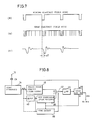
- Fig. 8 shows a principle configuration of a horizontal phase synchronizing circuit according to the present invention.
- the horizontal phase synchronizing circuit comprises a synchronization separating circuit 14, a phase comparator 16, a phase/frequency comparator 26, a bandpass filter 40, a switching circuit 42, a lowpass filter 44, a voltage control type oscillator 46 and a synchronization detector 48.
- the synchronization separating circuit 14 receives via a coupling capacitor C5 a video signal applied via an input terminal 12 and extracts a synchronization signal (a horizontal synchronization signal) to apply the same to the phase comparator 16.
- the phase comparator 16 which is a pulse width detecting type phase comparator having an output characteristic as shown in Fig. 5, compares the phase of the horizontal synchronization signal from the synchronization separating circuit 14 with that of an output of the voltage control type oscillator 46 to output a signal corresponding to a difference in these phases.
- a received horizontal synchronization signal with its noise components removed by the bandpass filter 40 is applied to the phase/frequency comparator 26 and the synchronization detector 48.
- the phase/frequency comparator 26 having an output characteristic shown in Fig. 6 compares the phase and frequency of the horizontal synchronization signal from the bandpass filer 40 with those of the output of the voltage control type oscillator 46.
- the synchronization detector 48 compares the received horizontal synchronization signal with the voltage control type oscillator 46 via the bandpass filter 40 and generates a signal indicating whether or not the output of the voltage control type oscillator 46 is in synchronization with the received horizontal synchronization signal.
- This synchronization detector 48 is a circuit for detecting the fact that the output signal of the voltage control type oscillator 46 attains a normal horizontal synchronization frequency (15.73KHz), and also compares the phases of the output of the voltage control type oscillator and of the received horizontal synchronization signal. That is, the synchronization detector 48 detects the presence or absence of the received horizontal synchronization signal from the bandpass filter 40 when the output of the voltage control type oscillator 46 rises, and decides that synchronization is established when the received horizontal synchronization signal exists during a predetermined period.
- the switching circuit 42 responds to an output of the synchronization detector 48, by connecting a contact thereof to the contact e or f.
- the switching circuit 42 has its contact connected to the f in the case of that the synchronization detector 48 is detecting a non-synchronizing state, but to the e in the case that the detector 48 is detecting a synchronizing state.
- the lowpass filter 44 applies a direct current control voltage obtained by removing the high frequency components included in an output of the switching circuit 42, to a voltage control terminal of the voltage control type oscillator 46.
- the voltage control type oscillator 46 which is not illustrated in detail, includes a 1/n frequency divider to output a horizontal frequency signal f H with the frequency 15.73KHz and a frequency n ⁇ f H for generating a horizontal driving pulse corresponding to the number of pixels.
- the signal of the frequency n ⁇ f H is transmitted to a programmable logic array (PLA), and thus the horizontal pulse is produced therein.
- PLA programmable logic array
- a first PLL loop is constituted by the phase comparator 16, the switching circuit 42, the lowpass filter 44 and the voltage control type oscillator 46.
- a second PLL loop is constituted by the phase/frequency comparator 26, the switching circuit 42, the lowpass filter 44 and the voltage control type oscillator 46.
- An output of the bandpass filter 40 is applied to the synchronization detector 48 in the configuration shown in Fig. 8.
- the synchronization detector 48 comprises itself a function of removing noise components, it may be configured such that a received horizontal synchronization signal separated by the synchronization separating circuit 14 is directly applied to the synchronization detector 48 as shown by the broken line in Fig. 8.
- the synchronization detector 48 performs a phase comparing operation as described above, it can also be configured that a part of the circuit configuration thereof is shared with the phase/frequency comparator 26. An operation will then be described.
- the non-synchronizing state is provided at an operation starting time.
- the synchronization detector 48 outputs a signal of the L level indicating the non-synchronizing state to apply the same to the switching circuit 42.
- the switching circuit 42 connects its contact to the f in response to this switching control signal of the L level. Accordingly, the second PLL loop first starts operating.
- a received horizontal synchronization signal is applied to the phase/frequency comparator 26 via the bandpass filter 40.
- the bandpass filter 40 removes the noise components to extract the horizontal synchronization signal components. Therefore, although the deviation ⁇ T (see Fig. 7) occurs in this case, an oscillation frequency of the voltage control type oscillator 46 is captured in the frequency of the received horizontal synchronization signal.
- the phase/frequency comparator 26 performs not only a frequency comparison but also a phase comparison, the output of the voltage control type oscillator 46 has its output signal phase also captured in the received horizontal synchronization signal to some extent.
- the synchronization detector 48 decides that the synchronization is established, so that it outputs a signal of the H level. Accordingly, the switching circuit 42 has its contact switched to the contact e, so that the first PLL loop (including the phase comparator 16, the lowpass filter 44 and the voltage control type oscillator 46) starts operating.
- the phase comparator 16 in the first PLL loop compares the phase of a received horizontal synchronization signal from the synchronization separating circuit 14 with that of a horizontal frequency signal f H from the voltage control type oscillator 46 and outputs a signal corresponding to the difference between these phases. Accordingly, the phase control is carried out by the first PLL loop, so that a signal is outputted from the voltage control type oscillator 46, which is synchronized in phase and frequency with the received horizontal synchronization signal.
- the output of the voltage control type oscillator 46 is so controlled by operating the second PLL loop that the first PLL loop can capture at least the oscillation frequency of the voltage control type oscillator 46 into a normal oscillation frequency (15.73KHz) thereof, in the present invention. Therefore, the voltage control type oscillator 46 does not erroneously oscillate at the stable state with the frequency twice or three times the normal frequency (15.73KHz), thereby obtaining a horizontal driving pulse reliably synchronized in phase with the received horizontal synchronization signal.
- the received horizontal synchronization signal from the synchronization separating circuit 14 is directly applied to the phase comparator 16 without passing through the bandpass filter 40, thereby preventing the occurrence of the deviation in time ⁇ T (see Fig. 7) caused by the bandpass filter.
- phase/frequency comparator is employed in the second PLL loop; however, it can be replaced by a comparator with the output characteristic shown in Fig. 6, such as an edge trigger type phase comparator, or a frequency comparator.
- the voltage control type oscillator 46 has its output signal phase changed.
- this is such a very small change that the synchronization detector 48 keeps outputting the signal of the H level indicating the synchronization detecting state.
- a comparator may be employed as the phase/frequency comparator 26, which serves as the frequency comparator in the PLL unlock and as the phase comparator in the PLL lock.
- the comparator having such configuration is, for example, MC4044, PC2 of CD74HC4046A, PC2 of CD4046A etc. manufactured by Motorola, Inc.
- Fig. 9 schematically shows a detailed configuration of the horizontal phase synchronizing circuit according to one embodiment of the present invention.
- those corresponding to the circuits shown in the Fig. 8 are denoted with like reference numerals.
- the synchronization separating circuit 14 corresponds to a synchronization separating circuit 201, an H gate 203 and an H filter 202.
- the bandpass filter 40 in Fig. 8 corresponds to an H window 40′.
- the voltage control type oscillator 46 in Fig. 8 corresponds to a voltage control type oscillator 46′ and a programmable counter 204.
- Phase comparator 16 is pulse width type phase detector, and a comparator 26 is an edge trigger type phase detector.
- the H filter 202 removes noise components included in a synchronization signal (a horizontal and vertical synchronization signal) CSYNC separated from the synchronization separating circuit 201 to apply the signal to the H window 40′.
- the H gate 203 passes therethrough a received horizontal synchronization signal from the synchronization separating circuit 201 in response to signals from an H gate pulse generator 206 and a synchronization detector 48.
- the H gate 203 passes therethrough all the outputs of the synchronization separating circuit 201 in the case that the synchronization detector 48 is detecting the non-synchronizing state, while it passes therethrough the output of the synchronization separating circuit 201 only during a period that a pulse signal is applied from the H gate pulse generator 206 in the case that the synchronization detector 48 is detecting the synchronizing state.
- the H gate pulse generator 206 generates a signal with a larger signal width than and the same frequency as a normal horizontal synchronization signal HSYNC in response to an output signal from the programmable counter 204.
- the H gate pulse generator 206 is, for example, formed by employing a PLA (Programmable Logic Array).
- the programmable counter 204 which is a circuit for providing a frequency dividing ratio of an output of the voltage control type oscillator 40′, sets the frequency dividing ratio n corresponding to the number of pixels of the liquid crystal display panel employing this horizontally phase synchronizing circuit.
- the output from the programmable counter 204 is supplied to an H ⁇ PLA205 to be subject to a predetermined logic processing, thereby generating a horizontal driving pulse HCLOCK synchronized in phase with the received horizontal synchronization signal.
- the H window 40′ serving as a bandpass filter having its center frequency as a horizontal synchronization signal frequency, is formed by employing a digital filter for integration of a circuit configuration.
- the operation of the circuit shown in Fig. 9 is similar to that shown in Fig. 8, however, it will briefly be described as follows.
- the non-synchronizing state is provided at the operation starting time. Therefore, a signal H ⁇ KILLER indicating the synchronizing state from the synchronization detector 48 is in the L level.
- the H gate 203 passes therethrough all the synchronization signals applied from the synchronization separating circuit 201.
- a synchronization signal from the synchronization separating circuit 201 has then its noise components removed by the H filter 202 and the H window 40′, and then a frequency component corresponding to the horizontal synchronization signal is applied to the edge trigger type phase/frequency comparator 26.
- a switching circuit 42 has its contact connected to the contact f. Therefore, the second PLL loop operates and thus the oscillation frequency of the voltage control type oscillator 46′ is captured in the frequency n ⁇ f H .
- the programmable counter 204 frequency-divides, by a factor of n, an oscillating signal from the voltage control type oscillator 46′ to output as a quasi horizontal synchronization signal f H .
- the output signal H KILLER thereof rises to the H level.
- the switching circuit 42 has its contact switched to the contact e, and also the H gate 203 passes therethrough a applied signal only during the period of an H gate signal H GATE from the H gate pulse generator 206. Due to this function of the gate 203, the received horizontal synchronization signal has its noise components removed to be transmitted to the phase comparator 16. Accordingly, the first PLL loop functions to capture the oscillating signal of the voltage control type oscillator 46′ into the normal oscillation frequency and phase and thus to keep stable oscillation.
- the H filter 202 removes undesirable noise components from the output of the synchronization separating circuit 201; however, the H filter 202 need not particularly be provided if the H window 40′, the synchronization detector 48 and so on at the succeeding stage are immune to the noise components.
- the lowpass filter 44 is provided between the switching circuit 42 and the voltage control type oscillator 46′ in the configuration of Fig. 9. However, in place of this configuration, two lowpass filters may be provided at the succeeding stages of the phase comparator 16 and the phase/frequency comparator 26, respectively, so as to have their outputs selected in the switching circuit 42 to be supplied to the voltage control type oscillator 46′.
- Fig. 10 shows an example of the detailed configuration of the H window 40′.
- the H window 40′ comprises five stages of cascade-connected T type flipflops (T-FF) 329, 330, 331, 332 and 333 for counting clock signals CLK externally applied (e.g., the frequency of 3.58MHz).
- the T-FFs 329-332 have their respective Q outputs transmitted to the respective T inputs of the T-FFs 330-333 at their succeeding stages. Therefore, the T-FF332 has its Q output provide a signal that the clock signal CLK is frequency-divided by 16 (in the case that the T-FFs 329-333 are not reset in response to the horizontal synchronization signal CSYNC).
- the T-FFs 329-332 have their Q outputs transmitted to OR gates OG1-OG3, respectively.
- the OR gate OG1 receives the respective Q outputs of the T-FFs 329-332.
- the OR gate OG 2 receives the outputs of the T-FFs 329, 330 and 332.
- the OR gate OG3 receives the Q output of T-FF329 and a signal of the Q output of the T-FF332 transmitted via an inverter IV1.
- OR gate OG4 set/reset flipflops 334, 335 and 336, AND gates AG1 and AG2 and NAND gate NG1 are provided to supply reset timings of the counters (T-FFS 329-333) and the horizontal synchronization signal HSYNC through the comparator 26 of the succeeding stage.
- the OR gate OG4 receives a signal of the output of the OR gate OG1 transmitted via an inverter V2, and a synchronization signal CSYNC (a horizontal and vertical synchronization signal) from the H filter 202.
- the set/reset flipflops 334-336 are each formed of a D type flipflop (D-FF).
- the set/reset flipflop 334 (hereinafter simply referred to as a SR - FF) has its D input and C input connected to the supply potential Vcc, its set input S receive an output of the OR gate OG2, and its reset input R receive a Q output of the SR - FF335.
- the SR - FF335 has its D input and C input connected to the supply potential Vcc, its set input S connected to a Q output of the SR - FF334, and its reset input R connected to an output of the NAND gate NG1.
- the SR FF336 has its D input and C input connected to the supply potential Vcc, each set input S connected to the output of the OR gate OG2, and its reset input R connected to the output of the OR gate OG3.
- a Q output of the SR - FF336 is applied to the AND gate AG2.
- the AND gate AG1 receives the Q output of the SR FF334 and the Q output of the SR - FF335.
- the NAND gate NG1 receives outputs of the AND gate AG1 and OR gate OG4, respectively.
- the AND gate AG2 receives the Q output of the SR - FF336 and the synchronization signal CSYNC from the H filter 202.
- the output of the AND gate AG2 is applied to the comparator 26 and the synchronization detector 48.
- the T-FFs 329-333 invert the levels of the respective Q outputs everytime the clock signals CLK are applied to their T inputs, and also output signals of "1" from their Q outputs when reset signals are applied to their reset terminals R . Therefore, the T-FFs329 - 333 constitute a counter for counting 32 clock signals CLK as far as the reset signals are not applied thereto.
- the OR gates output signals of the H level when at least one of input signals attains the H level. That is, the OR gates OG1 - OG3 each outputs a signal of the L level when all the supplied input signals are in the L level. Therefore, when the counter (T-FFs329 - 333) counts eleven clock signals CLK, all the inputs of the OR gate OG2 attain the L level, and its output (a node Q3) attains L level. Accordingly, the SR - FF334 is set, so that the Q output attains the H level.
- the counter (T-FFs329 - 333) performs the counting operation independent of receipt of a synchronization signal CSYNC from the H filter 202. Consequently, it can prevent the noise included in the synchronization signal CSYNC and a video-in-sync phenomenon that the video signal is deviated into the period of the synchronization signal.
- the SR - FF336 is reset responsive to the output of the OR gate OG2 (the node Q3) in counting 11 clock signals, the output of a node Q1 attains the H level.
- the SR - FF336 is reset by the output of OR gate OG3 (the node Q4) and thus the potential on the node Q1 falls to the L level. Therefore, the AND gate AG2 is supplied from the SR - FF336 with a gate signal which corresponds to the period when the horizontal synchronization signal will be applied in a normal time.
- the synchronization signal CSYNC (correctly HSYNC) from the H filer 202 is outputted to be transmitted to the comparator 26 and the synchronization detector 48.
- This capture of the horizontal synchronization signal ranges from 11 to 15 of the count values of the clock signals CLK. It becomes possible unlike an analogue filter by employing the H window circuit of this configuration to implement a bandpass filter for passing only a desired frequency band (a signal band having the horizontal synchronization signal as its center frequency) in a highly integrated circuit configuration.
- phase comparator 16 is formed of the pulse width type phase detector
- phase/frequency comparator 26 is formed of the edge trigger type phase detector.
- the phase comparator 16 includes AND gates AN10 and AN11, and inverters IV10 and IV11.
- the AND gate AN10 receives a synchronization signal CYSNC from the H gate 203 and a quasi horizontal synchronization signal f H from the programmable counter 204.
- the AND gate AN11 receives the quasi horizontal synchronization signal f H via the inverter IV10 and also the synchronization signal CSYNC from the H gate 203.
- the inverter IV11 inverts an output of the AND gate AN10 to transmit the same.
- the comparator 26 includes D flip-flops 340 and 341, NOR gates NR1, NR2 and NR3, and an inverter IV12.
- the D type flip-flop (hereinafter simply referred to as the D-FF) 340 has its clock input C receive the quasi horizontal synchronization signal f H and its D input connected to the ground potential.
- the D-FF341 has its clock input C receive a synchronization signal CSYNC from the H window 40′ and its D input connected to the supply potential Vcc.
- the D-FF340 has its Q output supply a signal of the L level each time the signal f H is applied to its clock input terminal C.
- the D-FF341 has its Q output provide a signal of the L level each time the synchronization signal CSYNC is applied to its clock input terminal C. Therefore, the D-FFs340 and 341 are triggered at the rising edges of the signals f H and CSYNC, respectively, to change their output states.
- the NOR gate NR1 receives the Q output of the D-FF340 and the Q output of the D-FF341.
- the output of the NOR gate NR1 is applied via the inverter IV12 to a set input S of the D-FF340 and a reset input R of the D-FF341.
- the NOR gate NR2 receives an output of the NR gate NR1 and a Q output of the D-FF340.
- the NOR gate NR3 receives the Q output of the D-FF341 and the output of the NOR gate NR1. An operation will then be described.
- the quasi horizontal synchronization signal f H is synchronized in phase with the received horizontal synchronization signal HSYNC when a pulse width of a signal appearing on the node A is equal to that of a signal appearing on the node B.
- the phase comparator 16 of the pulse width type detects a difference in phase between the received synchronization signal CSYNC and the quasi horizontal synchronization signal f H in accordance with a difference in pulse width between the signals on the nodes A and B.
- the PLL loop including this phase detecting comparator 16 oscillates stably. Furthermore, as can be seen in this configuration, this comparator 16 is not affected by noises and be able to perform phase comparison, however, it provides the same output characteristic to a sideband (a high harmonic 2f H , 3f H ...) of the quasi horizontal synchronization signal f H .
- the D-FF340 outputs a signal of the L level everytime the quasi horizontal synchronization signal f H is applied thereto, while the D-FF341 outputs a signal of the L level everytime the synchronization signal CSYNC is applied thereto.
- the D-FFs340 and 341 both transmit their output signals to the NOR gate NR1.
- the NOR gate NR1 outputs a signal of the H level only when its two inputs are both in the L level. In such a timing relation as shown in Fig.
- the inputs of the NOR gate NR1 both attained the L level when the Q output of the D-FF340 attain the L level, so that the D-FF340 is set via the inverter IV12, but the D-FF341 is reset. Therefore the potential on a node E instantly falls to the L level each time this quasi horizontal synchronization signal f H is applied thereto, while the potential on a node F is in the L level during the period of the phase difference between the synchronization signal CSYNC and the quasi horizontal synchronization signal f H . As a result, the potential on a node D is fixed to the L level, and the potential on a node C attains the same signal waveform as that of the node A.
- Fig. 13B shows an example of the case that the frequency of the quasi horizontal synchronization signal f H is half that of the received horizontal synchronization signal CSYNC.
- a signal shifted by one period of the received synchronization signal appears in the same phase as that of the horizontal synchronization signal f H on each of the nodes A and B.
- a signal of the L level is outputted to the node C, and an inverted signal of the quasi horizontal synchronization signal f H appears on the node D.
- the outputs of the phase comparator 16 and the phase /frequency comparator 26 are switched over by employing three-state buffers TB1-TB4 constituting the switching circuit 42.
- Each of the three-state buffers TB1-TB4 is rendered conductive when a signal of the L level applied to their control terminals; otherwise their outputs become a high impedance state.
- the buffer TB1 receives the output of the NOR gate NR2 via an inverter IV50, and the buffer TB2 receives the output of the NOR gate NR3.
- the buffer TB3 receives the output of the AND gate AN10 via an inverter IV11, and the buffer TB4 receives the output of the AND gate AN11.
- the three-state buffers TB1 and TB2 have their control terminals supplied with a synchronization detecting signal H ⁇ KILLER from the synchronization detector 48, while the three-state buffers TB3 and TB4 have their control terminals supplied with the synchronization detecting signal H ⁇ KILLER via an inverter IV20. Therefore, the three-state buffers TB1 and TB2 are rendered conductive so as to select the output of the phase/frequency comparator 26 in the non-synchronizing state, while the three-state buffers TB3 and TB4 are rendered conductive to select the output of the phase comparator 16 in the synchronizing state.
- the lowpass filter 44 includes a p channel MOS transistor PT1 and an n channel MOS transistor NT1 at its input stage.
- the p channel MOS transistor PT1 and the n channel MOS transistor NT1 are complementarily connected to each other between a supply potential Vcc and the ground potential.
- the p channel MOS transistor PT1 has its gate supplied with an output of the switching circuit 42, i.e, the potential on a node U.
- the n channel MOS transistor NT1 has its gate supplied with the potential on an output node V of the switching circuit.
- the potential on a connecting point of the p channel MOS transistor PT1 and n channel MOS transistor NT1 is transmitted via resistors R11 and R12 to an inverter IV30.
- An analog switch AS1 is provided in parallel to the resistor R12.
- the analog switch AS1 has its control terminal supplied with synchronization detecting signal H ⁇ KILLER from the synchronization detector 48 via an inverter IV31.
- a capacitor C10 and a resistor R13 are connected in series between a node I (the connecting point of the resistor R12 and the inverter IV30) and a ground potential.
- a series body of the analog switch AS2 and a resistor R14 is provided in parallel to the resistor 13.
- a capacitor C11 is provided between the node I and the ground potential.
- the analog switch AS2 has its control terminal received the synchronization detecting signal H ⁇ KILLER from the synchronization detector 48.
- N channel MOS transistor NT2 resistors R20 and R21 are provided to invert an output of the inverter IV30 and transmit the same.
- the output of the inverter IV30 is transmitted to the gate of the n channel MOS transistor NT2.
- a direct control voltage signal is transmitted from the connecting point of the resistors R20 and R21 to a voltage control terminal of the voltage controlled oscillator 46′.
- the analog switches AS1 and AS2 are rendered conductive when a signal of the H level is applied to their control terminals.
- the lowpass filter 44 has a function of converting the output of the comparator 26 or 16 into a direct current potential to provide a control voltage to the voltage controlled oscillator 46′. If a time constant of the lowpass filter 44 is large, the PLL loop takes time to be locked. Accordingly, when the power supply is on or when a channel is changed, it takes time for a reproduced picture to be at the normal state, however, resulting in improvements in weak electric field characteristics.
- the PLL loop does not take much time to be locked, but follows the noise in the weak electric field, resulting in degradation in the weak electric field characteristics.
- an enhanced control sensitivity of the PLL loop causes the time required to lock the PLL loop to be shorter, and degrades the weak electric characteristics.
- the reduced control sensitivity causes the time required to lock the PLL loop to be longer, and improves weak electric field characteristics. It is a characteristic required for the PLL loop to reduce the time to be locked with the smaller time constant and enhanced control sensitivity in the non-synchronizing state, and to slightly degrade the control sensitivity with the larger time constant and to improve the weak electric field characteristics in the synchronizing state. The operation will now be described.
- the p channel MOS transistor PT1 When the potential on the node U attains the L level, the p channel MOS transistor PT1 is turned on so that an electric current i flows from the supply potential Vcc through the resistors R11 and R12 into the capacitor C10 to be charged.
- the n channel MOS transistor NT1 When the potential on the node V is in the H level, the n channel MOS transistor NT1 is turned on, so that the charged capacitor C10 is discharged through the resistors R11 and R12.
- the transistors PT1 and NT1 When the potential on the node U is at the H level and that on the node V is at the L level, the transistors PT1 and NT1 are turned off, so that the potential of the capacitor C10 is held. It does not occur that the potential on the node U attains the L level and that on the node F attains the H level (the potential on the node D is transmitted via an inverter IV50 to the node U; see Fig. 12)
- a direct current potential on a node I is provided by a difference between the period when the p channel MOS transistor PT1 is ON (the period when the potential on the node U is at the L level) and the period when the n channel MOS transistor NT1 is ON (the period when the potential on the node V is at the H level).
- the potential on the node I is supplied through the n channel MOS transistor NT2 to the control terminal of the voltage control type oscillator 46′.
- the analog switch AS1 Since the signal H ⁇ KILLER is at the L level at the non-synchronizing state of the PLL loop, the analog switch AS1 is turned on and the analog switch AS2 is turned off. The turning on of the analog switch AS1 causes the short-circuited resistor R12 and the increased current i, resulting in the improvement in the control sensitivity of the PLL loop. Since the analog switch AS2 is turned off simultaneously at this time, only the resistor R13 is connected to the capacitor C12 and hence the time constant in the lowpass filter 44 becomes smaller. Therefore, the PLL loop requires a shorter time period to capture it and to be locked.
- the synchronization detecting signal H ⁇ KILLER attains the H level at the synchronizing state. Therefore, the analog switch AS1 is turned off and the analog switch AS2 is turned on.
- the turning off of the analog switch AS1 causes a series connection of the resistors R11 and R12 and the decreased current i, thereby degrading the control sensitivity of the PLL loop.
- the turning on of the analog switch AS2 causes a parallel connection of the registers R13 and R14 and a smaller time constant of the lowpass filter. As a result, the weak electric field characteristics are improved.
- the H gate 203 includes an inverter IV50 for receiving an H gate signal from the H gate pulse generator 206, a NAND gate NA50 for receiving the synchronization detecting signal H ⁇ KILLER from the synchronization detector 48 and an output of the inverter IV50, and an AND gate AG50 for receiving an output of the NAND gate 50 and the received synchronization signal CSYNC from the synchronization separating circuit 201.
- An output of the AND gate 50 is transmitted to the phase comparator 16 and to the synchronization detector 48.
- Fig. 16B is an enlarged view of a broken-line block part shown in Fig. 16A.
- the received synchronization signal CSYNC includes a horizontal synchronization signal HSYNC and a vertical synchronization signal.
- the H gate 203 need be closed during the period of this vertical synchronization signal (including equivalent pulses for also defining a vertical fly-back period. Accordingly, the gate signal HGATE from the H gate pulse generator 206 is not to be generated during this vertical synchronization signal period.
- the synchronization detecting signal H ⁇ KILLER is at the L level in the non-synchronizing state. Therefore, an output of the NAND gate NA50 attains the H level to render the AND gate AG50 enable, and thus to pass therethrough all the synchronization signals CSYNC from the synchronization separating circuit 201.
- the synchronization detecting signal H ⁇ KILLER is at the H level, and the NAND gate NA50 serves as an inverter. Therefore, the gate signal H GATE is transmitted via the inverter IV50 to the NAND gate NA50, and thus the AND gate AG50 is enabled only during the period when the gate signal HGATE is applied to.
- the gate signal HGATE has a pulse width larger than that of the synchronization signal, as shown in Fig. 16B.
- the horizontal synchronization signal applied when the AND gate AG50 is enabled is only extracted to be transmitted to a circuit at the succeeding stage. This prevents undesirable components such as noises or the video-in-sync included in the synchronization signal from being transmitted.
- the synchronization detector 48 has a portion of detecting presence or absence of the horizontal synchronization signal, and a block for processing in an average value sense the result of this detection.
- the clock signals are counted during the period of this horizontal synchronization signal HSYNC.
- the detector 48 decides that synchronization is established to issue an H level signal, if the number of counted clocks is not less than a predetermined value.
- the detector 48 decides that synchronization is not established if the number of the clocks is not more than the predetermined value, so that a signal of L level is outputted therefrom.
- the rising period of the frequency divider output f H is approximately the same as that of the horizontal synchronization signal HSYNC in the case of employing the phase/frequency comparator in the synchronizing state.
- the frequency divider output f H is made delayed by a predetermined time period from the horizontal synchronization signal HSYNC in the case of employing the first phase comparator 16. This phase relationship is provided in the programmable counter 204.
- a case may be considered where the second PLL loop formed of the phase/frequency comparator 26, the lowpass filter 44 and the voltage control type oscillator 46 free-runs due to noises so as not to be able to capture the oscillation frequency of the voltage control type oscillator 46 into the frequency of the horizontal synchronization signal, when no signal is received.
- an "on-screen" display is carried out for displaying characters, the number of a channel or the like on the display screen, a fluctuation occurs in an image of a character signal so as not to be able to perform an accurate on-screen display.
- Fig. 17 shows an embodiment which improves performance of the circuit in no signal receipt.
- a phase synchronizing circuit according to the embodiment shown in Fig. 17 basically has the similar configuration as that shown in Fig. 8.
- the embodiment of Fig. 17 differs from that of Fig. 8 in the point that there are provided a chrominance subcarrier generator circuit 50 for producing a signal of 3.58MHz, a frequency divider circuit 52 for frequency-dividing with a ratio of 2/455 this signal of 3.58MHz, a second switching circuit 54 for switching a quasi horizontal synchronization signal f H from this frequency divider circuit 52 to and from a received horizontal synchronization signal from the synchronization separating circuit 14, and gate circuits 56 and 58 for performing a switch control of the switching circuit 54.
- the other part of the embodiment of Fig. 17 has the same configuration as that of Fig. 8, and their corresponding portions are denoted with like reference numerals.
- the second switching circuit 54 has its terminal g supplied with a horizontal synchronization signal included in a received television signal, via the bandpass filter 40, and the other input terminal h supplied with a quasi horizontal synchronization signal f′ H from the frequency divider circuit 52.
- the chrominance subcarrier generator circuit 50 adjusts an oscillation frequency of a crystal resonator 60 to provide the signal of 3.58MHz.
- An inverter 56 inverts a synchronization detecting signal received from the synchronization detector 48.
- AND gate 58 receives an output of the inverter 56 and a pulse signal being inverted for each predetermined period.
- the AND gate 58 outputs a control signal of the switching circuit 54.
- the synchronization detector 48 outputs a signal of the L level. Accordingly, the first switching circuit 42 has its contact connected to the contact f.
- the signal of the L level from the synchronization detector 48 is applied to the inverter 56 to be inverted to a signal of the H level, and then applied to one input of the AND gate 58.
- the AND gate 58 has the other input supplied with a pulse signal which inverts in level for each predetermined period (for example, one field).
- the level of an output signal of the AND gate 58 is inverted for each predetermined period to switch the contact of the switching circuit 54 for each predetermined period.
- the second switching circuit 54 has its contact connected to the contact h when the output of the AND gate 58 is at the H level, while connected to the contact g when it is at the L level. That is, in the non-synchronizing state, one of the received horizontal synchronization signal CSYNC and quasi horizontal synchronization signal f′ H are selectively and alternately applied to the phase/frequency comparator 26 for each predetermined period.
- the output of the AND gate 58 attains the L level during the next fixed period. Accordingly, the contact of the second switching circuit 54 is connected to the contact g. Therefore, the second PLL loop functions so that the oscillation frequency of the voltage control type oscillator 46 is captured in the frequency of the horizontal synchronization signal HSCYNC separated through the synchronization separating circuit 14.
- the synchronization detector 48 detects this approach (or coincidence), so that the output thereof attains the H level. Accordingly, the contact of the first switching circuit 42 is switched to the contact e.
- the first PLL loop formed of the phase comparator 16, the lowpass filter 44 and the voltage control type oscillator 46 starts operating to perform a phase control.
- the above described operation causes the second PLL loop to be locked to the frequency of the quasi horizontal synchronization signal f′ H without free-running when the output of the AND circuit 58 is at the H level (when the quasi horizontal synchronization signal from the frequency divider circuit 52 is inputted), in the case of carrying out the on-screen display at the time of non-synchronization (particularly at the time of no signal inputted).
- character signals are outputted from a character signal generator circuit, not illustrated herein, to be on-screen displayed on the liquid crystal display.
- each of liquid crystal elements of the liquid crystal display has a charge holding capacitor as shown in Fig. 1, so that if the input of the character signals is inhibited during this period, the liquid crystal display holds a previous display content.
- liquid crystal display as an example of a display device in the above described embodiments; however, a matrix type display such as a plasma display can substitute for the liquid crystal display to achieve the same effect as in the above described embodiments.
- the circuit according to the present invention is configured such that the second PLL loop having only a single lock region while causing some time delay ⁇ T is operated for the frequency locking, and that the first PLL loop immune to noise is then operated for the frequency and phase locking to the received horizontal synchronization signal. Therefore, such horizontal driving pulse can be obtained that the phase and frequency are always locked to the received horizontal synchronization signal.
- the oscillation frequency and phase of the voltage control type oscillator can always be locked in high accuracy to the received horizontal synchronization signal, so that such a general-purpose horizontal synchronizing circuit can be obtained which can provide a constantly accurate horizontal synchronization signal even for a liquid crystal panel with different numbers of the pixels.
- the horizontal driving pulse can be produced by employing the quasi horizontal synchronization signal with a stable frequency for each fixed period, no fluctuation occurs in the picture of displayed characters even if the "on-screen" display is carried out at the time of non-synchronization.
Landscapes
- Engineering & Computer Science (AREA)
- Multimedia (AREA)
- Signal Processing (AREA)
- Synchronizing For Television (AREA)
- Stabilization Of Oscillater, Synchronisation, Frequency Synthesizers (AREA)
Applications Claiming Priority (4)
| Application Number | Priority Date | Filing Date | Title |
|---|---|---|---|
| JP220806/88 | 1988-09-02 | ||
| JP22080688 | 1988-09-02 | ||
| JP89114/89 | 1989-04-07 | ||
| JP8911489 | 1989-04-07 |
Publications (3)
| Publication Number | Publication Date |
|---|---|
| EP0357080A2 true EP0357080A2 (de) | 1990-03-07 |
| EP0357080A3 EP0357080A3 (en) | 1990-11-07 |
| EP0357080B1 EP0357080B1 (de) | 1994-05-11 |
Family
ID=26430546
Family Applications (1)
| Application Number | Title | Priority Date | Filing Date |
|---|---|---|---|
| EP89116190A Expired - Lifetime EP0357080B1 (de) | 1988-09-02 | 1989-09-01 | Phasensynchronisierschaltung in einem Videosignalempfänger und Verfahren zur Herstellung der Phasensynchronisation |
Country Status (6)
| Country | Link |
|---|---|
| US (1) | US4996596A (de) |
| EP (1) | EP0357080B1 (de) |
| KR (1) | KR0144363B1 (de) |
| CN (1) | CN1021007C (de) |
| DE (1) | DE68915228T2 (de) |
| ES (1) | ES2056168T3 (de) |
Families Citing this family (29)
| Publication number | Priority date | Publication date | Assignee | Title |
|---|---|---|---|---|
| JPH02211783A (ja) * | 1989-02-13 | 1990-08-23 | Toshiba Corp | 音声多重信号エンコーダ回路 |
| JP2771266B2 (ja) * | 1989-07-28 | 1998-07-02 | 株式会社日立製作所 | 多方式の映像信号の再生表示装置 |
| DE3938887A1 (de) * | 1989-11-24 | 1991-05-29 | Philips Patentverwaltung | Digitale synchronisieranordnung |
| NL8903087A (nl) * | 1989-12-18 | 1991-07-16 | Philips Nv | Fasegekoppelde kloksignaal generator en karaktergenerator voorzien van een fasegekoppelde kloksignaal generator. |
| CN1037230C (zh) * | 1990-03-03 | 1998-02-04 | 刘丽莉 | 仙草冻粉与仙草精的制取方法 |
| US5223931A (en) * | 1990-03-26 | 1993-06-29 | Thomson Consumer Electronics, Inc. | Synchronized scanning at horizontal frequency |
| CA2038780C (en) * | 1990-03-26 | 1995-10-24 | Todd J. Christopher | Adjustable video/raster phasing for horizontal deflection system |
| JPH0834589B2 (ja) * | 1990-03-30 | 1996-03-29 | 三菱電機株式会社 | サンプリングクロック発生回路 |
| US5184091A (en) * | 1991-06-04 | 1993-02-02 | Zenith Electronics Corporation | Circuit for phase locking an oscillator within any one of a plurality of frequency ranges |
| US5124671A (en) * | 1991-06-04 | 1992-06-23 | Zenith Electronics Corporation | Lock detector and confidence system for multiple frequency range oscillator control |
| JPH05207327A (ja) * | 1992-01-27 | 1993-08-13 | Mitsubishi Electric Corp | 水平同期回路 |
| DE69216578D1 (de) * | 1992-02-11 | 1997-02-20 | Ibm | Vorrichtung für Signalverarbeitung |
| US5926174A (en) * | 1995-05-29 | 1999-07-20 | Canon Kabushiki Kaisha | Display apparatus capable of image display for video signals of plural kinds |
| US6097440A (en) * | 1995-11-17 | 2000-08-01 | Sony Corporation | Synchronous processing device |
| CA2263221C (en) * | 1996-08-13 | 2002-05-28 | Masanori Kurita | Pll circuit for digital display apparatus |
| JP3433021B2 (ja) * | 1996-09-20 | 2003-08-04 | パイオニア株式会社 | Pll回路 |
| JP2954052B2 (ja) * | 1996-11-28 | 1999-09-27 | 日本電気アイシーマイコンシステム株式会社 | 映像表示装置 |
| US6345079B1 (en) * | 1997-10-29 | 2002-02-05 | Victor Company Of Japan, Ltd. | Clock signal generation apparatus |
| US6009006A (en) * | 1998-08-07 | 1999-12-28 | Thomson Consumer Electronics, Inc. | Synchronized high voltage generator |
| JP2000232355A (ja) * | 1999-02-09 | 2000-08-22 | Mitsubishi Electric Corp | 位相同期回路 |
| CN1216357C (zh) * | 1999-03-26 | 2005-08-24 | 富士通西门子电脑股份有限公司 | 在平面显示屏中对相位进行再调节的方法和装置 |
| JP3559743B2 (ja) * | 1999-12-17 | 2004-09-02 | 日本オプネクスト株式会社 | 位相周波数同期回路および光受信回路 |
| DE60112632T2 (de) * | 2000-03-10 | 2006-06-14 | Koninkl Philips Electronics Nv | Phasenverriegelungsschleife |
| US6573944B1 (en) * | 2000-05-02 | 2003-06-03 | Thomson Licensing S.A. | Horizontal synchronization for digital television receiver |
| KR100365497B1 (ko) * | 2000-12-15 | 2002-12-18 | 엘지.필립스 엘시디 주식회사 | 액정표시장치 및 그 구동방법 |
| KR100425687B1 (ko) * | 2001-10-09 | 2004-04-03 | 엘지전자 주식회사 | 평판표시장치의 합성동기신호 분리회로 |
| US8217782B2 (en) * | 2007-05-24 | 2012-07-10 | Rosemount Inc. | Industrial field device with reduced power consumption |
| KR100980405B1 (ko) * | 2008-10-13 | 2010-09-07 | 주식회사 하이닉스반도체 | Dll 회로 |
| KR102728613B1 (ko) * | 2019-06-21 | 2024-11-12 | 에스케이하이닉스 주식회사 | 위상 감지 회로 및 이를 이용하는 클럭 생성 회로 및 반도체 장치 |
Family Cites Families (10)
| Publication number | Priority date | Publication date | Assignee | Title |
|---|---|---|---|---|
| GB1605247A (en) * | 1973-07-24 | 1986-01-22 | Marconi Co Ltd | Phase-lock loop systems |
| US4069462A (en) * | 1976-12-13 | 1978-01-17 | Data General Corporation | Phase-locked loops |
| NL7714033A (nl) * | 1977-12-19 | 1979-06-21 | Philips Nv | Televisie-ontvanger met een lijnsynchroniseer- schakeling. |
| JPS558161A (en) * | 1978-07-05 | 1980-01-21 | Seiko Epson Corp | Clock generation circuit |
| GB2048605B (en) * | 1979-05-04 | 1983-03-30 | Philips Electronic Associated | Television receiver synchronizing arrangement |
| JPS5741078A (en) * | 1980-08-22 | 1982-03-06 | Seiko Epson Corp | Synchronizing circuit of matrix television |
| NL8103437A (nl) * | 1981-07-21 | 1983-02-16 | Philips Nv | Synchroniseerschakeling voor een televisie-ontvanger. |
| US4672329A (en) * | 1984-03-30 | 1987-06-09 | Victor Company Of Japan, Ltd. | Clock generator for digital demodulators |
| DE3432313A1 (de) * | 1984-09-03 | 1986-03-13 | Philips Patentverwaltung Gmbh, 2000 Hamburg | Schaltungsanordnung zum synchronisieren eines signals |
| US4855683A (en) * | 1987-11-18 | 1989-08-08 | Bell Communications Research, Inc. | Digital phase locked loop with bounded jitter |
-
1989
- 1989-09-01 EP EP89116190A patent/EP0357080B1/de not_active Expired - Lifetime
- 1989-09-01 ES ES89116190T patent/ES2056168T3/es not_active Expired - Lifetime
- 1989-09-01 US US07/401,691 patent/US4996596A/en not_active Expired - Lifetime
- 1989-09-01 DE DE68915228T patent/DE68915228T2/de not_active Expired - Lifetime
- 1989-09-01 KR KR1019890012645A patent/KR0144363B1/ko not_active Expired - Lifetime
- 1989-09-02 CN CN89107006A patent/CN1021007C/zh not_active Expired - Lifetime
Also Published As
| Publication number | Publication date |
|---|---|
| CN1041253A (zh) | 1990-04-11 |
| KR900017372A (ko) | 1990-11-16 |
| CN1021007C (zh) | 1993-05-26 |
| EP0357080B1 (de) | 1994-05-11 |
| US4996596A (en) | 1991-02-26 |
| KR0144363B1 (ko) | 1998-07-15 |
| DE68915228T2 (de) | 1994-12-15 |
| DE68915228D1 (de) | 1994-06-16 |
| ES2056168T3 (es) | 1994-10-01 |
| EP0357080A3 (en) | 1990-11-07 |
Similar Documents
| Publication | Publication Date | Title |
|---|---|---|
| EP0357080B1 (de) | Phasensynchronisierschaltung in einem Videosignalempfänger und Verfahren zur Herstellung der Phasensynchronisation | |
| US6188252B1 (en) | Horizontal oscillation circuit capable of changing frequency | |
| US8233092B2 (en) | Video signal processing device | |
| JP2928255B2 (ja) | ライン同期信号検出回路 | |
| US5226063A (en) | Counter for an image pickup system | |
| US4897723A (en) | Circuitry for and method of generating vertical drive pulse in video signal receiver | |
| US6741291B1 (en) | Synchronous signal detection with noise rejection | |
| KR930005185B1 (ko) | 동기 주파수 자동 조절장치 | |
| EP0420275A2 (de) | Automatisches Frequenzabstimmungsverfahren und dieses Verfahren verwendetes Empfangsgerät | |
| US5144432A (en) | Synchronizing circuit for an image pickup system | |
| US4999707A (en) | Synchronizing signal separating circuit separating synchronizing signal from a composite video signal | |
| JPH0752918B2 (ja) | 水平位相同期回路 | |
| US5208672A (en) | Horizontal synchronizing signal generating circuit | |
| US4851910A (en) | Synchronizing pulse signal generation device | |
| US4845563A (en) | Vertical driving pulse generating circuit | |
| JPH1023293A (ja) | 同期発生装置と画像表示装置 | |
| JP3165952B2 (ja) | ディジタル自動微同調回路 | |
| KR0183944B1 (ko) | 온스크린 표시장치의 위상동기루프회로 | |
| JP2669949B2 (ja) | 位相同期回路 | |
| JPH10126233A (ja) | クロック生成回路 | |
| JP2005124089A (ja) | 映像信号処理装置 | |
| JPH0678173A (ja) | 水平同期信号用afc回路及び映像信号処理装置 | |
| JPH05300470A (ja) | クロック信号生成回路 | |
| JP2010021800A (ja) | 遅延回路 | |
| KR20030030323A (ko) | 평판표시장치의 합성동기신호 분리회로 |
Legal Events
| Date | Code | Title | Description |
|---|---|---|---|
| PUAI | Public reference made under article 153(3) epc to a published international application that has entered the european phase |
Free format text: ORIGINAL CODE: 0009012 |
|
| AK | Designated contracting states |
Kind code of ref document: A2 Designated state(s): DE ES FR GB IT |
|
| PUAL | Search report despatched |
Free format text: ORIGINAL CODE: 0009013 |
|
| AK | Designated contracting states |
Kind code of ref document: A3 Designated state(s): DE ES FR GB IT |
|
| 17P | Request for examination filed |
Effective date: 19901025 |
|
| 17Q | First examination report despatched |
Effective date: 19930920 |
|
| GRAA | (expected) grant |
Free format text: ORIGINAL CODE: 0009210 |
|
| AK | Designated contracting states |
Kind code of ref document: B1 Designated state(s): DE ES FR GB IT |
|
| PG25 | Lapsed in a contracting state [announced via postgrant information from national office to epo] |
Ref country code: IT Free format text: LAPSE BECAUSE OF FAILURE TO SUBMIT A TRANSLATION OF THE DESCRIPTION OR TO PAY THE FEE WITHIN THE PRE;WARNING: LAPSES OF ITALIAN PATENTS WITH EFFECTIVE DATE BEFORE 2007 MAY HAVE OCCURRED AT ANY TIME BEFORE 2007. THE CORRECT EFFECTIVE DATE MAY BE DIFFERENT FROM THE ONE RECORDED.SCRIBED TIME-LIMIT Effective date: 19940511 |
|
| REF | Corresponds to: |
Ref document number: 68915228 Country of ref document: DE Date of ref document: 19940616 |
|
| ET | Fr: translation filed | ||
| REG | Reference to a national code |
Ref country code: ES Ref legal event code: FG2A Ref document number: 2056168 Country of ref document: ES Kind code of ref document: T3 |
|
| RIN2 | Information on inventor provided after grant (corrected) |
Free format text: HIRAO, YOSHICHIKA * HOSOYA, NOBUKAZU |
|
| PLBE | No opposition filed within time limit |
Free format text: ORIGINAL CODE: 0009261 |
|
| STAA | Information on the status of an ep patent application or granted ep patent |
Free format text: STATUS: NO OPPOSITION FILED WITHIN TIME LIMIT |
|
| 26N | No opposition filed | ||
| REG | Reference to a national code |
Ref country code: GB Ref legal event code: IF02 |
|
| PGFP | Annual fee paid to national office [announced via postgrant information from national office to epo] |
Ref country code: FR Payment date: 20080915 Year of fee payment: 20 |
|
| PGFP | Annual fee paid to national office [announced via postgrant information from national office to epo] |
Ref country code: GB Payment date: 20080903 Year of fee payment: 20 |
|
| PGFP | Annual fee paid to national office [announced via postgrant information from national office to epo] |
Ref country code: DE Payment date: 20080912 Year of fee payment: 20 |
|
| PGFP | Annual fee paid to national office [announced via postgrant information from national office to epo] |
Ref country code: ES Payment date: 20080930 Year of fee payment: 20 |
|
| REG | Reference to a national code |
Ref country code: GB Ref legal event code: PE20 Expiry date: 20090831 |
|
| REG | Reference to a national code |
Ref country code: ES Ref legal event code: FD2A Effective date: 20090902 |
|
| PG25 | Lapsed in a contracting state [announced via postgrant information from national office to epo] |
Ref country code: GB Free format text: LAPSE BECAUSE OF EXPIRATION OF PROTECTION Effective date: 20090831 |
|
| PG25 | Lapsed in a contracting state [announced via postgrant information from national office to epo] |
Ref country code: ES Free format text: LAPSE BECAUSE OF EXPIRATION OF PROTECTION Effective date: 20090902 |