EP0352900A1 - Optischer Überbrückungsschalter - Google Patents
Optischer Überbrückungsschalter Download PDFInfo
- Publication number
- EP0352900A1 EP0352900A1 EP89306292A EP89306292A EP0352900A1 EP 0352900 A1 EP0352900 A1 EP 0352900A1 EP 89306292 A EP89306292 A EP 89306292A EP 89306292 A EP89306292 A EP 89306292A EP 0352900 A1 EP0352900 A1 EP 0352900A1
- Authority
- EP
- European Patent Office
- Prior art keywords
- optical
- pair
- optical fibers
- switch
- coupling
- Prior art date
- Legal status (The legal status is an assumption and is not a legal conclusion. Google has not performed a legal analysis and makes no representation as to the accuracy of the status listed.)
- Withdrawn
Links
Images


Classifications
-
- G—PHYSICS
- G02—OPTICS
- G02B—OPTICAL ELEMENTS, SYSTEMS OR APPARATUS
- G02B6/00—Light guides; Structural details of arrangements comprising light guides and other optical elements, e.g. couplings
- G02B6/24—Coupling light guides
- G02B6/26—Optical coupling means
-
- G—PHYSICS
- G02—OPTICS
- G02B—OPTICAL ELEMENTS, SYSTEMS OR APPARATUS
- G02B6/00—Light guides; Structural details of arrangements comprising light guides and other optical elements, e.g. couplings
- G02B6/24—Coupling light guides
- G02B6/26—Optical coupling means
- G02B6/35—Optical coupling means having switching means
- G02B6/354—Switching arrangements, i.e. number of input/output ports and interconnection types
- G02B6/3562—Switch of the bypass type, i.e. enabling a change of path in a network, e.g. to bypass a failed element in the network
-
- G—PHYSICS
- G02—OPTICS
- G02B—OPTICAL ELEMENTS, SYSTEMS OR APPARATUS
- G02B26/00—Optical devices or arrangements for the control of light using movable or deformable optical elements
- G02B26/08—Optical devices or arrangements for the control of light using movable or deformable optical elements for controlling the direction of light
-
- G—PHYSICS
- G02—OPTICS
- G02B—OPTICAL ELEMENTS, SYSTEMS OR APPARATUS
- G02B6/00—Light guides; Structural details of arrangements comprising light guides and other optical elements, e.g. couplings
- G02B6/24—Coupling light guides
- G02B6/26—Optical coupling means
- G02B6/35—Optical coupling means having switching means
- G02B6/3502—Optical coupling means having switching means involving direct waveguide displacement, e.g. cantilever type waveguide displacement involving waveguide bending, or displacing an interposed waveguide between stationary waveguides
- G02B6/3508—Lateral or transverse displacement of the whole waveguides, e.g. by varying the distance between opposed waveguide ends, or by mutual lateral displacement of opposed waveguide ends
-
- G—PHYSICS
- G02—OPTICS
- G02B—OPTICAL ELEMENTS, SYSTEMS OR APPARATUS
- G02B6/00—Light guides; Structural details of arrangements comprising light guides and other optical elements, e.g. couplings
- G02B6/24—Coupling light guides
- G02B6/26—Optical coupling means
- G02B6/35—Optical coupling means having switching means
- G02B6/351—Optical coupling means having switching means involving stationary waveguides with moving interposed optical elements
- G02B6/3512—Optical coupling means having switching means involving stationary waveguides with moving interposed optical elements the optical element being reflective, e.g. mirror
- G02B6/3514—Optical coupling means having switching means involving stationary waveguides with moving interposed optical elements the optical element being reflective, e.g. mirror the reflective optical element moving along a line so as to translate into and out of the beam path, i.e. across the beam path
-
- G—PHYSICS
- G02—OPTICS
- G02B—OPTICAL ELEMENTS, SYSTEMS OR APPARATUS
- G02B6/00—Light guides; Structural details of arrangements comprising light guides and other optical elements, e.g. couplings
- G02B6/24—Coupling light guides
- G02B6/26—Optical coupling means
- G02B6/35—Optical coupling means having switching means
- G02B6/351—Optical coupling means having switching means involving stationary waveguides with moving interposed optical elements
- G02B6/3512—Optical coupling means having switching means involving stationary waveguides with moving interposed optical elements the optical element being reflective, e.g. mirror
- G02B6/352—Optical coupling means having switching means involving stationary waveguides with moving interposed optical elements the optical element being reflective, e.g. mirror the reflective optical element having a shaped reflective surface, e.g. a reflective element comprising several reflective surfaces or facets that function together
-
- G—PHYSICS
- G02—OPTICS
- G02B—OPTICAL ELEMENTS, SYSTEMS OR APPARATUS
- G02B6/00—Light guides; Structural details of arrangements comprising light guides and other optical elements, e.g. couplings
- G02B6/24—Coupling light guides
- G02B6/26—Optical coupling means
- G02B6/35—Optical coupling means having switching means
- G02B6/3564—Mechanical details of the actuation mechanism associated with the moving element or mounting mechanism details
- G02B6/3568—Mechanical details of the actuation mechanism associated with the moving element or mounting mechanism details characterised by the actuating force
- G02B6/3572—Magnetic force
Definitions
- the present invention relates to an optical switch which enables a node to be inserted into or removed from a fiber optic local area network.
- Fiber optic local area networks are typically implemented in a ring configuration.
- Such a network comprises a plurality of nodes arranged in a ring, the nodes being interconnected by optical fibers.
- the data is transmitted from the originating node along the ring from one intervening node to the next until the destination node is reached.
- information arrives at a node via an incoming optical fiber.
- the incoming optical fiber is coupled to a receiver which converts the incoming information signal from optical to electrical form.
- Information leaves a node via an optical transmitter which converts a signal from electrical to optical form, the optical signal being transmitted out from the node via an outgoing optical fiber.
- One problem with a fiber optic local area network having a ring configuration is that if one node fails the entire network or a significant portion thereof will be nonusable as no information can pass through a failed node. Accordingly, it is an object of the present invention to provide a reversible optical switch which in one state couples a node into a ring like optical network and which in a second state allows a node to be bypassed so that the network can continue to function in the event of a node failure.
- a node In the event of a node failure or suspected node failure, it is desirable for a node to be tested by enabling the transmitter in the node to communicate via an optical path with the receiver in the node. Accordingly, it is a further object of the invention to provide a switch which, in a first state, couples a node into a ring like fiber optic network and which, in a second state, allows the node to be bypassed by the network, while simultaneously optically coupling the node transmitter to the node receiver to permit testing of the bypassed node.
- the transmitter and receiver portions of a node are combined to form a single transceiver unit.
- the transceiver unit is connected to an interconnect housing by way of a duplex connector which enters the interconnect housing at one side thereof.
- the incoming and outgoing fibers are illustratively terminated in separate simplex connectors which enter the interconnect housing on a side opposite to that of the duplex connector of the transceiver. Accordingly, it is a further object of the present invention to provide a reversible optical switch coupled to the interconnect housing which, in a first state, provides substantially straight throughgoing optical paths to enable the incoming fiber to be coupled to the node receiver and the outgoing fiber to be coupled to the node transmitter.
- the switch In a second state, the switch should provide a first "loop back" optical path that couples the incoming and outgoing fibers so that the transceiver is bypassed by the network and a second "loop back” optical path that couples the transmitter and receiver so that the bypassed node can be tested.
- the present invention is a reversible optical switch.
- the switch serves to insert a node into a fiber optic network having a ring like configuration.
- the switch serves to remove the node from the network and enables the network to bypass the removed node.
- the switch also provides an optical path between the transmitter and receiver of the removed node, so that the removed node can be tested.
- any given node there is an incoming optical fiber which couples the given node with the adjacent upstream node in the ring like network and there is an outgoing optical fiber which couples the given node with the adjacent downstream node in the network.
- the given node also includes an optical receiver and an optical transmitter.
- the switch of the present invention couples the incoming fiber to the receiver and the outgoing fiber to the transmitter.
- the switch of the present invention couples the incoming fiber to the outgoing fiber so that the node is bypassed by the network.
- the switch also provides an optical path between the transmitter and receiver so that the node can be tested.
- the incoming and outgoing fibers are connected to a node as follows.
- the incoming and outgoing fibers are terminated in a duplex connector or, alternatively, a pair of simplex connectors which enter an interconnect housing on one side thereof.
- the receiver and transmitter of the node form a single transceiver unit which is provided with a duplex connector.
- the switch of the present invention may be formed as a unit located directly between the interconnect housing and the node transceiver. Thus, the switch unit receives the duplex connector of the transceiver on one side and on the opposite side is connected to the interconnect housing.
- the switch unit is connected to the interconnect housing on the side of the interconnect housing opposite from that of the incoming and outgoing optical fibers.
- the optical switch of the present invention provides a first substantially straight through going path (e.g., a path that goes straight through the interconnect housing and switch unit) which enables the incoming fiber to be connected with the receiver and a second substantially straight throughgoing path which enables the outgoing fiber to be connected with the transmitter.
- the throughgoing paths may be formed using lenses.
- the switch provides a first loop back optical path between the incoming and outgoing fibers so the node may be bypassed by the network and a second loop back optical path between the transmitter and receiver so that the node can be tested.
- the loop back paths may be provided using parabolic reflector systems, waveguides, or bent optical fiber segments.
- the switch is formed integrally with the interconnect housing.
- the incoming and outgoing fibers enter one side of the interconnect housing and the duplex connector of a node transceiver enters the opposite side of the interconnect housing.
- the throughgoing paths extend from one side of the interconnect housing through to the opposite side and the loop back paths enter and leave the interconnect housing on the same side.
- Tx and Rx indicate the transmitter and receiver of a node 1 which illustratively forms part of a ring like optical fiber network.
- Tx and Rx may indicate short optical fiber leads connected to the transmitter and receiver of the node 1.
- O and I designate the outgoing and incoming optical fibers which connect the node 1 to the adjacent downstream and upstream nodes in the network.
- the incoming and outgoing fibers on the one hand, and the transmitter and receiver on the other hand are arranged opposite one another.
- the reason for this is the geometry of the interconnect housing (not shown in FIG 1) which actually serves to interconnect the transmitter and receiver with the outgoing and incoming fibers.
- the incoming and outgoing fibers are located on one side of the housing and the transmitter and receiver are located on the opposite side.
- the switch of the present invention has a first state which provides an optical path between the incoming fiber and the receiver and an optical path between the outgoing fiber and the transmitter.
- the switch of the present invention In its first state the switch of the present invention must provide for the substantially straight throughgoing paths 10 and 20 of FIG 1.
- the switch of the present invention In its second state, the switch of the present invention provides an optical path between the incoming and outgoing fibers so that the network can bypass the node 1.
- the switch also provides a path between the transmitter and receiver of the node so that the node can be tested.
- the switch of the present invention provides the loop back optical paths 30 and 40 of FIG 1.
- FIG 2 indicates how a switch of the present invention can form the substantially straight throughgoing paths 10 and 20.
- the paths 10 and 20 are formed by means of the lenses 12 and 22 respectively.
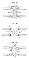
- FIGs 3A, 3B and 3C schematically illustrate three alternative mechanisms that can be used by the inventive switch to form the paths 30 and 40.
- the paths 30 and 40 are provided by parabolic reflectors.
- the path 30 is provided by the parabolic reflectors 32 and 34 which are mounted on the support 35.
- the path 40 is provided by the parabolic reflectors 42 and 44 which are also mounted on the support 35.
- the path 30 is created as follows. Light exiting from I is reflected 90 o by the parabolic reflector 32 and is collimated. The collimated radiation travels to the parabolic reflector 34. This radiation is then reflected 90 o into O.
- the path 40 is created as follows. Light exiting from Tx is reflected 90 o by the parabolic reflector 44 and is collimated. The collimated light travels to the parabolic reflector 42 and is then reflected 90 o into RX.
- FIG 3A One problem with the arrangement of FIG 3A is that if the separation between Tx and Rx and between I and O is relatively large, the collimation has to be almost perfect for the device to function. Thus, the particular mechanism of FIG 3A for providing the loop back paths 30 and 40 may not be practical in systems where the distance between Tx and Rx and the distance between I and O is on the order of 0.5 to 0.75 inches. This problem may be corrected by putting optical waveguides, such as graded index rods in between the parabolic reflectors along the paths 30 and 40. Alternatively, antireflective coatings on the reflectors.
- the paths 30 and 40 may be formed using bent optical fiber segments.
- bent optical fiber segments 36 and 46 are illustrated in FIG 3B. Relatively low loss may be achieved if the end faces of the fiber segments 36 and 46 are coated with antireflection coatings 47 and the bending radii of the fiber optic segments 36 and 46 are as large as possible. In addition, losses can be further minimized if the end faces of the fiber segments are positioned as close as possible to the end faces of Tx, Rx, I and O. This embodiment of the invention is useful when there is a relatively large spacing between Tx and Rx and between I and O such as when these separations are 0.5 or 0.75 inches.
- FIG 3C A third mechanism for providing the loop back paths 30 and 40 is shown in FIG 3C.
- the structure 50 defines two waveguides 52 and 54 each having oppositely disposed slanted end faces 55, 56 and 57, 58. Radiation from Tx reflects off the end face 57, propagates along the waveguide 54 and reflects off of end face 58 to RX. Similarly, radiation from I reflects off end face 56, propagates down the waveguide 52 and reflects off of end face 55 into O.
- the structure 50 is formed on an optical quality glass substrate.
- the waveguides 52 and 54 may be constructed by forming the beveled or slanted end faces 55, 56, 57 and 58 before or after using an ion exchange process to create the waveguide channels between the beveled end faces.
- Such waveguides are available from Corning Glass Works and Nippon Sheet Glass Co.
- a switch 100 in accordance with the present invention is schematically illustrated.
- the switch 100 In a first state, the switch 100 provides a straight throughgoing path between Tx and O and a straight throughgoing path between I and Rx.
- the switch 100 In its second state, the switch 100 provides a loop back path 40 between Tx and Rx and a loop back path 30 between I and O.
- the switch 100 comprises an assembly 102 which is mounted on a guiding means such as guide rails 104 for movement along the axis indicated by the double headed arrow 106.
- the assembly 102 is divided by a partition into two compartments 107, 108.
- the lenses 22 and 12 are located in the compartment 107 for providing the straight throughgoing paths 10, 20.
- the waveguides 52 and 54 are located in the compartment 108 for providing the loop back paths 30 and 40. (Note in some embodiments of the invention, the partition between compartments may be omitted.)
- the assembly 102 is positioned so that the compartment 107 is between Tx and Rx on one side and O and I on the opposite side.
- the node 1 is inserted into the fiber optic network (not shown in FIG 4.)
- the openings 109a, 109b show where radiation from and to I and O would enter or leave the compartment 107. Similar openings on the opposite side of the compartment 107 are provided for Tx and Rx.
- the solenoid 120 is activated.
- the magnetic field produced by the solenoid interacts with the magnet 122 to push the assembly along the rails 104 until the stop 124 is reached.
- the magnet 122 is mounted on the assembly 102 and the solenoid 120 is mounted on the support structure 123.
- the waveguides inside the compartment 108 are positioned to form the paths 30 and 40 between I and O and between Tx and Rx so that the node 1 is bypassed by the network and so that the node 1 may be tested using Rx and Tx.
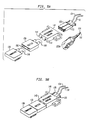
- FIGS 5A and 5B schematically illustrate an actual connection between a transceiver 130 (which comprises a transmitter and a receiver) and the incoming and outgoing optical fibers of a network.
- FIG 5A shows the components used to form the connection in unassembled condition while FIG 5B shows the components after assembly.
- the incoming and outgoing fibers form part of incoming and outgoing cables 132 and 134 respectively.
- These cables are terminated in simplex connectors 133 and 135 which are inserted into side 140 of an interconnect housing 142.
- the cables are terminated in a duplex connector 133A which is constructed for insertion into side 140 of the interconnect housing 142.
- the interconnect housing and the simplex and duplex connectors are described in U.S. Patent 4,687,291.
- the unit 150 contains the switch of the present invention.
- the unit 150 is connected by means of a duplex connector 160 to the side 144 of the interconnect housing which is opposite to the side 140.
- the transceiver unit 130 also includes a duplex connector 136 which is received in the switch 150 on a side 152 oppositely disposed from the interconnect housing 142.
- the switch of the present invention provides straight throughgoing paths between the cables 132 and 134 and transceiver 130.
- the switch provides a loop back path between the transmitter and receiver of the transceiver 130 and a loop path between the cables 132 and 134.
- the distinct switch unit 150 is eliminated and the switch is formed integrally with the interconnect housing.
Landscapes
- Physics & Mathematics (AREA)
- General Physics & Mathematics (AREA)
- Optics & Photonics (AREA)
- Mechanical Light Control Or Optical Switches (AREA)
- Optical Communication System (AREA)
Applications Claiming Priority (2)
| Application Number | Priority Date | Filing Date | Title |
|---|---|---|---|
| US221059 | 1988-07-19 | ||
| US07/221,059 US4874218A (en) | 1988-07-19 | 1988-07-19 | Reversible Optical Switch |
Publications (1)
| Publication Number | Publication Date |
|---|---|
| EP0352900A1 true EP0352900A1 (de) | 1990-01-31 |
Family
ID=22826158
Family Applications (1)
| Application Number | Title | Priority Date | Filing Date |
|---|---|---|---|
| EP89306292A Withdrawn EP0352900A1 (de) | 1988-07-19 | 1989-06-22 | Optischer Überbrückungsschalter |
Country Status (4)
| Country | Link |
|---|---|
| US (1) | US4874218A (de) |
| EP (1) | EP0352900A1 (de) |
| JP (1) | JPH0262511A (de) |
| KR (1) | KR900002094A (de) |
Cited By (2)
| Publication number | Priority date | Publication date | Assignee | Title |
|---|---|---|---|---|
| EP0503979A1 (de) * | 1991-03-15 | 1992-09-16 | The Furukawa Electric Co., Ltd. | Optischer Wellenleiter-Schalter |
| EP0661571A2 (de) * | 1993-12-29 | 1995-07-05 | AT&T Corp. | Optische Umgehungsvorrichtung |
Families Citing this family (8)
| Publication number | Priority date | Publication date | Assignee | Title |
|---|---|---|---|---|
| US4961620A (en) * | 1989-12-20 | 1990-10-09 | Raychem Corporation | Optical bypass switch |
| DE4309049C2 (de) * | 1993-03-20 | 1995-04-13 | Marquardt Gmbh | Optisches Schaltelement |
| US6832014B1 (en) * | 2002-02-08 | 2004-12-14 | Marconi Communications, Inc. | Backplane wire and noise eliminator tube |
| JP3939325B2 (ja) * | 2002-05-24 | 2007-07-04 | Hoya株式会社 | 光スイッチ及びそれを用いた光分岐挿入装置 |
| US7164817B2 (en) * | 2002-05-24 | 2007-01-16 | Hoya Corporation | Optical switch and optical add/drop multiplexer using the same |
| EP1380828B1 (de) * | 2002-07-11 | 2011-06-22 | Avago Technologies Fiber IP (Singapore) Pte. Ltd. | Optoelektronisches Modul mit integrierter Loop-back-Funktion |
| KR100626650B1 (ko) | 2003-12-27 | 2006-09-25 | 한국전자통신연구원 | 마이크로파 대역용 슬라이드식 전도체 금속 도파관 스위치 |
| US6981345B1 (en) * | 2004-06-10 | 2006-01-03 | Philip Ervin Gunn | Tool for cleaning and loading rifles |
Citations (5)
| Publication number | Priority date | Publication date | Assignee | Title |
|---|---|---|---|---|
| US4148558A (en) * | 1977-10-17 | 1979-04-10 | Ncr Corporation | Optical transmission line by-pass relay |
| EP0096615A1 (de) * | 1982-05-27 | 1983-12-21 | SOURIAU & Cie (S.A.) | Optischer Schalter |
| EP0156608A2 (de) * | 1984-03-19 | 1985-10-02 | E.I. Du Pont De Nemours And Company | Steckdose, Stecker und optischer Verbinder |
| US4715673A (en) * | 1986-05-01 | 1987-12-29 | Hitachi, Ltd. | Optical switch |
| US4736100A (en) * | 1986-07-31 | 1988-04-05 | Amp Incorporated | Optical loop attenuator simulating an optical system |
Family Cites Families (11)
| Publication number | Priority date | Publication date | Assignee | Title |
|---|---|---|---|---|
| US4401365A (en) * | 1980-02-08 | 1983-08-30 | Hitachi, Ltd. | Rotary type optical switch |
| JPS56111807A (en) * | 1980-02-08 | 1981-09-03 | Mitsubishi Electric Corp | Optical switch |
| DE3036950A1 (de) * | 1980-09-30 | 1982-05-13 | Siemens AG, 1000 Berlin und 8000 München | Faseroptischer brueckenschalter |
| JPS57186704A (en) * | 1981-05-13 | 1982-11-17 | Toshiba Corp | Optical switch |
| JPS58101536A (ja) * | 1981-12-14 | 1983-06-16 | Dainichi Nippon Cables Ltd | 環状光通信装置 |
| JPS58117504A (ja) * | 1982-01-05 | 1983-07-13 | Toshiba Corp | 光スイツチ |
| US4650278A (en) * | 1983-10-31 | 1987-03-17 | Northern Telecom Limited | Fiber optic access nodes |
| JPS6290613A (ja) * | 1985-10-17 | 1987-04-25 | Toshiba Corp | 光バイパス機構付き光伝送装置 |
| US4789215A (en) * | 1986-04-18 | 1988-12-06 | Northern Telecom Limited | Fiber optic switch with prism mounted for reciprocal and rotational movement |
| WO1988002869A1 (en) * | 1986-10-07 | 1988-04-21 | Amp Incorporated | Optical switch |
| JP2808217B2 (ja) * | 1992-08-25 | 1998-10-08 | 株式会社三井ハイテック | リードフレーム用薄板条材の熱処理方法 |
-
1988
- 1988-07-19 US US07/221,059 patent/US4874218A/en not_active Expired - Fee Related
-
1989
- 1989-06-22 EP EP89306292A patent/EP0352900A1/de not_active Withdrawn
- 1989-07-18 JP JP1185864A patent/JPH0262511A/ja active Pending
- 1989-07-19 KR KR1019890010206A patent/KR900002094A/ko not_active Application Discontinuation
Patent Citations (5)
| Publication number | Priority date | Publication date | Assignee | Title |
|---|---|---|---|---|
| US4148558A (en) * | 1977-10-17 | 1979-04-10 | Ncr Corporation | Optical transmission line by-pass relay |
| EP0096615A1 (de) * | 1982-05-27 | 1983-12-21 | SOURIAU & Cie (S.A.) | Optischer Schalter |
| EP0156608A2 (de) * | 1984-03-19 | 1985-10-02 | E.I. Du Pont De Nemours And Company | Steckdose, Stecker und optischer Verbinder |
| US4715673A (en) * | 1986-05-01 | 1987-12-29 | Hitachi, Ltd. | Optical switch |
| US4736100A (en) * | 1986-07-31 | 1988-04-05 | Amp Incorporated | Optical loop attenuator simulating an optical system |
Non-Patent Citations (3)
| Title |
|---|
| PATENT ABSTRACTS OF JAPAN, vol. 11, no. 298 (P-620)[2745], 26th September 1987, page 109 P 620; & JP-A-62 90 613 (TOSHIBA CORP.) 25-04-1987 * |
| PATENT ABSTRACTS OF JAPAN, vol. 11, no. 311 (P-625)[2758], 12th October 1987, page 71 P 625; & JP-A-62 102 219 (TOSHIBA CORP.) 12-05-1987 * |
| PATENT ABSTRACTS OF JAPAN, vol. 7, no. 204 (E-197)[1349], 9th September 1983, page 90 E 197; & JP-A-58 101 536 (DAINICHI NIPPON DENSEN K.K.) 16-06-1983 * |
Cited By (4)
| Publication number | Priority date | Publication date | Assignee | Title |
|---|---|---|---|---|
| EP0503979A1 (de) * | 1991-03-15 | 1992-09-16 | The Furukawa Electric Co., Ltd. | Optischer Wellenleiter-Schalter |
| US5177804A (en) * | 1991-03-15 | 1993-01-05 | The Furukawa Electric Co., Ltd. | Waveguide-type optical switch |
| EP0661571A2 (de) * | 1993-12-29 | 1995-07-05 | AT&T Corp. | Optische Umgehungsvorrichtung |
| EP0661571A3 (de) * | 1993-12-29 | 1996-03-20 | At & T Corp | Optische Umgehungsvorrichtung. |
Also Published As
| Publication number | Publication date |
|---|---|
| KR900002094A (ko) | 1990-02-28 |
| US4874218A (en) | 1989-10-17 |
| JPH0262511A (ja) | 1990-03-02 |
Similar Documents
| Publication | Publication Date | Title |
|---|---|---|
| US4927225A (en) | 2×2 Optical bypass switch | |
| US5757994A (en) | Three-part optical coupler | |
| US5999669A (en) | High-reliability MXN fiber optic switches | |
| US5082345A (en) | Optical fiber connecting device including attenuator | |
| US5542013A (en) | Optical fiber connector bypass device | |
| US5742712A (en) | Efficient electromechanical optical switches | |
| US6477289B1 (en) | Optical wedge switch | |
| GB2119121A (en) | Optical coupling devices | |
| US7324728B2 (en) | Optical connector with total internal reflection abutting surface | |
| US5666448A (en) | Variable splitting optical coupler | |
| AU752890B2 (en) | Multiple port, fiber optic coupling device | |
| US4874218A (en) | Reversible Optical Switch | |
| US6647173B2 (en) | Optical switch with a moveable optical component | |
| US5016966A (en) | Asymmetic optical fiber tap | |
| US11415763B2 (en) | Rigid-plane optical jumper for pluggable optical transceivers | |
| US6823102B2 (en) | Highly stable opto-mechanic switches | |
| KR940008684B1 (ko) | 광 섬유 바이패스 스위치 | |
| CN113448021B (zh) | 一种光纤连接器、单纤双向光组件及光纤传输系统 | |
| US6678438B2 (en) | Apparatus and method for switching an optical path | |
| US6591031B2 (en) | Optical switch with movable mirror | |
| US6813411B2 (en) | Optical switch | |
| US20040008924A1 (en) | Optical switch | |
| WO2001063338A1 (en) | Optical wedge switch | |
| JPH0777617A (ja) | 光導波路型光スターカプラ | |
| JPS62151042A (ja) | 光バイパス機構付き光伝送装置 |
Legal Events
| Date | Code | Title | Description |
|---|---|---|---|
| PUAI | Public reference made under article 153(3) epc to a published international application that has entered the european phase |
Free format text: ORIGINAL CODE: 0009012 |
|
| AK | Designated contracting states |
Kind code of ref document: A1 Designated state(s): DE FR GB IT |
|
| 17P | Request for examination filed |
Effective date: 19900327 |
|
| R17P | Request for examination filed (corrected) |
Effective date: 19900224 |
|
| 17Q | First examination report despatched |
Effective date: 19920414 |
|
| RAP1 | Party data changed (applicant data changed or rights of an application transferred) |
Owner name: THE WHITAKER CORPORATION |
|
| STAA | Information on the status of an ep patent application or granted ep patent |
Free format text: STATUS: THE APPLICATION IS DEEMED TO BE WITHDRAWN |
|
| 18D | Application deemed to be withdrawn |
Effective date: 19940705 |