EP0352729B1 - Feuille pour la production d'un article ayant un effet de protection contre les ondes électromagnétiques - Google Patents
Feuille pour la production d'un article ayant un effet de protection contre les ondes électromagnétiques Download PDFInfo
- Publication number
- EP0352729B1 EP0352729B1 EP19890113685 EP89113685A EP0352729B1 EP 0352729 B1 EP0352729 B1 EP 0352729B1 EP 19890113685 EP19890113685 EP 19890113685 EP 89113685 A EP89113685 A EP 89113685A EP 0352729 B1 EP0352729 B1 EP 0352729B1
- Authority
- EP
- European Patent Office
- Prior art keywords
- sheet
- synthetic resin
- layer
- forming
- metallic
- Prior art date
- Legal status (The legal status is an assumption and is not a legal conclusion. Google has not performed a legal analysis and makes no representation as to the accuracy of the status listed.)
- Expired - Lifetime
Links
- 239000010410 layer Substances 0.000 claims description 89
- 229920003002 synthetic resin Polymers 0.000 claims description 54
- 239000000057 synthetic resin Substances 0.000 claims description 54
- 239000011888 foil Substances 0.000 claims description 19
- 229920001169 thermoplastic Polymers 0.000 claims description 18
- 239000004416 thermosoftening plastic Substances 0.000 claims description 18
- 239000004831 Hot glue Substances 0.000 claims description 16
- 230000000694 effects Effects 0.000 claims description 14
- -1 polyethylene terephthalate Polymers 0.000 claims description 9
- 229920005989 resin Polymers 0.000 claims description 8
- 239000011347 resin Substances 0.000 claims description 8
- BZHJMEDXRYGGRV-UHFFFAOYSA-N Vinyl chloride Chemical compound ClC=C BZHJMEDXRYGGRV-UHFFFAOYSA-N 0.000 claims description 6
- 229920000139 polyethylene terephthalate Polymers 0.000 claims description 5
- 239000005020 polyethylene terephthalate Substances 0.000 claims description 5
- RNFJDJUURJAICM-UHFFFAOYSA-N 2,2,4,4,6,6-hexaphenoxy-1,3,5-triaza-2$l^{5},4$l^{5},6$l^{5}-triphosphacyclohexa-1,3,5-triene Chemical compound N=1P(OC=2C=CC=CC=2)(OC=2C=CC=CC=2)=NP(OC=2C=CC=CC=2)(OC=2C=CC=CC=2)=NP=1(OC=1C=CC=CC=1)OC1=CC=CC=C1 RNFJDJUURJAICM-UHFFFAOYSA-N 0.000 claims description 4
- WHHGLZMJPXIBIX-UHFFFAOYSA-N decabromodiphenyl ether Chemical compound BrC1=C(Br)C(Br)=C(Br)C(Br)=C1OC1=C(Br)C(Br)=C(Br)C(Br)=C1Br WHHGLZMJPXIBIX-UHFFFAOYSA-N 0.000 claims description 4
- 239000003063 flame retardant Substances 0.000 claims description 4
- 230000037303 wrinkles Effects 0.000 claims description 4
- YAOMHRRYSRRRKP-UHFFFAOYSA-N 1,2-dichloropropyl 2,3-dichloropropyl 3,3-dichloropropyl phosphate Chemical compound ClC(Cl)CCOP(=O)(OC(Cl)C(Cl)C)OCC(Cl)CCl YAOMHRRYSRRRKP-UHFFFAOYSA-N 0.000 claims description 2
- YSMRWXYRXBRSND-UHFFFAOYSA-N TOTP Chemical compound CC1=CC=CC=C1OP(=O)(OC=1C(=CC=CC=1)C)OC1=CC=CC=C1C YSMRWXYRXBRSND-UHFFFAOYSA-N 0.000 claims description 2
- PQYJRMFWJJONBO-UHFFFAOYSA-N Tris(2,3-dibromopropyl) phosphate Chemical compound BrCC(Br)COP(=O)(OCC(Br)CBr)OCC(Br)CBr PQYJRMFWJJONBO-UHFFFAOYSA-N 0.000 claims description 2
- 229910000410 antimony oxide Inorganic materials 0.000 claims description 2
- VTRUBDSFZJNXHI-UHFFFAOYSA-N oxoantimony Chemical compound [Sb]=O VTRUBDSFZJNXHI-UHFFFAOYSA-N 0.000 claims description 2
- 239000012188 paraffin wax Substances 0.000 claims description 2
- XZZNDPSIHUTMOC-UHFFFAOYSA-N triphenyl phosphate Chemical compound C=1C=CC=CC=1OP(OC=1C=CC=CC=1)(=O)OC1=CC=CC=C1 XZZNDPSIHUTMOC-UHFFFAOYSA-N 0.000 claims description 2
- HQUQLFOMPYWACS-UHFFFAOYSA-N tris(2-chloroethyl) phosphate Chemical compound ClCCOP(=O)(OCCCl)OCCCl HQUQLFOMPYWACS-UHFFFAOYSA-N 0.000 claims description 2
- 229920005672 polyolefin resin Polymers 0.000 claims 1
- 239000000853 adhesive Substances 0.000 description 5
- 230000001070 adhesive effect Effects 0.000 description 5
- 239000012790 adhesive layer Substances 0.000 description 5
- 239000005038 ethylene vinyl acetate Substances 0.000 description 5
- 229920001200 poly(ethylene-vinyl acetate) Polymers 0.000 description 5
- 239000004698 Polyethylene Substances 0.000 description 3
- 239000004743 Polypropylene Substances 0.000 description 3
- 239000004793 Polystyrene Substances 0.000 description 3
- 150000001336 alkenes Chemical class 0.000 description 3
- JRZJOMJEPLMPRA-UHFFFAOYSA-N olefin Natural products CCCCCCCC=C JRZJOMJEPLMPRA-UHFFFAOYSA-N 0.000 description 3
- 229920000573 polyethylene Polymers 0.000 description 3
- 238000007789 sealing Methods 0.000 description 3
- 239000000758 substrate Substances 0.000 description 3
- 229920005992 thermoplastic resin Polymers 0.000 description 3
- 238000007666 vacuum forming Methods 0.000 description 3
- RYGMFSIKBFXOCR-UHFFFAOYSA-N Copper Chemical compound [Cu] RYGMFSIKBFXOCR-UHFFFAOYSA-N 0.000 description 2
- ADCOVFLJGNWWNZ-UHFFFAOYSA-N antimony trioxide Inorganic materials O=[Sb]O[Sb]=O ADCOVFLJGNWWNZ-UHFFFAOYSA-N 0.000 description 2
- 239000007795 chemical reaction product Substances 0.000 description 2
- 238000010276 construction Methods 0.000 description 2
- 238000010438 heat treatment Methods 0.000 description 2
- 238000010030 laminating Methods 0.000 description 2
- 239000002184 metal Substances 0.000 description 2
- 229910052751 metal Inorganic materials 0.000 description 2
- 229920001155 polypropylene Polymers 0.000 description 2
- 229920002223 polystyrene Polymers 0.000 description 2
- 239000002356 single layer Substances 0.000 description 2
- YEAUATLBSVJFOY-UHFFFAOYSA-N tetraantimony hexaoxide Chemical compound O1[Sb](O2)O[Sb]3O[Sb]1O[Sb]2O3 YEAUATLBSVJFOY-UHFFFAOYSA-N 0.000 description 2
- NIXOWILDQLNWCW-UHFFFAOYSA-M Acrylate Chemical compound [O-]C(=O)C=C NIXOWILDQLNWCW-UHFFFAOYSA-M 0.000 description 1
- 229920012753 Ethylene Ionomers Polymers 0.000 description 1
- VVQNEPGJFQJSBK-UHFFFAOYSA-N Methyl methacrylate Chemical compound COC(=O)C(C)=C VVQNEPGJFQJSBK-UHFFFAOYSA-N 0.000 description 1
- 239000004721 Polyphenylene oxide Substances 0.000 description 1
- ATJFFYVFTNAWJD-UHFFFAOYSA-N Tin Chemical compound [Sn] ATJFFYVFTNAWJD-UHFFFAOYSA-N 0.000 description 1
- XECAHXYUAAWDEL-UHFFFAOYSA-N acrylonitrile butadiene styrene Chemical compound C=CC=C.C=CC#N.C=CC1=CC=CC=C1 XECAHXYUAAWDEL-UHFFFAOYSA-N 0.000 description 1
- 229920000122 acrylonitrile butadiene styrene Polymers 0.000 description 1
- 239000004676 acrylonitrile butadiene styrene Substances 0.000 description 1
- 239000004411 aluminium Substances 0.000 description 1
- 229910052782 aluminium Inorganic materials 0.000 description 1
- XAGFODPZIPBFFR-UHFFFAOYSA-N aluminium Chemical compound [Al] XAGFODPZIPBFFR-UHFFFAOYSA-N 0.000 description 1
- 239000005030 aluminium foil Substances 0.000 description 1
- 230000006399 behavior Effects 0.000 description 1
- DQXBYHZEEUGOBF-UHFFFAOYSA-N but-3-enoic acid;ethene Chemical compound C=C.OC(=O)CC=C DQXBYHZEEUGOBF-UHFFFAOYSA-N 0.000 description 1
- 239000011248 coating agent Substances 0.000 description 1
- 238000000576 coating method Methods 0.000 description 1
- 229920001577 copolymer Polymers 0.000 description 1
- 229910052802 copper Inorganic materials 0.000 description 1
- 239000010949 copper Substances 0.000 description 1
- 239000011889 copper foil Substances 0.000 description 1
- 238000005336 cracking Methods 0.000 description 1
- 238000006073 displacement reaction Methods 0.000 description 1
- 230000005684 electric field Effects 0.000 description 1
- 229920006226 ethylene-acrylic acid Polymers 0.000 description 1
- 239000000835 fiber Substances 0.000 description 1
- 238000005243 fluidization Methods 0.000 description 1
- 238000007731 hot pressing Methods 0.000 description 1
- 238000004898 kneading Methods 0.000 description 1
- 239000000463 material Substances 0.000 description 1
- 239000000203 mixture Substances 0.000 description 1
- 239000004745 nonwoven fabric Substances 0.000 description 1
- 229920000515 polycarbonate Polymers 0.000 description 1
- 239000004417 polycarbonate Substances 0.000 description 1
- 229920001225 polyester resin Polymers 0.000 description 1
- 239000004645 polyester resin Substances 0.000 description 1
- 229920006380 polyphenylene oxide Polymers 0.000 description 1
- 229920005990 polystyrene resin Polymers 0.000 description 1
- 238000001228 spectrum Methods 0.000 description 1
Images

Classifications
-
- B—PERFORMING OPERATIONS; TRANSPORTING
- B32—LAYERED PRODUCTS
- B32B—LAYERED PRODUCTS, i.e. PRODUCTS BUILT-UP OF STRATA OF FLAT OR NON-FLAT, e.g. CELLULAR OR HONEYCOMB, FORM
- B32B15/00—Layered products comprising a layer of metal
- B32B15/04—Layered products comprising a layer of metal comprising metal as the main or only constituent of a layer, which is next to another layer of the same or of a different material
- B32B15/08—Layered products comprising a layer of metal comprising metal as the main or only constituent of a layer, which is next to another layer of the same or of a different material of synthetic resin
- B32B15/09—Layered products comprising a layer of metal comprising metal as the main or only constituent of a layer, which is next to another layer of the same or of a different material of synthetic resin comprising polyesters
-
- B—PERFORMING OPERATIONS; TRANSPORTING
- B32—LAYERED PRODUCTS
- B32B—LAYERED PRODUCTS, i.e. PRODUCTS BUILT-UP OF STRATA OF FLAT OR NON-FLAT, e.g. CELLULAR OR HONEYCOMB, FORM
- B32B27/00—Layered products comprising a layer of synthetic resin
- B32B27/06—Layered products comprising a layer of synthetic resin as the main or only constituent of a layer, which is next to another layer of the same or of a different material
- B32B27/08—Layered products comprising a layer of synthetic resin as the main or only constituent of a layer, which is next to another layer of the same or of a different material of synthetic resin
-
- B—PERFORMING OPERATIONS; TRANSPORTING
- B32—LAYERED PRODUCTS
- B32B—LAYERED PRODUCTS, i.e. PRODUCTS BUILT-UP OF STRATA OF FLAT OR NON-FLAT, e.g. CELLULAR OR HONEYCOMB, FORM
- B32B27/00—Layered products comprising a layer of synthetic resin
- B32B27/30—Layered products comprising a layer of synthetic resin comprising vinyl (co)polymers; comprising acrylic (co)polymers
- B32B27/304—Layered products comprising a layer of synthetic resin comprising vinyl (co)polymers; comprising acrylic (co)polymers comprising vinyl halide (co)polymers, e.g. PVC, PVDC, PVF, PVDF
-
- B—PERFORMING OPERATIONS; TRANSPORTING
- B32—LAYERED PRODUCTS
- B32B—LAYERED PRODUCTS, i.e. PRODUCTS BUILT-UP OF STRATA OF FLAT OR NON-FLAT, e.g. CELLULAR OR HONEYCOMB, FORM
- B32B27/00—Layered products comprising a layer of synthetic resin
- B32B27/36—Layered products comprising a layer of synthetic resin comprising polyesters
-
- B—PERFORMING OPERATIONS; TRANSPORTING
- B32—LAYERED PRODUCTS
- B32B—LAYERED PRODUCTS, i.e. PRODUCTS BUILT-UP OF STRATA OF FLAT OR NON-FLAT, e.g. CELLULAR OR HONEYCOMB, FORM
- B32B3/00—Layered products comprising a layer with external or internal discontinuities or unevennesses, or a layer of non-planar shape; Layered products comprising a layer having particular features of form
- B32B3/26—Layered products comprising a layer with external or internal discontinuities or unevennesses, or a layer of non-planar shape; Layered products comprising a layer having particular features of form characterised by a particular shape of the outline of the cross-section of a continuous layer; characterised by a layer with cavities or internal voids ; characterised by an apertured layer
- B32B3/28—Layered products comprising a layer with external or internal discontinuities or unevennesses, or a layer of non-planar shape; Layered products comprising a layer having particular features of form characterised by a particular shape of the outline of the cross-section of a continuous layer; characterised by a layer with cavities or internal voids ; characterised by an apertured layer characterised by a layer comprising a deformed thin sheet, i.e. the layer having its entire thickness deformed out of the plane, e.g. corrugated, crumpled
-
- B—PERFORMING OPERATIONS; TRANSPORTING
- B32—LAYERED PRODUCTS
- B32B—LAYERED PRODUCTS, i.e. PRODUCTS BUILT-UP OF STRATA OF FLAT OR NON-FLAT, e.g. CELLULAR OR HONEYCOMB, FORM
- B32B7/00—Layered products characterised by the relation between layers; Layered products characterised by the relative orientation of features between layers, or by the relative values of a measurable parameter between layers, i.e. products comprising layers having different physical, chemical or physicochemical properties; Layered products characterised by the interconnection of layers
- B32B7/04—Interconnection of layers
- B32B7/12—Interconnection of layers using interposed adhesives or interposed materials with bonding properties
- B32B7/14—Interconnection of layers using interposed adhesives or interposed materials with bonding properties applied in spaced arrangements, e.g. in stripes
-
- H—ELECTRICITY
- H05—ELECTRIC TECHNIQUES NOT OTHERWISE PROVIDED FOR
- H05K—PRINTED CIRCUITS; CASINGS OR CONSTRUCTIONAL DETAILS OF ELECTRIC APPARATUS; MANUFACTURE OF ASSEMBLAGES OF ELECTRICAL COMPONENTS
- H05K9/00—Screening of apparatus or components against electric or magnetic fields
- H05K9/0073—Shielding materials
- H05K9/0081—Electromagnetic shielding materials, e.g. EMI, RFI shielding
- H05K9/0084—Electromagnetic shielding materials, e.g. EMI, RFI shielding comprising a single continuous metallic layer on an electrically insulating supporting structure, e.g. metal foil, film, plating coating, electro-deposition, vapour-deposition
-
- B—PERFORMING OPERATIONS; TRANSPORTING
- B32—LAYERED PRODUCTS
- B32B—LAYERED PRODUCTS, i.e. PRODUCTS BUILT-UP OF STRATA OF FLAT OR NON-FLAT, e.g. CELLULAR OR HONEYCOMB, FORM
- B32B2255/00—Coating on the layer surface
- B32B2255/10—Coating on the layer surface on synthetic resin layer or on natural or synthetic rubber layer
-
- B—PERFORMING OPERATIONS; TRANSPORTING
- B32—LAYERED PRODUCTS
- B32B—LAYERED PRODUCTS, i.e. PRODUCTS BUILT-UP OF STRATA OF FLAT OR NON-FLAT, e.g. CELLULAR OR HONEYCOMB, FORM
- B32B2255/00—Coating on the layer surface
- B32B2255/20—Inorganic coating
- B32B2255/205—Metallic coating
-
- B—PERFORMING OPERATIONS; TRANSPORTING
- B32—LAYERED PRODUCTS
- B32B—LAYERED PRODUCTS, i.e. PRODUCTS BUILT-UP OF STRATA OF FLAT OR NON-FLAT, e.g. CELLULAR OR HONEYCOMB, FORM
- B32B2307/00—Properties of the layers or laminate
- B32B2307/20—Properties of the layers or laminate having particular electrical or magnetic properties, e.g. piezoelectric
- B32B2307/212—Electromagnetic interference shielding
-
- B—PERFORMING OPERATIONS; TRANSPORTING
- B32—LAYERED PRODUCTS
- B32B—LAYERED PRODUCTS, i.e. PRODUCTS BUILT-UP OF STRATA OF FLAT OR NON-FLAT, e.g. CELLULAR OR HONEYCOMB, FORM
- B32B2327/00—Polyvinylhalogenides
- B32B2327/06—PVC, i.e. polyvinylchloride
-
- B—PERFORMING OPERATIONS; TRANSPORTING
- B32—LAYERED PRODUCTS
- B32B—LAYERED PRODUCTS, i.e. PRODUCTS BUILT-UP OF STRATA OF FLAT OR NON-FLAT, e.g. CELLULAR OR HONEYCOMB, FORM
- B32B2367/00—Polyesters, e.g. PET, i.e. polyethylene terephthalate
-
- Y—GENERAL TAGGING OF NEW TECHNOLOGICAL DEVELOPMENTS; GENERAL TAGGING OF CROSS-SECTIONAL TECHNOLOGIES SPANNING OVER SEVERAL SECTIONS OF THE IPC; TECHNICAL SUBJECTS COVERED BY FORMER USPC CROSS-REFERENCE ART COLLECTIONS [XRACs] AND DIGESTS
- Y10—TECHNICAL SUBJECTS COVERED BY FORMER USPC
- Y10S—TECHNICAL SUBJECTS COVERED BY FORMER USPC CROSS-REFERENCE ART COLLECTIONS [XRACs] AND DIGESTS
- Y10S428/00—Stock material or miscellaneous articles
- Y10S428/92—Fire or heat protection feature
- Y10S428/921—Fire or flameproofing
-
- Y—GENERAL TAGGING OF NEW TECHNOLOGICAL DEVELOPMENTS; GENERAL TAGGING OF CROSS-SECTIONAL TECHNOLOGIES SPANNING OVER SEVERAL SECTIONS OF THE IPC; TECHNICAL SUBJECTS COVERED BY FORMER USPC CROSS-REFERENCE ART COLLECTIONS [XRACs] AND DIGESTS
- Y10—TECHNICAL SUBJECTS COVERED BY FORMER USPC
- Y10T—TECHNICAL SUBJECTS COVERED BY FORMER US CLASSIFICATION
- Y10T428/00—Stock material or miscellaneous articles
- Y10T428/24—Structurally defined web or sheet [e.g., overall dimension, etc.]
- Y10T428/24479—Structurally defined web or sheet [e.g., overall dimension, etc.] including variation in thickness
- Y10T428/24562—Interlaminar spaces
-
- Y—GENERAL TAGGING OF NEW TECHNOLOGICAL DEVELOPMENTS; GENERAL TAGGING OF CROSS-SECTIONAL TECHNOLOGIES SPANNING OVER SEVERAL SECTIONS OF THE IPC; TECHNICAL SUBJECTS COVERED BY FORMER USPC CROSS-REFERENCE ART COLLECTIONS [XRACs] AND DIGESTS
- Y10—TECHNICAL SUBJECTS COVERED BY FORMER USPC
- Y10T—TECHNICAL SUBJECTS COVERED BY FORMER US CLASSIFICATION
- Y10T428/00—Stock material or miscellaneous articles
- Y10T428/24—Structurally defined web or sheet [e.g., overall dimension, etc.]
- Y10T428/24479—Structurally defined web or sheet [e.g., overall dimension, etc.] including variation in thickness
- Y10T428/2457—Parallel ribs and/or grooves
-
- Y—GENERAL TAGGING OF NEW TECHNOLOGICAL DEVELOPMENTS; GENERAL TAGGING OF CROSS-SECTIONAL TECHNOLOGIES SPANNING OVER SEVERAL SECTIONS OF THE IPC; TECHNICAL SUBJECTS COVERED BY FORMER USPC CROSS-REFERENCE ART COLLECTIONS [XRACs] AND DIGESTS
- Y10—TECHNICAL SUBJECTS COVERED BY FORMER USPC
- Y10T—TECHNICAL SUBJECTS COVERED BY FORMER US CLASSIFICATION
- Y10T428/00—Stock material or miscellaneous articles
- Y10T428/24—Structurally defined web or sheet [e.g., overall dimension, etc.]
- Y10T428/24628—Nonplanar uniform thickness material
- Y10T428/24661—Forming, or cooperating to form cells
-
- Y—GENERAL TAGGING OF NEW TECHNOLOGICAL DEVELOPMENTS; GENERAL TAGGING OF CROSS-SECTIONAL TECHNOLOGIES SPANNING OVER SEVERAL SECTIONS OF THE IPC; TECHNICAL SUBJECTS COVERED BY FORMER USPC CROSS-REFERENCE ART COLLECTIONS [XRACs] AND DIGESTS
- Y10—TECHNICAL SUBJECTS COVERED BY FORMER USPC
- Y10T—TECHNICAL SUBJECTS COVERED BY FORMER US CLASSIFICATION
- Y10T428/00—Stock material or miscellaneous articles
- Y10T428/24—Structurally defined web or sheet [e.g., overall dimension, etc.]
- Y10T428/24628—Nonplanar uniform thickness material
- Y10T428/24669—Aligned or parallel nonplanarities
- Y10T428/24694—Parallel corrugations
- Y10T428/24711—Plural corrugated components
-
- Y—GENERAL TAGGING OF NEW TECHNOLOGICAL DEVELOPMENTS; GENERAL TAGGING OF CROSS-SECTIONAL TECHNOLOGIES SPANNING OVER SEVERAL SECTIONS OF THE IPC; TECHNICAL SUBJECTS COVERED BY FORMER USPC CROSS-REFERENCE ART COLLECTIONS [XRACs] AND DIGESTS
- Y10—TECHNICAL SUBJECTS COVERED BY FORMER USPC
- Y10T—TECHNICAL SUBJECTS COVERED BY FORMER US CLASSIFICATION
- Y10T428/00—Stock material or miscellaneous articles
- Y10T428/24—Structurally defined web or sheet [e.g., overall dimension, etc.]
- Y10T428/24802—Discontinuous or differential coating, impregnation or bond [e.g., artwork, printing, retouched photograph, etc.]
- Y10T428/24826—Spot bonds connect components
-
- Y—GENERAL TAGGING OF NEW TECHNOLOGICAL DEVELOPMENTS; GENERAL TAGGING OF CROSS-SECTIONAL TECHNOLOGIES SPANNING OVER SEVERAL SECTIONS OF THE IPC; TECHNICAL SUBJECTS COVERED BY FORMER USPC CROSS-REFERENCE ART COLLECTIONS [XRACs] AND DIGESTS
- Y10—TECHNICAL SUBJECTS COVERED BY FORMER USPC
- Y10T—TECHNICAL SUBJECTS COVERED BY FORMER US CLASSIFICATION
- Y10T428/00—Stock material or miscellaneous articles
- Y10T428/24—Structurally defined web or sheet [e.g., overall dimension, etc.]
- Y10T428/24802—Discontinuous or differential coating, impregnation or bond [e.g., artwork, printing, retouched photograph, etc.]
- Y10T428/24851—Intermediate layer is discontinuous or differential
-
- Y—GENERAL TAGGING OF NEW TECHNOLOGICAL DEVELOPMENTS; GENERAL TAGGING OF CROSS-SECTIONAL TECHNOLOGIES SPANNING OVER SEVERAL SECTIONS OF THE IPC; TECHNICAL SUBJECTS COVERED BY FORMER USPC CROSS-REFERENCE ART COLLECTIONS [XRACs] AND DIGESTS
- Y10—TECHNICAL SUBJECTS COVERED BY FORMER USPC
- Y10T—TECHNICAL SUBJECTS COVERED BY FORMER US CLASSIFICATION
- Y10T428/00—Stock material or miscellaneous articles
- Y10T428/24—Structurally defined web or sheet [e.g., overall dimension, etc.]
- Y10T428/24802—Discontinuous or differential coating, impregnation or bond [e.g., artwork, printing, retouched photograph, etc.]
- Y10T428/24917—Discontinuous or differential coating, impregnation or bond [e.g., artwork, printing, retouched photograph, etc.] including metal layer
-
- Y—GENERAL TAGGING OF NEW TECHNOLOGICAL DEVELOPMENTS; GENERAL TAGGING OF CROSS-SECTIONAL TECHNOLOGIES SPANNING OVER SEVERAL SECTIONS OF THE IPC; TECHNICAL SUBJECTS COVERED BY FORMER USPC CROSS-REFERENCE ART COLLECTIONS [XRACs] AND DIGESTS
- Y10—TECHNICAL SUBJECTS COVERED BY FORMER USPC
- Y10T—TECHNICAL SUBJECTS COVERED BY FORMER US CLASSIFICATION
- Y10T428/00—Stock material or miscellaneous articles
- Y10T428/24—Structurally defined web or sheet [e.g., overall dimension, etc.]
- Y10T428/24942—Structurally defined web or sheet [e.g., overall dimension, etc.] including components having same physical characteristic in differing degree
- Y10T428/2495—Thickness [relative or absolute]
- Y10T428/24959—Thickness [relative or absolute] of adhesive layers
-
- Y—GENERAL TAGGING OF NEW TECHNOLOGICAL DEVELOPMENTS; GENERAL TAGGING OF CROSS-SECTIONAL TECHNOLOGIES SPANNING OVER SEVERAL SECTIONS OF THE IPC; TECHNICAL SUBJECTS COVERED BY FORMER USPC CROSS-REFERENCE ART COLLECTIONS [XRACs] AND DIGESTS
- Y10—TECHNICAL SUBJECTS COVERED BY FORMER USPC
- Y10T—TECHNICAL SUBJECTS COVERED BY FORMER US CLASSIFICATION
- Y10T428/00—Stock material or miscellaneous articles
- Y10T428/24—Structurally defined web or sheet [e.g., overall dimension, etc.]
- Y10T428/24942—Structurally defined web or sheet [e.g., overall dimension, etc.] including components having same physical characteristic in differing degree
- Y10T428/2495—Thickness [relative or absolute]
- Y10T428/24967—Absolute thicknesses specified
-
- Y—GENERAL TAGGING OF NEW TECHNOLOGICAL DEVELOPMENTS; GENERAL TAGGING OF CROSS-SECTIONAL TECHNOLOGIES SPANNING OVER SEVERAL SECTIONS OF THE IPC; TECHNICAL SUBJECTS COVERED BY FORMER USPC CROSS-REFERENCE ART COLLECTIONS [XRACs] AND DIGESTS
- Y10—TECHNICAL SUBJECTS COVERED BY FORMER USPC
- Y10T—TECHNICAL SUBJECTS COVERED BY FORMER US CLASSIFICATION
- Y10T428/00—Stock material or miscellaneous articles
- Y10T428/31504—Composite [nonstructural laminate]
- Y10T428/31678—Of metal
- Y10T428/31681—Next to polyester, polyamide or polyimide [e.g., alkyd, glue, or nylon, etc.]
-
- Y—GENERAL TAGGING OF NEW TECHNOLOGICAL DEVELOPMENTS; GENERAL TAGGING OF CROSS-SECTIONAL TECHNOLOGIES SPANNING OVER SEVERAL SECTIONS OF THE IPC; TECHNICAL SUBJECTS COVERED BY FORMER USPC CROSS-REFERENCE ART COLLECTIONS [XRACs] AND DIGESTS
- Y10—TECHNICAL SUBJECTS COVERED BY FORMER USPC
- Y10T—TECHNICAL SUBJECTS COVERED BY FORMER US CLASSIFICATION
- Y10T428/00—Stock material or miscellaneous articles
- Y10T428/31504—Composite [nonstructural laminate]
- Y10T428/31678—Of metal
- Y10T428/31692—Next to addition polymer from unsaturated monomers
- Y10T428/31699—Ester, halide or nitrile of addition polymer
Definitions
- the present invention relates to a forming sheet having a high shielding effect against electromagnetic interference (hereinafter referred to as EMI), e.g. for forming a housing of an electronic device, said forming sheet being suitable for forming such an article by vacuum forming or pressure forming.
- EMI electromagnetic interference
- a forming sheet used to be formed into an article having a high shielding effect against EMI such as a housing of an electronic device is also required to have a good electrical conductivity.
- a sheet has heretofore been made by kneading metal in the form of fiber or flakes into a thermoplastic resin so as to be uniformly dispersed in the resin or by laminating a thermoplastic resin and a conductive non-woven fabric together.
- EP-A-0 220 720 disloses a laminate wherein a heat-shrinkable resin and a metal foil are bonded by a discontinuous bonding layer formed by a synthetic resin layer applied at intervals and an adhesive layer covering the whole surface thereof. A further thermoplastic resin layer can be applied to the laminate using an adhesive.
- Another object of the present invention is to provide an article formed from such a forming sheet which has a good shielding effect as well as a good flame resistance.
- a forming sheet having a shielding effect against electromagnetic interference comprising the features of claim 1.
- thermoplastic synthetic resin sheet may be provided on either one or both side of the conductive laminated sheet.
- the forming sheet according to the present invention has an improved flame resistance by admixing a flame retardant to the hot melt adhesive layer.
- the conductive laminated sheet has an electrical conductivity owing to the provision of the metallic layer.
- the metallic layer will develop a multiplicity of fine wrinkles as a result of shrinkage of the heat-shrinkable synthetic resin.
- the conductive laminated sheet When forming such a sheet into an article, the conductive laminated sheet will be subjected to stretching. But the metallic layer forming the conductive layer will be protected against tear because the wrinkles formed thereon beforehand absorb elongation.
- the conductive laminated sheet and the thermoplastic synthetic resin sheet are elongated to different degrees from each other during the forming, such a difference in elongation will be absorbed by the fluidization of the hot melt adhesive layer by heat during forming.
- the article thus formed will have a good appearance.
- the thermoplastic synthetic resin sheet may be made of a vinyl chloride resin and the hot melt adhesive layer having flame resistance may be used. Thus, no peeling will take place between the conductive laminated sheet and the thermoplastic synthetic resin sheet when the forming sheet is burnt. As a result, the forming sheet has a good flame resistance as a whole.
- the synthetic resin should preferably be polyethylene terephthalate which has a good heat resistance.
- the elongation of the metallic film during forming is reduced to a minimum, thus preventing the layer from cracking. This will assure high shielding effect against EMI without causing any crack in the metallic layer.
- the conductive laminated sheet is made of a metallic film comprising a synthetic resin layer provided with a metallized layer and a metallic foil laminated thereto or is provided in two or more layers.
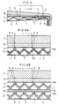
- the forming sheet according to the present invention comprises a conductive laminated sheet A, a hot melt adhesive layer B and a thermoplastic synthetic resin sheet C. (Fig. 4)
- the conductive laminated sheet A is made by heating to shrink a substrate 5 including a metallic film 1 and a heat-shrinkable synthetic resin film 4 laminated to both sides or one side of the metallic film 1 through a discontinuous bonding layer 3 as shown in Figs. 1a and 1b, respectively.
- Fig. 2b shows a metallic film 1 having a metallized layer Mb or a metallic foil layer Ma formed on both sides of the synthetic resin layer 2.
- Fig. 2c shows a metallic film 1 having the layer Mb or Ma formed on one side of the synthetic resin layer 2.
- the metallic film 1 may be a laminate having the synthetic resin layer 2, the metallized layer Mb, and the metallic foil Ma.
- Figs. 2d shows an example in which the metallic foil Ma is laminated to one side of the synthetic resin layer 2 and the metallized layer Mb is formed on the other side thereof.
- Fig. 2e shows another example in which the metallized layer Mb is formed on one side of the synthetic resin layer 2 and the metallic foil Ma is further laminated to the metallized layer Mb.
- the metallic film 1 has the metallized layers Mb formed on both sides of the synthetic resin layer 2 and the metallic foil Ma is laminated to one of the metallized layers Mb.
- Figs. 1a and 1b show two different kinds of substrates 5 before being subjected to heat shrinkage and Fig. 3 shows the substrate of Fig. 1a after subjected to heat shrinkage.
- the metallic layer forming the metallic film 1 may be a metallic foil such as an aluminium foil or a copper foil or a metallized layer of aluminium or tin.
- the total thickness of the metallic layer or layers should be not less than 0.02 micron so that they can effectively shield EMI after forming and should preferably be more than 0.1 micron. But it should not be more than 15 microns from an economical viewpoint.
- the synthetic resin layer 2 forming the metallic film 1 may be of a single-layer or a multi-layer construction and should be made of polyethylene, polypropylene, vinyl chloride, polystyrene, acrylate, polyethylene terephthalate (abbreviated to PET in the Table) or ethylene-vinyl acetate copolymer. Polyethylene terephthalate which has a high heat resistance is the most preferable.
- the thickness of the synthetic rsein layer should be 4 to 25 microns.
- the metallic film 1 may be made either by coating the synthetic resin layer 2 on the metallic layers or by laminating the resin layer to the metallic layer if the metallic layer is a metallic foil. If it is a metallized layer, the synthetic resin layer 2 may be metallized.
- the heat-shrinkable synthetic resin film 4 should preferably be made of a resin selected from polyethylene, polypropylene (abbreviated to PP in the Table), vinyl chloride, polystyrene and polyester resins and having as large a shrinkage ratio as possible (e.g. 50 per cent). It may be of a single-layer construction or a laminate of two or more films.
- the discontinuous bonding layer 3 should be of any adhesive material capable of bonding the metallic film 1 and the heat-shrinkable synthetic resin film 4 together. Also, they may be bonded together discontinuously by heat sealing or ultrasonic sealing.
- the discontinuous bonding layer 3 may have a linear, dotted, lattice or any other pattern, as viewed from top, so long as it is not present over the entire interface between the metallic film 1 and the synthetic resin films 4 but is formed so as to leave voids 6.
- the hot melt adhesive layer B should be made of an olefin adhesive or a mixture of olefin adhesives such as ethylene-vinyl acetate (abbreviated to EVA in the Table), ethylene-acrylic acid ester copolymer, ethylene ionomer, and polyethylene.
- EVA ethylene-vinyl acetate
- At least one flame retardant selected from the group consisting of tricresyl phosphate, tris (chloroethyl) phosphate, tris (dichloropropyl) phosphate, tris (dibromopropyl) phosphate, triphenyl phosphate, decabromodiphenyl ether, chlorinated paraffin and antimony oxide may be mixed into the olefin adhesives.
- the content of the flame retardant in the hot melt adhesive layer B should be 20 - 70 per cent by weight, preferably 40 - 60 per cent by weight. If less than 20 per cent, the flame retardance will be insufficient. If more than 70 per cent, the cost will be too high.
- the layer B should have a thickness of 30 - 200 microns, preferably 50 - 150 microns. If less than 30 microns, it cannot damp the stress owing to any displacement during forming. If more than 200 microns, the cost will be too high.
- thermoplastic synthetic resin sheet C should be made of a vinyl chloride, methyl methacrylate, acrylonitrile-butadiene-styrene, polystyrene, polycarbonate or modified polyphenylene oxide resin.
- thermoplastic synthetic resin sheet C should preferably be made of a vinyl chloride resin having an excellent flame resistance. Its thickness is normally 3.0 to 5.0 mm, but not limited thereto.
- the conductive laminated sheet A, the hot melt adhesive layer B and the thermoplastic synthetic resin sheet C may be laminated together by various means.
- the conductive laminated sheet A may be continuously laminated thereon through the hot melt adhesive layer B.
- the conductive laminated sheet A, the hot melt adhesive layer B and the thermoplastic synthetic resin sheet C may be put one upon another and laminated together by hot pressing.
- the forming sheet thus made may be formed while heating by vacuum forming or pressure forming so that the thermoplastic synthetic resin layer C will serve as the working surface of the formed article.
- the conductive laminated sheet A is bonded to the thermoplastic synthetic resin sheet C through the hot melt adhesive layer B.
- the rate of elongation of the thermoplastic synthetic resin sheet C during forming is larger than that of the conductive laminated sheet A because the latter is formed by heat-shrinkage.
- the difference in elongation is especially remarkable at the corners and the uprising portions of the forming mold.
- the points a-a and b-b in Fig. 4 before forming will move to the points a′-a′ and b′-b′ in Fig. 5, respectively, after forming.
- the distances L between points a-a and between points b-b will increase to La′ and Lb′, respectively.
- the hot melt adhesive layer B is heated and fluidized.
- the metallic film 1 of the conductive laminated sheet A is made of a synthetic resin layer 2 having a metallic foil Ma formed on its side facing the thermoplastic synthetic resin sheet C and a metallized layer Mb formed on the other side.
- the formed piece formed from this sheet had a good appearance and high shielding effect against EMI.
- two conductive laminated sheets A′ and A ⁇ are laminated together after subjecting them to heat shrinkage.
- the former sheet A′ comprises a metallic film 1 which is a metallic foil Ma, and a heat-shrinkable synthetic resin film 4 laminated to both sides of the metallic foil Ma through discontinuous bonding layers 3, and the latter sheet A ⁇ comprises a metallic film 1 having a synthetic resin layer 2 and a metallized layer Mb formed on at least one side thereof, and heat-shrinkable synthetic resin films 4 laminated to both sides of the metallic film 1 through discontinuous bonding layers 3.
- the sheet A′ may be laminated to the synthetic resin sheet C through the adhesive layer B, after laminated to the sheet A ⁇ .
- the conductive laminated sheets A′ and A ⁇ may be bonded together by sealing their heat-shrinkable synthetic resin films 4 together or bonding through a hot melt adhesive layer B′ similar to the adhesive layer B.
- Tables 1 and 2 show the structure and the test results of the embodiments 1 - 7 according to the present invention and the comparison examples 1 to 5 prepared for comparison purposes.
- the articles formed from the sheets in embodiments 1 - 3 had a good appearance on both sides. Neither breakage nor peeling of their metallic film was observed even at the corner portions on the back side.
- the formed article in the embodiments 5 and 6 each including a hot melt adhesive layer B composed of EVA (MI 0.8 g/10 min, VA cont 20 %) 40 per cent by weight Decabromodiphenyl ether 24 " Sb2O3 36 " were also found out to clear the UL 94 V-0.
- the comparison example 2 achieved a satisfactory result in formability. But the end product failed to reveal a sufficient shielding effect against EMI. Moreover, peeling was observed between the sheets A and C during a burning test and its flame resistance was so poor that it meets the requirements corresponding to only the UL 94 HB.
- the EMI shielding effect of each formed article was determined by measuring the attenuation (in dB) in an electric field of 30 to 1000 MHz produced by a transmitter mounted in a copper cabinet on one side of which the article was mounted.
- the attenuation was measured by use of a receiving antenna provided at a distance of 3 meters from the transmitter, and a spectrum analyzer.
Landscapes
- Physics & Mathematics (AREA)
- Electromagnetism (AREA)
- Engineering & Computer Science (AREA)
- Microelectronics & Electronic Packaging (AREA)
- Laminated Bodies (AREA)
Claims (8)
- Feuille de conformation ayant un effet d'écran contre les interférences électromagnétiques, comprenant une feuille stratifiée conductrice (A) et une feuille en résine synthétique thermoplastique (C) contrecollée sur au moins un côté de ladite feuille stratifiée conductrice par l'intermédiaire d'une couche adhésive fondue chaude (B) ayant une épaisseur de 30 à 200 »m, ladite couche stratifiée conductrice comprenant une pellicule métallique présentant de multiples plis fins et une pellicule en résine synthétique thermorétractée (4) contrecollée sur au moins un côté de ladite pellicule métallique (1) par l'intermédiaire d'une couche de liaison discontinue (3) laissant des vides (6) entre la pellicule métallique (1) et la pellicule en résine synthétique (4).
- Feuille de conformation selon la revendication 1, dans laquelle pellicule métallique comprend une couche en résine synthétique (2) et une couche métallisée (Mb) formée sur au moins un côté de ladite couche en résine synthétique, ladite couche métallisée ayant une épaisseur de 0,02 à 3 »m.
- Feuille de conformation selon la revendication 1, dans laquelle pellicule métallique est une feuille métallique (Ma) ayant une épaisseur de 3 à 15 »m.
- Feuille de conformation selon la revendication 1, dans laquelle pellicule métallique comprend une couche en résine synthétique (2), et une couche métallisée (Mb) formée sur au moins un côté de ladite couche en résine synthétique et ayant une épaisseur de 0,02 à 3 »m, et une feuille métallique (Ma) ayant une épaisseur de 3 à 15 »m.
- Feuille de conformation selon la revendication 1, dans laquelle ladite feuille stratifiée conductrice est constituée de deux couches ou plus.
- Feuille de conformation selon la revendication 2 ou 4, dans laquelle ladite couche en résine synthétique (2) est constituée de polyéthylène téréphtalate.
- Feuille de conformation selon la revendication 1, dans laquelle ladite couche adhésive fondue chaude (B) est constituée d'une résine polyoléfine et contient 20 à 70 % en poids d'au moins un retardateur de flamme choisi dans le groupe composé des phosphate de tricrésyle, phosphate de tris(chloroéthyle), phosphate de tris(dichloropropyle), phosphate de tris(dibromopropyle), phosphate de triphényle, décabromodiphényléther, paraffine chlorée et oxyde d'antimoine.
- Feuille de conformation selon la revendication 1, dans laquelle ladite feuille en résine synthétique thermoplastique (C) est une résine de chlorure de vinyle.
Applications Claiming Priority (4)
| Application Number | Priority Date | Filing Date | Title |
|---|---|---|---|
| JP18937588 | 1988-07-27 | ||
| JP189375/88 | 1988-07-27 | ||
| JP106298/89 | 1989-04-25 | ||
| JP1106298A JP2641561B2 (ja) | 1988-07-27 | 1989-04-25 | 電磁波シールド性を有する成形用シート及びそのシートを用いた成形体 |
Publications (3)
| Publication Number | Publication Date |
|---|---|
| EP0352729A2 EP0352729A2 (fr) | 1990-01-31 |
| EP0352729A3 EP0352729A3 (en) | 1990-07-25 |
| EP0352729B1 true EP0352729B1 (fr) | 1994-07-13 |
Family
ID=26446420
Family Applications (1)
| Application Number | Title | Priority Date | Filing Date |
|---|---|---|---|
| EP19890113685 Expired - Lifetime EP0352729B1 (fr) | 1988-07-27 | 1989-07-25 | Feuille pour la production d'un article ayant un effet de protection contre les ondes électromagnétiques |
Country Status (3)
| Country | Link |
|---|---|
| US (1) | US4980223A (fr) |
| EP (1) | EP0352729B1 (fr) |
| DE (1) | DE68916716T2 (fr) |
Families Citing this family (42)
| Publication number | Priority date | Publication date | Assignee | Title |
|---|---|---|---|---|
| JPH02103808A (ja) * | 1988-10-12 | 1990-04-16 | Kitagawa Kogyo Kk | 帯状ケーブル |
| US5286318A (en) * | 1990-04-04 | 1994-02-15 | The Curran Company | Method of forming EMI shielded enclosures, EMI shielded enclosures and EMI shields |
| DE4016953A1 (de) * | 1990-05-25 | 1991-11-28 | Itt Ind Gmbh Deutsche | Elektronisches bauelement mit abschirmung gegen elektromagnetische stoerstrahlung und verfahren zur herstellung |
| KR930006305B1 (ko) * | 1991-07-09 | 1993-07-12 | 한국과학기술연구원 | 텅스텐 박막 제조용 플라즈마 화학증착 온도 측정장치 |
| US5443900A (en) * | 1991-09-10 | 1995-08-22 | Kansai Paint Co., Ltd. | Electromagnetic wave absorber |
| US5401901A (en) * | 1991-09-19 | 1995-03-28 | W. L. Gore & Associates, Inc. | Weather-resistant electromagnetic interference shielding for electronic equipment enclosures |
| US5723223A (en) * | 1991-10-07 | 1998-03-03 | International Paper Company | Ultrasonically bonded microwave susceptor material and method for its manufacture |
| JP2647589B2 (ja) * | 1992-01-27 | 1997-08-27 | 矢崎総業株式会社 | 電磁波遮蔽用複合シート |
| US5318855A (en) * | 1992-08-25 | 1994-06-07 | International Business Machines Corporation | Electronic assembly with flexible film cover for providing electrical and environmental protection |
| US5477421A (en) * | 1993-11-18 | 1995-12-19 | Itt Corporation | Shielded IC card |
| US5477426A (en) * | 1993-12-15 | 1995-12-19 | Itt Corporation | IC card with board positioning means |
| US5563770A (en) * | 1994-02-25 | 1996-10-08 | Itt Corporation | IC card with board positioning means |
| EP0658678A1 (fr) * | 1993-12-17 | 1995-06-21 | Hermann Forster Ag | Eléments de fenêtre protectrice |
| US5581049A (en) * | 1994-04-13 | 1996-12-03 | Orion Industries Incorporated | Expanding joint for an initially substantially planar member |
| US5817973A (en) * | 1995-06-12 | 1998-10-06 | Berg Technology, Inc. | Low cross talk and impedance controlled electrical cable assembly |
| GB9523002D0 (en) * | 1995-11-09 | 1996-01-10 | Raychem Ltd | Flame-retarded adhesive composition |
| CA2197728A1 (fr) * | 1996-03-25 | 1997-09-25 | William Roger Lambert | Methode pour donner des proprietes de protection electromagnetique et de barriere de diffusion de l'extrusion de plastique et dispositifs fabriques a partir de cette methode |
| EP0883156B9 (fr) * | 1997-06-03 | 2005-09-21 | Hitachi Chemical Co., Ltd. | Pellicule adhésive à blindage électromagnétique |
| US6455770B2 (en) | 1997-07-03 | 2002-09-24 | Lee J. Pulver | Electromagnetic radiation shield for attenuating electromagnetic radiation from an active electronic device |
| US6476317B1 (en) * | 1997-07-15 | 2002-11-05 | The United States Of America As Represented By The Secretary Of The Air Force | Radiation shield using electrical insulating materials and the spacecharge fields therein |
| US6086979A (en) | 1997-11-11 | 2000-07-11 | Hitachi Chemical Company, Ltd. | Electromagnetically shielding bonding film, and shielding assembly and display device using such film |
| DE69924421T2 (de) * | 1998-01-30 | 2006-03-09 | Toyo Boseki K.K. | Wärmeschrumpfbarer Polyesterfilm |
| AU3357599A (en) * | 1998-03-18 | 1999-10-11 | Ntk Powerdex, Inc. | Packaging material for hermetically sealed batteries |
| US6188015B1 (en) * | 1998-06-02 | 2001-02-13 | The Curran Company | Electromagnetic interference attenuation device |
| US6593524B1 (en) | 2000-06-15 | 2003-07-15 | Thomas Toedtman | Device and method for providing EMI/RFI shielding |
| US7207744B2 (en) * | 2001-02-28 | 2007-04-24 | Owens Corning Fiberglas Technology, Inc. | Mats for use in paved surfaces |
| US8043025B2 (en) * | 2001-02-28 | 2011-10-25 | Owens Corning Intellectual Capital, Llc | Mats for use in paved surfaces |
| JP4193396B2 (ja) * | 2002-02-08 | 2008-12-10 | 住友電気工業株式会社 | 伝送用メタルケーブル |
| US20050135727A1 (en) * | 2003-12-18 | 2005-06-23 | Sioptical, Inc. | EMI-EMC shield for silicon-based optical transceiver |
| US8545974B2 (en) * | 2005-02-09 | 2013-10-01 | Laird Technologies, Inc. | Flame retardant EMI shields |
| US20100258344A1 (en) * | 2005-02-09 | 2010-10-14 | Laird Technologies, Inc. | Flame retardant emi shields |
| US9746230B2 (en) * | 2006-02-24 | 2017-08-29 | Carrier Corporation | Flame retardant door for transport refrigeration unit |
| JP5257180B2 (ja) * | 2008-11-19 | 2013-08-07 | 住友電装株式会社 | 電線の保護材 |
| JP2011067771A (ja) * | 2009-09-25 | 2011-04-07 | Panasonic Electric Works Co Ltd | 放電装置 |
| DE102010019837A1 (de) * | 2010-05-08 | 2011-11-10 | Dietmar G. Turnau | Abhörschutztasche für Drahtlos-Kommunikationsgerät als Mittel gegen Fremdmanipulation und Bespitzelung zur zeitweiligen Nutzung während vertraulicher Besprechungen |
| US9322164B2 (en) | 2010-08-19 | 2016-04-26 | Sealed Air Corporation (Us) | Multilayer air-cellular insulation laminate containing two-side metallized film |
| US8691393B2 (en) * | 2010-10-27 | 2014-04-08 | Laird Technologies, Inc. | EMI shielding heat shrinkable tapes |
| WO2012057746A1 (fr) * | 2010-10-27 | 2012-05-03 | Laird Technologies, Inc. | Bandes thermorétractables de blindage contre les interférences électromagnétiques |
| JP5041495B2 (ja) * | 2010-11-01 | 2012-10-03 | シャープ株式会社 | イオン発生装置 |
| JP5675329B2 (ja) * | 2010-12-27 | 2015-02-25 | 矢崎総業株式会社 | 導電路シールド構造、及び、ワイヤハーネス |
| US9766662B2 (en) * | 2015-04-22 | 2017-09-19 | Apple Inc. | Conductive gasket for a portable computing device |
| CN111431239A (zh) * | 2020-04-20 | 2020-07-17 | 蓝沛光线(上海)电子科技有限公司 | 一种无线充电模组及其制备方法 |
Family Cites Families (7)
| Publication number | Priority date | Publication date | Assignee | Title |
|---|---|---|---|---|
| JPS5112856B1 (fr) * | 1967-05-09 | 1976-04-22 | ||
| US3754094A (en) * | 1971-01-25 | 1973-08-21 | Kabel Metallwerke Ghh | Cable with welded corrugated metal sheath |
| US4678699A (en) * | 1982-10-25 | 1987-07-07 | Allied Corporation | Stampable polymeric composite containing an EMI/RFI shielding layer |
| US4647714A (en) * | 1984-12-28 | 1987-03-03 | Sohwa Laminate Printing Co., Ltd. | Composite sheet material for magnetic and electronic shielding and product obtained therefrom |
| US4767673A (en) * | 1985-10-28 | 1988-08-30 | Toyo Aluminium Kabushiki Kaisha | Laminates and formings made from the same |
| US4654755A (en) * | 1986-03-03 | 1987-03-31 | Motorola, Inc. | Microwave/millimeter wave ground plane |
| US4749625A (en) * | 1986-03-31 | 1988-06-07 | Hiraoka & Co., Ltd. | Amorphous metal laminate sheet |
-
1989
- 1989-07-25 EP EP19890113685 patent/EP0352729B1/fr not_active Expired - Lifetime
- 1989-07-25 US US07/384,591 patent/US4980223A/en not_active Expired - Fee Related
- 1989-07-25 DE DE1989616716 patent/DE68916716T2/de not_active Expired - Fee Related
Also Published As
| Publication number | Publication date |
|---|---|
| DE68916716D1 (de) | 1994-08-18 |
| EP0352729A2 (fr) | 1990-01-31 |
| EP0352729A3 (en) | 1990-07-25 |
| DE68916716T2 (de) | 1995-03-02 |
| US4980223A (en) | 1990-12-25 |
Similar Documents
| Publication | Publication Date | Title |
|---|---|---|
| EP0352729B1 (fr) | Feuille pour la production d'un article ayant un effet de protection contre les ondes électromagnétiques | |
| JP2755479B2 (ja) | 帯電防止シート材料、包装体及び製造方法 | |
| US4965408A (en) | Composite sheet material for electromagnetic radiation shielding | |
| US4677809A (en) | Method of making packing material with anti-static coating | |
| KR100950818B1 (ko) | 난연제 전자파 차폐재료 | |
| US5595801A (en) | Laminated shielding material and method for shielding an enclosure therewith | |
| US4415946A (en) | Antistatic chairmat | |
| JPH0458786B2 (fr) | ||
| KR101810784B1 (ko) | 탄소섬유 발열보드 및 그 제조방법 | |
| EP0350056B1 (fr) | Feuille thermoplastique électroconductrice et objets moulés | |
| US4875581A (en) | Static dissipative elastomeric coating for electronic packaging components | |
| KR20140113507A (ko) | 난연성, 전기 도전성 접착 재료 및 관련 방법 | |
| EP0119780A2 (fr) | Laminé protecteur contre les interférences électroniques | |
| US4472474A (en) | Electrically conductive laminate | |
| JP2641561B2 (ja) | 電磁波シールド性を有する成形用シート及びそのシートを用いた成形体 | |
| JP3593747B2 (ja) | フラットケーブルおよび製造方法 | |
| CN216993405U (zh) | 一种高效热成型真空吸塑膜 | |
| CN219419050U (zh) | 一种pcb板轻质组件 | |
| JPH10337799A (ja) | 化粧板及びこれを用いた化粧パネル | |
| JP2640779B2 (ja) | 電磁波シールド材 | |
| CN210725891U (zh) | 一种具有防火阻燃效果的吸波屏蔽膜 | |
| JP2001283664A (ja) | 柔軟な絶縁シールドカバー材 | |
| JPS5856400A (ja) | 電磁波シ−ルド壁装材 | |
| JPH081858Y2 (ja) | キュアシート | |
| KR101076547B1 (ko) | 난연제 전자파 차폐 개스켓 |
Legal Events
| Date | Code | Title | Description |
|---|---|---|---|
| PUAI | Public reference made under article 153(3) epc to a published international application that has entered the european phase |
Free format text: ORIGINAL CODE: 0009012 |
|
| AK | Designated contracting states |
Kind code of ref document: A2 Designated state(s): DE FR GB |
|
| PUAL | Search report despatched |
Free format text: ORIGINAL CODE: 0009013 |
|
| AK | Designated contracting states |
Kind code of ref document: A3 Designated state(s): DE FR GB |
|
| 17P | Request for examination filed |
Effective date: 19901010 |
|
| 17Q | First examination report despatched |
Effective date: 19930709 |
|
| GRAA | (expected) grant |
Free format text: ORIGINAL CODE: 0009210 |
|
| AK | Designated contracting states |
Kind code of ref document: B1 Designated state(s): DE FR GB |
|
| PGFP | Annual fee paid to national office [announced via postgrant information from national office to epo] |
Ref country code: GB Payment date: 19940713 Year of fee payment: 6 |
|
| PGFP | Annual fee paid to national office [announced via postgrant information from national office to epo] |
Ref country code: FR Payment date: 19940718 Year of fee payment: 6 |
|
| REF | Corresponds to: |
Ref document number: 68916716 Country of ref document: DE Date of ref document: 19940818 |
|
| PGFP | Annual fee paid to national office [announced via postgrant information from national office to epo] |
Ref country code: DE Payment date: 19940923 Year of fee payment: 6 |
|
| ET | Fr: translation filed | ||
| PLBE | No opposition filed within time limit |
Free format text: ORIGINAL CODE: 0009261 |
|
| STAA | Information on the status of an ep patent application or granted ep patent |
Free format text: STATUS: NO OPPOSITION FILED WITHIN TIME LIMIT |
|
| 26N | No opposition filed | ||
| PG25 | Lapsed in a contracting state [announced via postgrant information from national office to epo] |
Ref country code: GB Effective date: 19950725 |
|
| GBPC | Gb: european patent ceased through non-payment of renewal fee |
Effective date: 19950725 |
|
| PG25 | Lapsed in a contracting state [announced via postgrant information from national office to epo] |
Ref country code: DE Effective date: 19960402 |
|
| PG25 | Lapsed in a contracting state [announced via postgrant information from national office to epo] |
Ref country code: FR Effective date: 19960430 |
|
| REG | Reference to a national code |
Ref country code: FR Ref legal event code: ST |
|
| REG | Reference to a national code |
Ref country code: FR Ref legal event code: ST |
|
| REG | Reference to a national code |
Ref country code: FR Ref legal event code: ST |