EP0349022A2 - Dispositif semi-conducteur - Google Patents
Dispositif semi-conducteur Download PDFInfo
- Publication number
- EP0349022A2 EP0349022A2 EP89116770A EP89116770A EP0349022A2 EP 0349022 A2 EP0349022 A2 EP 0349022A2 EP 89116770 A EP89116770 A EP 89116770A EP 89116770 A EP89116770 A EP 89116770A EP 0349022 A2 EP0349022 A2 EP 0349022A2
- Authority
- EP
- European Patent Office
- Prior art keywords
- semiconductor region
- region
- cell
- layer
- static ram
- Prior art date
- Legal status (The legal status is an assumption and is not a legal conclusion. Google has not performed a legal analysis and makes no representation as to the accuracy of the status listed.)
- Withdrawn
Links
Images

Classifications
-
- H—ELECTRICITY
- H10—SEMICONDUCTOR DEVICES; ELECTRIC SOLID-STATE DEVICES NOT OTHERWISE PROVIDED FOR
- H10D—INORGANIC ELECTRIC SEMICONDUCTOR DEVICES
- H10D84/00—Integrated devices formed in or on semiconductor substrates that comprise only semiconducting layers, e.g. on Si wafers or on GaAs-on-Si wafers
- H10D84/40—Integrated devices formed in or on semiconductor substrates that comprise only semiconducting layers, e.g. on Si wafers or on GaAs-on-Si wafers characterised by the integration of at least one component covered by groups H10D12/00 or H10D30/00 with at least one component covered by groups H10D10/00 or H10D18/00, e.g. integration of IGFETs with BJTs
- H10D84/401—Combinations of FETs or IGBTs with BJTs
- H10D84/403—Combinations of FETs or IGBTs with BJTs and with one or more of diodes, resistors or capacitors
- H10D84/406—Combinations of FETs or IGBTs with vertical BJTs and with one or more of diodes, resistors or capacitors
-
- H—ELECTRICITY
- H10—SEMICONDUCTOR DEVICES; ELECTRIC SOLID-STATE DEVICES NOT OTHERWISE PROVIDED FOR
- H10B—ELECTRONIC MEMORY DEVICES
- H10B10/00—Static random access memory [SRAM] devices
-
- H—ELECTRICITY
- H10—SEMICONDUCTOR DEVICES; ELECTRIC SOLID-STATE DEVICES NOT OTHERWISE PROVIDED FOR
- H10D—INORGANIC ELECTRIC SEMICONDUCTOR DEVICES
- H10D88/00—Three-dimensional [3D] integrated devices
-
- H—ELECTRICITY
- H10—SEMICONDUCTOR DEVICES; ELECTRIC SOLID-STATE DEVICES NOT OTHERWISE PROVIDED FOR
- H10P—GENERIC PROCESSES OR APPARATUS FOR THE MANUFACTURE OR TREATMENT OF DEVICES COVERED BY CLASS H10
- H10P32/00—Diffusion of dopants within, into or out of wafers, substrates or parts of devices
- H10P32/10—Diffusion of dopants within, into or out of semiconductor bodies or layers
- H10P32/14—Diffusion of dopants within, into or out of semiconductor bodies or layers within a single semiconductor body or layer in a solid phase; between different semiconductor bodies or layers, both in a solid phase
-
- H—ELECTRICITY
- H10—SEMICONDUCTOR DEVICES; ELECTRIC SOLID-STATE DEVICES NOT OTHERWISE PROVIDED FOR
- H10W—GENERIC PACKAGES, INTERCONNECTIONS, CONNECTORS OR OTHER CONSTRUCTIONAL DETAILS OF DEVICES COVERED BY CLASS H10
- H10W20/00—Interconnections in chips, wafers or substrates
- H10W20/01—Manufacture or treatment
-
- H—ELECTRICITY
- H10—SEMICONDUCTOR DEVICES; ELECTRIC SOLID-STATE DEVICES NOT OTHERWISE PROVIDED FOR
- H10W—GENERIC PACKAGES, INTERCONNECTIONS, CONNECTORS OR OTHER CONSTRUCTIONAL DETAILS OF DEVICES COVERED BY CLASS H10
- H10W20/00—Interconnections in chips, wafers or substrates
- H10W20/40—Interconnections external to wafers or substrates, e.g. back-end-of-line [BEOL] metallisations or vias connecting to gate electrodes
- H10W20/41—Interconnections external to wafers or substrates, e.g. back-end-of-line [BEOL] metallisations or vias connecting to gate electrodes characterised by their conductive parts
- H10W20/44—Conductive materials thereof
- H10W20/4451—Semiconductor materials, e.g. polysilicon
Definitions
- the present invention relates to a semiconductor device with an interconnection layer for interconnecting semiconductor regions of different conductivity types, and a method of manufacturing the same.
- RAMs Random Access Memories
- ROMs Read Only Memories
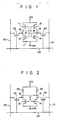
- Fig. 1 is a circuit diagram showing the configuration of a memory cell in a conventional CMOS static RAM memory as one of the above-mentioned RAMs.
- the memory cell has data storage flip-flop circuit 17 and transfer gate n-channel MOS transistors 23 and 24.
- input terminals of CMOS inverter 15, consisting of p-channel MOS transistor 11 and n-channel MOS transistor 13, and CMOS inverter 16, consisting of p-channel MOS transistor 12 and n-channel MOS transistor 14, are connected to each other's respective output terminals.
- the source-drain path of transistor 23 is inserted between data storage node 18 of circuit 17 and bit line 20.
- the gate of transistor 23 is connected to word line 22.
- the source-drain path of transistor 24 is inserted between data storage node 19 of circuit 17 and bit line 21.
- the gate of transistor 24 is connected to word line 22.
- Transistors 11 to 14, 23, and 24 are of enhancement type.
- Fig. 2 is a circuit diagram showing the configuration of an E/R type static RAM memory cell consisting of high impedance resistors and enhancement type MOS transistors.
- high impedance load resistors 25 and 26 are used in place of transistors 11 and 12 of circuit 17 in CMOS static RAM memory cell in Fig. 1.
- the CMOS static RAM cell is superior to the E/R type static RAM cell.
- power consumption of the CMOS static RAM cell is determined only by the leakage current of the respective transistors.
- the leakage current of transistors 13 and 14 as operating transistors in the E/R type static RAM cell must be supplied by resistors 25 and 26 as high impedance elements.
- resistors 25 and 26 In order to statically hold the data, a current which is about 100 times the leakage current of transistors 13 and 14 must be supplied to node 18 or 19. Since resistors 25 and 26 are normally made of polycrystalline silicon, it is difficult to maintain a low current level of resistors 25 and 26 when element micropatterning advances.
- Operational stability i.e., a power source margin, a noise margin, and resistance to soft error caused by alpha-rays
- the load elements are transistors (active elements) 11 and 12, and data storage nodes 18 and 19 can easily restore a high voltage level.
- the size of the CMOS static RAM cell is larger than that of the E/R type static RAM cell. Since the cell size determines the chip size, a small cell size provides advantages in integration and manufacturing cost.
- the cell consists of four MOS transistors and two resistors, as shown in Fig. 2.
- the resistors can be easily formed above the active elements (to be described later). For this reason, the cell size can be decreased and thus the packing density can be increased.
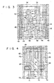
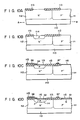
- the CMOS static RAM cell shown in Fig. 3 consists of six MOS transistors and an isolating region, required to isolate a p-type element from an n-type element.
- the size of the CMOS static RAM cell is larger than the E/R type static RAM cell.
- Fig. 3 is a plan view of the CMOS static RAM cell.
- reference numeral 31 denotes n-type diffusion regions constituting source and drain regions of n-channel transistors 13 and 14 (Fig. 1); and 32, p-type diffusion regions constituting source and drain regions of p-channel transistors 11 and 12 (Fig. 1).
- Reference numeral 33 denotes a first polycrystalline silicon layer serving as word line 22 of Fig. 1.
- Transfer gate transistors 23 and 24 are formed at intersection portions 34 and 35 between layer 33 and regions 31.
- Reference numerals 36 and 37 denote first polycrystalline silicon layers.
- Transistor 13, as part of CMOS inverter 15, is formed at intersection portion 38 between layer 36 and region 31, and transistor 14, as part of CMOS inverter 16, is formed at intersection portion 39 between layer 37 and region 31.
- transistor 11, as part of inverter 15, is formed at intersection portion 40 between layer 36 and region 32, and transistor 12, as part of inverter 16, is formed at intersection portion 41 between layer 37 and region 32.
- a right descending hatched line portion in Fig. 3 is second n-type polycrystalline silicon layer 42 connected to ground potential Vss and is connected to region 31 through contact hole 43.
- Left descending hatched line portions are aluminum wiring region 44 to 47.
- Layer 44 is one bit line which is connected to region 31 through contact hole 48.
- Layer 45 is the other bit line connected to region 31 through contact hole 49.
- Layer 46 is used as an interconnection layer for connecting regions 31 and 32 through contact holes 50 and 51, and to layer 37 as a gate wiring of p-channel MOS transistor 12 through contact hole 52.
- Layer 47 is used as an interconnection layer for connecting regions 31 and 32 through contact holes 53 and 54 and to layer 36 as the gate wiring of p-channel MOS transistor 11 through contact hole 54.
- Fig. 4 is a plan view showing a pattern of an E/R type static RAM cell.
- Reference numeral 61 denotes n-type diffusion regions serving as source and drain regions of n-channel MOS transistors 13, 14, 23, and 24 (Fig. 2).
- Reference numeral 62 denotes a first polycrystalline silicon layer serving as word line 22 of Fig. 2.
- Transfer gate transistors 23 and 24 (Fig. 2) are respectively formed at intersection portions 63 and 64 between layer 62 and region 61.
- Reference numerals 65 and 66 also denote first polycrystalline silicon layers.
- Drive transistors 13 and 14 in Fig. 2 are respectively formed at intersection portions 67 and 68 between layers 65 and 66 and region 61.
- a right descending hatched line portion in Fig. 4 is second polycrystalline silicon layer 69 connected to power source voltage Vcc, and part thereof constitutes resistors 25 and 26 in Fig. 2.
- Left descending hatched line portions are aluminum wiring layers 70, 71, and 72.
- Layers 71 and 72 constitute a pair of bit lines, as in Fig. 2.
- Layer 70 is connected to ground potential Vss and to region 61 through contact hole 73.
- a cell size of the static RAM cells will be described when the cells are integrated.
- a power source Vss line is constituted by second polycrystalline silicon layer 42.
- a wiring density of aluminum wiring layers 44 to 47 is four per cell.
- a second polycrystalline silicon layer density is one per cell.
- the two bit lines are constituted by aluminum wiring layers, and the high impedance resistor layers are constituted by the second polycrystalline silicon layer regions which are formed above the active elements.
- CMOS static RAM cell in Fig. 3 When the area of the CMOS static RAM cell in Fig. 3 is compared with that of the E/R static RAM cell in Fig. 4, its cell area is about 141% that of the cell in Fig. 4.
- the reason for the increase in cell size in Fig. 3 is the use of aluminum wiring layers. As is apparent from Figs. 3 and 4, four aluminum wiring layers are used in the cell in Fig. 3, while three aluminum wiring layers are used in the cell in Fig. 4.
- the width of the CMOS static RAM cell is determined by the number of aluminum wiring layers in the cell. Thus, it is very effective and desirable to decrease the number of aluminum wiring layers for reduction in cell size.
- E/R type static RAM cell it is very important to obtain a predetermined length to polycrystalline silicon layers.
- a decrease in the cell size in the longitudinal direction, that is, the direction of the length of the aluminum wiring layers is limited.
- the CMOS static RAM cell is superior to the E/R type static RAM cell when various characteristics are taken into consideration, but has limitations in cell size reduction.
- the E/R type static RAM cell generally has poorer electrical characteristics and limitations in cell size reduction.
- a multi-level interconnection system for integrated circuits comprising a first semiconductor region of a first conductivity type, a second semiconductor region of a second conductivity type and an interconnection layer containing an impurity of a second conductivity type, wherein said first semiconductor region forms a part of a p-n junction diode.
- the p-n junction diode is formed between said first semiconductor region being highly doped and a polycrystalline silicon wiring 211. Said p-n junction diode has a characteristic which is not satisfactory in cases where for example a diode is required for performing pull-up functions.
- - said interconnection layer connects said first semiconductor region with said second semiconductor region, said first semiconductor region being a drain region of a MOS transistor and said second semiconductor region being a gate electrode of said MOS transistor; - a third semiconductor region of said second conductivity type is provided which is formed in said first semiconductor region upon diffusion of the impurity from said interconnection layer to said first semiconductor region having the same crystalline semiconductor material as said third semiconductor region, and - said third semiconductor region is adapted to form, together with said first semiconductor region said p-n junction diode.
- the first semiconductor region of the first conductivity type and the second semiconductor region of the second conductivity type are connected by the interconnection layer which is made of a conductive material containing an impurity of the second conductivity type, in particular, a polycrystalline silicon.
- the number of aluminum interconnection layers in the memory cell of the present invention can be decreased as compared with that of the conventional memory cell. Therefore, the cell size can be decreased while good electrical characteristics are maintained.
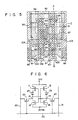
- Fig. 5 is a plan view showing a pattern of one memory cell.
- the cell is an integrated CMOS cell with elements like those in Fig. 1.
- reference numeral 81 denotes n-type diffusion regions, serving as source and drain regions of n-channel transistors 13, 14, 23, and 24.
- Reference numeral 82 denotes p-type diffusion regions serving as source and drain regions of p-channel transistors 11 and 12.
- Reference numeral 83 denotes a first polycrystalline silicon layer serving as word line 22.
- Transfer gate transistors 23 and 24 are respectively formed at intersection portions 84 and 85 between layer 83 and regions 81.
- Reference numerals 86 and 87 also denote first polysilicon layers, respectively.
- N-channel MOS transistors 13 and 14 constituting CMOS inverters 15 and 16 are formed at intersection portions 88 and 89 between regions 81 and layers 86 and 87.
- P-channel MOS transistors 11 and 12 constituting CMOS inverters 15 and 16 are respectively formed at intersection portions 90 and 91 between regions 82 and layers 86 and 87.
- Right descending hatched line portions are second polycrystalline silicon layers 92 and 93, containing an n-type impurity.
- Layer 92 is connected to regions 81 and 82 through contact holes 94 and 95, respectively, and to layer 87 through contact hole 96.
- Layer 93 is connected to region 81 through contact hole 97 and to parts of layer 86 and region 82 through contact hole 98.
- Left descending hatched line portions are aluminum wiring layers 99 to 101.
- Layer 100 is connected to one bit line and to part of region 81 through contact hole 102.
- Layer 101 is connected to the other bit line and to part of region 81 through contact hole 103.
- Layer 99 is connected to ground potential Vss, and is connected to region 81 through contact hole 104.
- the drains of the p- and n-channel MOS transistors constituting inverters 15 and 16 are connected not by the aluminum wiring layers but by second polycrystalline silicon layers 92 and 93 containing the n-type impurity.
- the Vss wiring layer is substituted from the conventional second polycrystalline silicon layer to aluminum wiring layer 99.
- three aluminum wiring layers and two second polycrystalline silicon layers are used, and the numbers of wiring layers of different materials are close, thus the cell size can be decreased as compared with the conventional CMOS arrangement in Fig. 3.
- the decrease in aluminum wiring layers is from four layers to three, thus the cell size can be decreased to be about 88% that of the conventional memory cell.
- the drains of the p-channel MOS transistors are constituted by regions 82, which are then connected to regions 81 as the drains of the n-channel MOS transistors through layer 92. For this reason, p-n junction diodes are formed between regions 82 and layer 92.
- p-n junction diodes 27 and 28 are respectively formed between the drains of transistors 11 and 13 and the drains of transistors 12 and 14 as the polarities of the diodes are shown therein.
- CMOS static RAM cell having diodes 27 and 28 between p- and n-channel MOS transistors will be described hereinafter.
- a DC high voltage level in the stable conditions at nodes 18 and 19 is increased to a level which satisfies I F > I, where I is the leakage current at nodes 18 and 19.
- the leakage current at nodes 18 and 19 is a sum of the leakage current in n-type diffusion regions 81 and an off current of n-channel MOS transistors 13 and 14, and is given as about 10 ⁇ 14 A/cell.
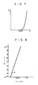
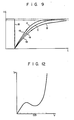
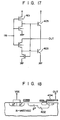
- Fig. 9 is a graph showing qualitative rising characteristics at node 19 when a signal of an illustrated waveform is supplied to node 18.
- Curve A shows rising characteristics at node 19 in the conventional CMOS static RAM cell in Fig. 1.
- Curve B shows rising characteristics at node 19 in the CMOS static RAM cell in Example 1.
- Curve A is determined by resistance characteristics of the p-channel MOS transistor.
- Curve B is determined by resistance characteristics of the p-channel MOS transistor and forward biasing characteristics of the diode.
- the rising characteristics at node 19 in Example 1 are slightly degraded as compared with those of the conventional RAM cell.
- the rising characteristics in Example 1 are sufficiently good as compared with those in the conventional E/R type static RAM cell. Therefore, data storage nodes can be sufficiently stable.
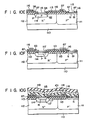
- FIGs. 10A to 10G and Figs. 11A to 11G are sectional views for explaining the steps in this manufacturing process.
- Figs. 10A to 10G are sectional views of the cell in Fig. 5, taken along the line A - B
- Figs. 11A to 11G are sectional views thereof taken along the line C - D.
- the same reference numerals in Figs. 10A to 11G denote the same parts as in Fig. 5. As shown in Figs.
- p- or n-type semiconductor substrate 110 is prepared as a support substrate, with p ⁇ -type semiconductor region 111 as a prospective region for source and drain of an n-channel MOS transistor, and n ⁇ -type semiconductor region 112 as a prospective region for source and drain of a p-channel MOS transistor, formed thereon. Subsequently, a surface portion of substate 1 which excludes the prospective source, drain, and channel regions of MOS transistors is selectively oxidized to form field insulating film 113.
- p-type impurity ions are implanted in a region surrounding a prospective p-n junction diode region.
- the doped ions are diffused by annealing, and p-type region 114 is formed.
- gate oxidation is performed to form gate oxide film 115, and a first polycrystalline silicon layer is deposited thereon.
- the first polycrystalline silicon layer is patterned to form polycrystalline silicon layers 83, 86, and 87, serving as gate electrodes of the MOS transistors.
- p- or n-type impurity ions are selectively implanted in the prospective source and drain regions of the p- and n-channel MOS transistors to form regions 81 and 82.
- silicon oxide film 116 is formed by, for example, CVD (Chemical Vapor Deposition) to cover the entire surface of the structure. Film 116 is then selectively etched to form contact holes 97 and 98.
- CVD Chemical Vapor Deposition
- film 115 on the surface of region 114 is selectively etched.
- a second polycrystalline silicon layer is then deposited to cover the entire surface.
- An n-type impurity is doped by ion implantation or phosphorus diffusion in this polycrystalline silicon layer.
- the doped silicon layer is then selectively patterned to form second polycrystalline silicon layers 92 and 93.
- the n-type impurity contained in layer 93 is diffused in region 114 to form n-type diffusion region 117.
- insulating interlayer 118 is formed by, for example, CVD, and is etched to form contact holes.
- Aluminum is then deposited to cover the entire surface and is patterned to form aluminum wiring layer 101.
- Protective film 119 is then formed on the entire surface to prepare the RAM cell of Example 1.
- Example 1 the n-type impurity is diffused from layer 92 for connecting region 82 to region 81, constituting the drain region of the n-channel MOS transistor to region 82, constituting the drain region of the p-channel MOS transistor, thereby forming the p-n junction diode.
- impurity concentrations of p- and n-type diffusion regions constituting the p-n junction diode are set to be higher than 1019 cm ⁇ 3.
- the p-n junction diode serves as an Esaki diode, the forward biasing characteristics of which provide a tunnel effect.
- the Esaki diode Since the Esaki diode has forward biasing characteristics as shown in Fig. 12, and a large current flows through the diode in a low voltage region. Therefore, low-voltage characteritics of the RAM cell can be improved as compared with the normal p-n junction diode. A resistance at the low voltage region is decreased. For this reason, a high voltage level at nodes 18 and 19 can be increased to the power source voltage Vcc, in the same manner as in the conventional CMOS static RAM cell, and thus a threshold voltage of the p-channel MOS transistor can be set to be a normal value.
- the AC rising characteristics of the Esaki diode are improved as compared with the RAM cell with a normal p-n junction diode (curve B), as indicated by curve C in Fig. 9. Attention need not be paid to the negative resistance or bottom current characteristics of the Esaki diode.
- the CMOS static RAM cell in Example 2 can be manufactured by the same process as that in Example 1, except that the impurity concentrations of regions 117 and 114 are controlled to be higher than 1019 cm ⁇ 3.
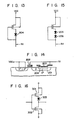
- Example 3 exemplifies a pull-up element which adapts the present invention.
- drain 201 and gate 202 of a PMOS are connected by interconnection layer 203 containing an n-type impurity.
- the impurity is diffused from the interconnection layer to drain 201, forming a p-n junction diode 204 therein.
- a potential at node N1 can be decreased by a voltage drop effected by a diode, as compared with a structure without a diode.
- the pull-up element may have series-connected diodes 205 and 206.
- Example 4 exemplifies a CMOS inverter.
- the drains of p- and n-channel MOS transistors 301 and 302 constituting the CMOS inverter are connected by a polycrystalline silicon interconnection layer containing an n-type impurity.
- the impurity is doped from the interconnection layer to the drain of transistor 301 to form p-n junction diode 303.
- Example 5 exemplifies a bipolar-CMOS inverter which adapts the present invention.
- drain 402 of p-channel MOS transistor 401 and the collector of bipolar transistor 403 are connected by interconnection layer 404 of polycrystalline silicon containing an n-type impurity.
- the impurity is doped from layer 404 to drain 402 to form a p-n junction diode.
- the p-n junction diode serves as an emitter-base junction of transistor 405.
- the bipolar-CMOS inverter requires a larger number of elements as compared with the CMOS inverter. However, as shown in Figs. 17 and 18, the present invention can simplify the pattern layout of the bipolar-CMOS inverter and decrease the base capacity thereof, thus guaranteeing high-speed operation of the device.
Landscapes
- Semiconductor Memories (AREA)
- Metal-Oxide And Bipolar Metal-Oxide Semiconductor Integrated Circuits (AREA)
- Electrodes Of Semiconductors (AREA)
- Bipolar Transistors (AREA)
Applications Claiming Priority (4)
| Application Number | Priority Date | Filing Date | Title |
|---|---|---|---|
| JP16140/85 | 1985-01-30 | ||
| JP60016140A JPS61174762A (ja) | 1985-01-30 | 1985-01-30 | 半導体装置およびその製造方法 |
| JP60016139A JPS61174761A (ja) | 1985-01-30 | 1985-01-30 | 半導体装置およびその製造方法 |
| JP16139/85 | 1985-01-30 |
Related Parent Applications (2)
| Application Number | Title | Priority Date | Filing Date |
|---|---|---|---|
| EP86101172.4 Division | 1986-01-29 | ||
| EP86101172A Division EP0192093B1 (fr) | 1985-01-30 | 1986-01-29 | Dispositif semi-conducteur et procédé pour sa fabrication |
Publications (2)
| Publication Number | Publication Date |
|---|---|
| EP0349022A2 true EP0349022A2 (fr) | 1990-01-03 |
| EP0349022A3 EP0349022A3 (fr) | 1991-07-24 |
Family
ID=26352396
Family Applications (3)
| Application Number | Title | Priority Date | Filing Date |
|---|---|---|---|
| EP19890116770 Withdrawn EP0349022A3 (fr) | 1985-01-30 | 1986-01-29 | Dispositif semi-conducteur |
| EP86101172A Expired - Lifetime EP0192093B1 (fr) | 1985-01-30 | 1986-01-29 | Dispositif semi-conducteur et procédé pour sa fabrication |
| EP89116769A Expired - Lifetime EP0349021B1 (fr) | 1985-01-30 | 1986-01-29 | Dispositif semi-conducteur et procédé pour sa fabrication |
Family Applications After (2)
| Application Number | Title | Priority Date | Filing Date |
|---|---|---|---|
| EP86101172A Expired - Lifetime EP0192093B1 (fr) | 1985-01-30 | 1986-01-29 | Dispositif semi-conducteur et procédé pour sa fabrication |
| EP89116769A Expired - Lifetime EP0349021B1 (fr) | 1985-01-30 | 1986-01-29 | Dispositif semi-conducteur et procédé pour sa fabrication |
Country Status (3)
| Country | Link |
|---|---|
| US (1) | US4907059A (fr) |
| EP (3) | EP0349022A3 (fr) |
| DE (2) | DE3672030D1 (fr) |
Cited By (1)
| Publication number | Priority date | Publication date | Assignee | Title |
|---|---|---|---|---|
| EP0585059A3 (fr) * | 1992-08-21 | 1995-07-19 | Sgs Thomson Microelectronics | Procédé de fabrication d'une cellule de mémoire du type vertical et structure obtenue par ce procédé. |
Families Citing this family (12)
| Publication number | Priority date | Publication date | Assignee | Title |
|---|---|---|---|---|
| JPH02101747A (ja) * | 1988-10-11 | 1990-04-13 | Toshiba Corp | 半導体集積回路とその製造方法 |
| JP2632420B2 (ja) * | 1989-02-23 | 1997-07-23 | 三菱電機株式会社 | 半導体集積回路 |
| US4999518A (en) * | 1989-12-08 | 1991-03-12 | International Business Machines Corp. | MOS switching circuit having gate enhanced lateral bipolar transistor |
| US5324958A (en) * | 1991-02-19 | 1994-06-28 | Synaptics, Incorporated | Integrating imaging systgem having wide dynamic range with sample/hold circuits |
| US5260592A (en) * | 1991-02-19 | 1993-11-09 | Synaptics, Incorporated | Integrating photosensor and imaging system having wide dynamic range with varactors |
| US5097305A (en) * | 1991-02-19 | 1992-03-17 | Synaptics Corporation | Integrating photosensor and imaging system having wide dynamic range |
| GB2254487B (en) * | 1991-03-23 | 1995-06-21 | Sony Corp | Full CMOS type static random access memories |
| GB2263018B (en) * | 1991-03-23 | 1995-06-21 | Sony Corp | Static random access memories |
| US5101257A (en) * | 1991-07-01 | 1992-03-31 | Motorola, Inc. | Semiconductor device having merged bipolar and MOS transistors and process for making the same |
| JP2965783B2 (ja) * | 1991-07-17 | 1999-10-18 | 三菱電機株式会社 | 半導体装置およびその製造方法 |
| US5212399A (en) * | 1991-08-15 | 1993-05-18 | Micron Technology, Inc. | Low cost polysilicon active p-channel load |
| TW230266B (fr) * | 1993-01-26 | 1994-09-11 | American Telephone & Telegraph |
Family Cites Families (15)
| Publication number | Priority date | Publication date | Assignee | Title |
|---|---|---|---|---|
| DE2133258A1 (de) * | 1971-07-05 | 1973-01-25 | Licentia Gmbh | Feldeffekttransistor aus einem halbleiterkoerper |
| US3753807A (en) * | 1972-02-24 | 1973-08-21 | Bell Canada Northern Electric | Manufacture of bipolar semiconductor devices |
| GB1441928A (en) * | 1972-12-18 | 1976-07-07 | Rca Corp | Peak detector |
| US4013489A (en) * | 1976-02-10 | 1977-03-22 | Intel Corporation | Process for forming a low resistance interconnect in MOS N-channel silicon gate integrated circuit |
| US4333099A (en) * | 1978-02-27 | 1982-06-01 | Rca Corporation | Use of silicide to bridge unwanted polycrystalline silicon P-N junction |
| SE444484B (sv) * | 1979-02-26 | 1986-04-14 | Rca Corp | Integrerad kretsanordning innefattande bl a en minnescell med en forsta och en andra inverterare |
| JPS55134962A (en) * | 1979-04-09 | 1980-10-21 | Toshiba Corp | Semiconductor device |
| JPS56125867A (en) * | 1980-03-10 | 1981-10-02 | Nec Corp | Semiconductor device |
| GB2098799B (en) * | 1981-05-20 | 1985-08-21 | Nippon Electric Co | Multi-level interconnection system for integrated circuits |
| EP0067661A1 (fr) * | 1981-06-15 | 1982-12-22 | Kabushiki Kaisha Toshiba | Dispositif à semi-conducteur et son procédé de fabrication |
| JPS5816564A (ja) * | 1981-07-09 | 1983-01-31 | インテル・コ−ポレ−シヨン | 相補形金属−酸化膜−半導体スタテイツクメモリセル |
| US4613886A (en) * | 1981-07-09 | 1986-09-23 | Intel Corporation | CMOS static memory cell |
| JPH0783252B2 (ja) * | 1982-07-12 | 1995-09-06 | 株式会社日立製作所 | 半導体集積回路装置 |
| US4487458A (en) * | 1982-09-28 | 1984-12-11 | Eaton Corporation | Bidirectional source to source stacked FET gating circuit |
| JPS59188959A (ja) * | 1983-04-11 | 1984-10-26 | Hitachi Ltd | 半導体集積回路装置及びマイクロコンピュータ |
-
1986
- 1986-01-29 EP EP19890116770 patent/EP0349022A3/fr not_active Withdrawn
- 1986-01-29 EP EP86101172A patent/EP0192093B1/fr not_active Expired - Lifetime
- 1986-01-29 DE DE8686101172T patent/DE3672030D1/de not_active Expired - Lifetime
- 1986-01-29 DE DE3650186T patent/DE3650186T2/de not_active Expired - Lifetime
- 1986-01-29 EP EP89116769A patent/EP0349021B1/fr not_active Expired - Lifetime
-
1988
- 1988-02-05 US US07/154,528 patent/US4907059A/en not_active Expired - Lifetime
Cited By (2)
| Publication number | Priority date | Publication date | Assignee | Title |
|---|---|---|---|---|
| EP0585059A3 (fr) * | 1992-08-21 | 1995-07-19 | Sgs Thomson Microelectronics | Procédé de fabrication d'une cellule de mémoire du type vertical et structure obtenue par ce procédé. |
| US5521401A (en) * | 1992-08-21 | 1996-05-28 | Sgs-Thomson Microelectronics, Inc. | P-N junction in a vertical memory cell that creates a high resistance load |
Also Published As
| Publication number | Publication date |
|---|---|
| EP0349021B1 (fr) | 1994-12-28 |
| EP0192093A1 (fr) | 1986-08-27 |
| EP0349021A2 (fr) | 1990-01-03 |
| EP0192093B1 (fr) | 1990-06-13 |
| DE3650186T2 (de) | 1995-05-24 |
| DE3650186D1 (de) | 1995-02-09 |
| EP0349021A3 (fr) | 1991-07-24 |
| DE3672030D1 (de) | 1990-07-19 |
| EP0349022A3 (fr) | 1991-07-24 |
| US4907059A (en) | 1990-03-06 |
Similar Documents
| Publication | Publication Date | Title |
|---|---|---|
| US4890148A (en) | Semiconductor memory cell device with thick insulative layer | |
| EP0952614B1 (fr) | Dispositif à effet de champ avec un canal en silicium polycristallin | |
| US6756692B2 (en) | Semiconductor storage device having high soft-error immunity | |
| US5187114A (en) | Method of making SRAM cell and structure with polycrystalline P-channel load devices | |
| US4297721A (en) | Extremely low current load device for integrated circuit | |
| US4639758A (en) | Metal oxide semiconductor field-effect transistor with metal source making ohmic contact to channel-base region | |
| US6479905B1 (en) | Full CMOS SRAM cell | |
| US4907059A (en) | Semiconductor bipolar-CMOS inverter | |
| US4290185A (en) | Method of making an extremely low current load device for integrated circuit | |
| US4780751A (en) | Semiconductor integrated circuit device | |
| EP0078222B1 (fr) | Cellule de mémoire bipolaire à circuit intégré | |
| EP0054471B1 (fr) | Elément de résistance semiconducteur | |
| US4251876A (en) | Extremely low current load device for integrated circuit | |
| KR0183485B1 (ko) | 반도체 디바이스 및 그 제조 방법 | |
| JP3400894B2 (ja) | スタティック型半導体記憶装置 | |
| EP0459380B1 (fr) | Dispositif de mémoire statique à semi-conducteurs | |
| JP2550119B2 (ja) | 半導体記憶装置 | |
| EP0111307A2 (fr) | Circuit intégré semi-conducteur comportant une résistance enterrée | |
| JPH06188389A (ja) | 集積回路2進メモリセル | |
| US5027186A (en) | Semiconductor device | |
| JP2515033B2 (ja) | 半導体スタティックメモリ装置の製造方法 | |
| JP2929438B2 (ja) | 半導体メモリ装置及びその製造方法 | |
| EP0517408A1 (fr) | Cellule et structure Sram avec des dispositifs de charge polycristallins à canal p | |
| JP2743672B2 (ja) | 半導体記憶装置 | |
| JPS61174762A (ja) | 半導体装置およびその製造方法 |
Legal Events
| Date | Code | Title | Description |
|---|---|---|---|
| PUAI | Public reference made under article 153(3) epc to a published international application that has entered the european phase |
Free format text: ORIGINAL CODE: 0009012 |
|
| 17P | Request for examination filed |
Effective date: 19890912 |
|
| AC | Divisional application: reference to earlier application |
Ref document number: 192093 Country of ref document: EP |
|
| AK | Designated contracting states |
Kind code of ref document: A2 Designated state(s): DE FR GB |
|
| PUAL | Search report despatched |
Free format text: ORIGINAL CODE: 0009013 |
|
| AK | Designated contracting states |
Kind code of ref document: A3 Designated state(s): DE FR GB |
|
| RHK1 | Main classification (correction) |
Ipc: H01L 27/11 |
|
| 17Q | First examination report despatched |
Effective date: 19921211 |
|
| APAB | Appeal dossier modified |
Free format text: ORIGINAL CODE: EPIDOS NOAPE |
|
| STAA | Information on the status of an ep patent application or granted ep patent |
Free format text: STATUS: THE APPLICATION IS DEEMED TO BE WITHDRAWN |
|
| 18D | Application deemed to be withdrawn |
Effective date: 19971021 |
|
| APAF | Appeal reference modified |
Free format text: ORIGINAL CODE: EPIDOSCREFNE |