EP0111307A2 - Circuit intégré semi-conducteur comportant une résistance enterrée - Google Patents
Circuit intégré semi-conducteur comportant une résistance enterrée Download PDFInfo
- Publication number
- EP0111307A2 EP0111307A2 EP83112313A EP83112313A EP0111307A2 EP 0111307 A2 EP0111307 A2 EP 0111307A2 EP 83112313 A EP83112313 A EP 83112313A EP 83112313 A EP83112313 A EP 83112313A EP 0111307 A2 EP0111307 A2 EP 0111307A2
- Authority
- EP
- European Patent Office
- Prior art keywords
- semiconductor
- resistor
- circuit
- substrate
- region
- Prior art date
- Legal status (The legal status is an assumption and is not a legal conclusion. Google has not performed a legal analysis and makes no representation as to the accuracy of the status listed.)
- Withdrawn
Links
- 239000004065 semiconductor Substances 0.000 title claims abstract description 40
- 239000000758 substrate Substances 0.000 claims abstract description 27
- 230000003068 static effect Effects 0.000 claims description 5
- 238000009792 diffusion process Methods 0.000 claims description 3
- 229910021420 polycrystalline silicon Inorganic materials 0.000 description 13
- 238000000034 method Methods 0.000 description 9
- 239000012535 impurity Substances 0.000 description 8
- VYPSYNLAJGMNEJ-UHFFFAOYSA-N Silicium dioxide Chemical compound O=[Si]=O VYPSYNLAJGMNEJ-UHFFFAOYSA-N 0.000 description 6
- 229910052681 coesite Inorganic materials 0.000 description 3
- 238000010276 construction Methods 0.000 description 3
- 229910052906 cristobalite Inorganic materials 0.000 description 3
- 230000000694 effects Effects 0.000 description 3
- 239000000377 silicon dioxide Substances 0.000 description 3
- 229910052682 stishovite Inorganic materials 0.000 description 3
- 229910052905 tridymite Inorganic materials 0.000 description 3
- 230000007547 defect Effects 0.000 description 2
- 238000005530 etching Methods 0.000 description 2
- 239000012212 insulator Substances 0.000 description 2
- 230000010354 integration Effects 0.000 description 2
- 239000002184 metal Substances 0.000 description 2
- 229910052581 Si3N4 Inorganic materials 0.000 description 1
- 238000010586 diagram Methods 0.000 description 1
- 238000002513 implantation Methods 0.000 description 1
- 238000005468 ion implantation Methods 0.000 description 1
- 238000002955 isolation Methods 0.000 description 1
- 239000000126 substance Substances 0.000 description 1
Images

Classifications
-
- H—ELECTRICITY
- H01—ELECTRIC ELEMENTS
- H01L—SEMICONDUCTOR DEVICES NOT COVERED BY CLASS H10
- H01L28/00—Passive two-terminal components without a potential-jump or surface barrier for integrated circuits; Details thereof; Multistep manufacturing processes therefor
- H01L28/20—Resistors
-
- H—ELECTRICITY
- H01—ELECTRIC ELEMENTS
- H01L—SEMICONDUCTOR DEVICES NOT COVERED BY CLASS H10
- H01L27/00—Devices consisting of a plurality of semiconductor or other solid-state components formed in or on a common substrate
- H01L27/02—Devices consisting of a plurality of semiconductor or other solid-state components formed in or on a common substrate including semiconductor components specially adapted for rectifying, oscillating, amplifying or switching and having potential barriers; including integrated passive circuit elements having potential barriers
- H01L27/04—Devices consisting of a plurality of semiconductor or other solid-state components formed in or on a common substrate including semiconductor components specially adapted for rectifying, oscillating, amplifying or switching and having potential barriers; including integrated passive circuit elements having potential barriers the substrate being a semiconductor body
- H01L27/10—Devices consisting of a plurality of semiconductor or other solid-state components formed in or on a common substrate including semiconductor components specially adapted for rectifying, oscillating, amplifying or switching and having potential barriers; including integrated passive circuit elements having potential barriers the substrate being a semiconductor body including a plurality of individual components in a repetitive configuration
-
- H—ELECTRICITY
- H01—ELECTRIC ELEMENTS
- H01L—SEMICONDUCTOR DEVICES NOT COVERED BY CLASS H10
- H01L27/00—Devices consisting of a plurality of semiconductor or other solid-state components formed in or on a common substrate
- H01L27/02—Devices consisting of a plurality of semiconductor or other solid-state components formed in or on a common substrate including semiconductor components specially adapted for rectifying, oscillating, amplifying or switching and having potential barriers; including integrated passive circuit elements having potential barriers
- H01L27/04—Devices consisting of a plurality of semiconductor or other solid-state components formed in or on a common substrate including semiconductor components specially adapted for rectifying, oscillating, amplifying or switching and having potential barriers; including integrated passive circuit elements having potential barriers the substrate being a semiconductor body
- H01L27/06—Devices consisting of a plurality of semiconductor or other solid-state components formed in or on a common substrate including semiconductor components specially adapted for rectifying, oscillating, amplifying or switching and having potential barriers; including integrated passive circuit elements having potential barriers the substrate being a semiconductor body including a plurality of individual components in a non-repetitive configuration
- H01L27/07—Devices consisting of a plurality of semiconductor or other solid-state components formed in or on a common substrate including semiconductor components specially adapted for rectifying, oscillating, amplifying or switching and having potential barriers; including integrated passive circuit elements having potential barriers the substrate being a semiconductor body including a plurality of individual components in a non-repetitive configuration the components having an active region in common
- H01L27/0705—Devices consisting of a plurality of semiconductor or other solid-state components formed in or on a common substrate including semiconductor components specially adapted for rectifying, oscillating, amplifying or switching and having potential barriers; including integrated passive circuit elements having potential barriers the substrate being a semiconductor body including a plurality of individual components in a non-repetitive configuration the components having an active region in common comprising components of the field effect type
- H01L27/0727—Devices consisting of a plurality of semiconductor or other solid-state components formed in or on a common substrate including semiconductor components specially adapted for rectifying, oscillating, amplifying or switching and having potential barriers; including integrated passive circuit elements having potential barriers the substrate being a semiconductor body including a plurality of individual components in a non-repetitive configuration the components having an active region in common comprising components of the field effect type in combination with diodes, or capacitors or resistors
- H01L27/0738—Devices consisting of a plurality of semiconductor or other solid-state components formed in or on a common substrate including semiconductor components specially adapted for rectifying, oscillating, amplifying or switching and having potential barriers; including integrated passive circuit elements having potential barriers the substrate being a semiconductor body including a plurality of individual components in a non-repetitive configuration the components having an active region in common comprising components of the field effect type in combination with diodes, or capacitors or resistors in combination with resistors only
-
- H—ELECTRICITY
- H10—SEMICONDUCTOR DEVICES; ELECTRIC SOLID-STATE DEVICES NOT OTHERWISE PROVIDED FOR
- H10B—ELECTRONIC MEMORY DEVICES
- H10B10/00—Static random access memory [SRAM] devices
- H10B10/15—Static random access memory [SRAM] devices comprising a resistor load element
Definitions
- the present invention relates to a semiconductor integrated circuit and, more particularly, to a semiconductor integrated circuit having a buried resistor.
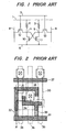
- FIG. 1 shows one example of the S-RAM.
- reference numeral 1 indicates a power supply line (at a potential Vcc); numerals 2 and 3 are load resistors; numerals 4 and 5 are load storage nodes; numeral 6 is a ground line (at a potential Vss); numeral 7 is a word line; numerals 8 and 9 are data lines; numerals-10 and 11 are MOS transistors (which will be shortly referred to as "MOSTs”) acting as driving transistors; and numerals 12 and 13 are transfer MOSTs.
- MOSTs MOS transistors
- the power supply line 1 is made of a highly doped polycrystalline silicon region identical to that forming the gates of the MOSTs 10 to 13, and the load resistors 2 and 3 are.formed by either leaving a portion of that polycrystalline silicon region as an intrinsic semiconductor region or making the same of a low doped region.
- the gate electrodes of the MOSTs 10 to 13, the power supply line 1 and the load resistors 2 and 3 are formed in a common plane.
- Fig. 2 shows one example of the plane pattern of the integrated circuit of Fig. 1.
- a region enclosed by single-dotted lines 30 provides the element region of a MOST, in which source and drain diffusion regions are formed across gates 31 and 37.
- reference numeral 31 indicates a power supply line; numerals 32 and 33 are load-resistors; numerals 34 and 35 are charge storage nodes; numeral 36 is a ground line; numeral 37 is a word line; and numerals 38 and 39 are data lines.
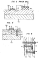
- a schematic section taken along line A - A' is shown in Fig. 3.
- a p-type well region 42 formed on a semiconductor substrate of n-type conductivity 41 is formed on its surface portion with a MOST which is composed of highly doped drain and source regions of n-type conductivity 43 and 44 and a polycrystalline silicon gate electrode 45.
- Reference numeral 46 in Fig. 3 indicates a gate insulating film.
- the resistors 32 and 33 are formed by either leaving a portion of the polycrystalline silicon identical to the gate electrode as an intrinsic semiconductor on a thick insulator 40 or lowly doping the same with an impurity.
- the drain region 43 is connected through-a load resistor 47 with the power supply line.
- the gate electrode of the MOST, the power supply line and the load resistor are formed in the common plane because of the pattern construction.
- the semiconductor integrated circuit of the prior art has a defect that it cannot effect sufficiently high integration.
- An object of the present invention is to provide a semiconductor device which can effect sufficiently high integration while eliminating the defect described in the above.
- the technique of forming the surface of a substrate with a deep hole having a small area is reported as a technique for forming a semiconductor element isolation region.
- the present invention contemplates a semiconductor integrated circuit by forming such a resistor of small area in the direction of deep of a semiconductor substrate as has its one end connected with a power supply.
- a well region of p-type conductivity 22 lying on a highly doped semiconductor substrate of n-type conductivity 21 made of Si or the like is formed in its surface portion with a MOST Q D which is composed of drain and source regions 23 and 24 of n-type conductivity and a gate electrode 25 of polycrystalline silicon.
- Reference numeral 26' in Fig. 4 indicates a gate insulating film.
- a resistor 27 which is made of a substance such as polycrystalline silicon and which is isolated from the p-type well ..”region 22 by an insulator 26 such as an oxide film.
- the gate electrode 25 and the upper portion 271 of the polycrystalline silicon acting as the resistor are made into the n-type regions by the impurities which are introduced while the drain and source regions are being formed, and the polycrystalline silicon region 272 located in the lower portion of the resistor is made into the n-type region by the impurities which will migrate up from the highly doped substrate so that either the ohmic contact with metal electrodes and so on.or the connection with the substrate can be made.
- the resistor 27 and the MOST Q D provide the elements corresponding to the elements 2 and 10 of Fig. 1 so that an inverter is constituted.
- the static memory cell shown in Fig. 1 can be made by additionally providing a pair of similar inverters to constitute a flip-flop circuit inbetween and by further providing an information transfer transistor.
- Fig. 5 shows one example of the plane pattern in which the example of Fig. 1 is constructed according to the present invention.
- Reference numerals 52 and 53 indicate resistor portions which are connected with the highly doped substrate at the power supply potential.
- the section taken along line B - B' of Fig. 5 is shown in Fig. 4.
- the effect that the memory cell can be highly integrated can be obtained according to the present invention from the facts that the load resistors formed on the semiconductor surface according to the prior art can be formed in the direction of the depth of the substrate and that it becomes unnecessary to provide the power supply line which is arranged on the substrate surface through the memory cells.
- the deep hole having the resistor 27 formed therein is formed in the drain region 23.
- hole may be formed either outside of the drain region 23 or in the boundary between the drain region 23 and the well 22.
- Figs. 6A to 6F are sectional views showing the consecutive steps of-the process for fabricating the semiconductor integrated circuit of the present invention.
- a p-type well region 62 (which has an impurity concentration of 10 16 cm -3 and a depth of 3 to 4 ⁇ m) is formed on an n-type highly doped Si substrate 61 (which has an impurity concentration of 1020 cm -3 ), and there is formed a hole which extends from the surface of said well to the substrate.
- a thin insulating film 66 (which is made of SiO 2 or Si 3 N 4 /SiO 2 having a thickness of 0.1 pm) is formed all over the surface. (Reference should be made to Fig. 6A.)
- the insulating film is selectively removed only from the bottom of the hole by the unisotropic etching technique or the like. (Reference should be made to Fig. 6B.)
- n-type impurity is then introduced into the drain and source regions of the MOST by the ion-implantation technique (with an implantation more than 10 13 cm -2 ). (Reference should be made to Fig. 6D.)
- drain and source regions 63 and 64 are formed by the thermal diffusion technique. (Reference should be made to Fig. 6E.)
- the polycrystalline silicon 67 buried in the hole has its upper region 671 and lower region 672 made into the n-type regions by the impurity implanted and by the impurity diffusing from the substrate, respectively.
- the description is made by taking up the n-channel type MOST as an example.
- the present invention can be realized even if a p-channel MOST is used by inverting the n- and p-types.
- the wells 22 and 62 may be semiconductor epitaxial growth regions of opposite type conductivity to that of the substrate, which is formed on the substrates 21 and 61.
- the construction of the semiconductor integrated circuit of the present invention is applied to the S-RAM. It is, however, quite natural that the present invention can be applied to another circuit.
Landscapes
- Engineering & Computer Science (AREA)
- Power Engineering (AREA)
- Computer Hardware Design (AREA)
- Microelectronics & Electronic Packaging (AREA)
- Physics & Mathematics (AREA)
- Condensed Matter Physics & Semiconductors (AREA)
- General Physics & Mathematics (AREA)
- Semiconductor Memories (AREA)
- Bipolar Integrated Circuits (AREA)
- Semiconductor Integrated Circuits (AREA)
Applications Claiming Priority (2)
| Application Number | Priority Date | Filing Date | Title |
|---|---|---|---|
| JP57216825A JPS59107563A (ja) | 1982-12-13 | 1982-12-13 | スタテイツク型半導体メモリ装置 |
| JP216825/82 | 1982-12-13 |
Publications (2)
| Publication Number | Publication Date |
|---|---|
| EP0111307A2 true EP0111307A2 (fr) | 1984-06-20 |
| EP0111307A3 EP0111307A3 (fr) | 1985-11-06 |
Family
ID=16694478
Family Applications (1)
| Application Number | Title | Priority Date | Filing Date |
|---|---|---|---|
| EP83112313A Withdrawn EP0111307A3 (fr) | 1982-12-13 | 1983-12-07 | Circuit intégré semi-conducteur comportant une résistance enterrée |
Country Status (3)
| Country | Link |
|---|---|
| EP (1) | EP0111307A3 (fr) |
| JP (1) | JPS59107563A (fr) |
| KR (1) | KR840007313A (fr) |
Cited By (5)
| Publication number | Priority date | Publication date | Assignee | Title |
|---|---|---|---|---|
| WO1989002655A1 (fr) * | 1987-09-14 | 1989-03-23 | Motorola, Inc. | Cellule de circuit integre a tranchee |
| EP0391123A2 (fr) * | 1989-04-04 | 1990-10-10 | Texas Instruments Incorporated | Résistance et capacité en tranchée et de longueur étendue |
| US8242068B2 (en) | 2008-12-05 | 2012-08-14 | Henkel Ag & Co. Kgaa | Cleaning agents |
| US8956938B2 (en) * | 2012-05-16 | 2015-02-17 | International Business Machines Corporation | Epitaxial semiconductor resistor with semiconductor structures on same substrate |
| CN111370474A (zh) * | 2020-04-23 | 2020-07-03 | 上海华虹宏力半导体制造有限公司 | 沟槽栅器件的栅极串联电阻 |
Citations (2)
| Publication number | Priority date | Publication date | Assignee | Title |
|---|---|---|---|---|
| FR2154553A1 (fr) * | 1971-09-27 | 1973-05-11 | Siemens Ag | |
| DE2947311A1 (de) * | 1978-11-24 | 1980-05-29 | Hitachi Ltd | Integrierte halbleiterschaltung |
-
1982
- 1982-12-13 JP JP57216825A patent/JPS59107563A/ja active Pending
-
1983
- 1983-12-07 EP EP83112313A patent/EP0111307A3/fr not_active Withdrawn
- 1983-12-12 KR KR1019830005883A patent/KR840007313A/ko not_active Application Discontinuation
Patent Citations (2)
| Publication number | Priority date | Publication date | Assignee | Title |
|---|---|---|---|---|
| FR2154553A1 (fr) * | 1971-09-27 | 1973-05-11 | Siemens Ag | |
| DE2947311A1 (de) * | 1978-11-24 | 1980-05-29 | Hitachi Ltd | Integrierte halbleiterschaltung |
Non-Patent Citations (1)
| Title |
|---|
| IBM TECHNICAL DISCLOSURE BULLETIN, vol. 24, no. 7A, December 1981, pages 3409-3412, New York, US; S.G. BARBEE et al.: "All ion-implant bipolar transistor process" * |
Cited By (8)
| Publication number | Priority date | Publication date | Assignee | Title |
|---|---|---|---|---|
| WO1989002655A1 (fr) * | 1987-09-14 | 1989-03-23 | Motorola, Inc. | Cellule de circuit integre a tranchee |
| EP0391123A2 (fr) * | 1989-04-04 | 1990-10-10 | Texas Instruments Incorporated | Résistance et capacité en tranchée et de longueur étendue |
| EP0391123A3 (fr) * | 1989-04-04 | 1991-09-11 | Texas Instruments Incorporated | Résistance et capacité en tranchée et de longueur étendue |
| US8242068B2 (en) | 2008-12-05 | 2012-08-14 | Henkel Ag & Co. Kgaa | Cleaning agents |
| US8956938B2 (en) * | 2012-05-16 | 2015-02-17 | International Business Machines Corporation | Epitaxial semiconductor resistor with semiconductor structures on same substrate |
| US9373637B2 (en) | 2012-05-16 | 2016-06-21 | Globalfoundries Inc. | Epitaxial semiconductor resistor with semiconductor structures on same substrate |
| CN111370474A (zh) * | 2020-04-23 | 2020-07-03 | 上海华虹宏力半导体制造有限公司 | 沟槽栅器件的栅极串联电阻 |
| CN111370474B (zh) * | 2020-04-23 | 2023-10-24 | 上海华虹宏力半导体制造有限公司 | 沟槽栅器件的栅极串联电阻 |
Also Published As
| Publication number | Publication date |
|---|---|
| JPS59107563A (ja) | 1984-06-21 |
| EP0111307A3 (fr) | 1985-11-06 |
| KR840007313A (ko) | 1984-12-06 |
Similar Documents
| Publication | Publication Date | Title |
|---|---|---|
| US5998276A (en) | Methods of making a SRAM cell employing substantially vertically elongated pull-up resistors and methods of making resistor constructions | |
| JP3057661B2 (ja) | 半導体装置 | |
| US5266507A (en) | Method of fabricating an offset dual gate thin film field effect transistor | |
| US7075153B2 (en) | Grounded body SOI SRAM cell | |
| EP0175378A2 (fr) | Mémoire dynamique à accès aléatoire (DRAM) | |
| EP0145606B1 (fr) | Dispositif de mémoire semi-conducteur | |
| KR900000820B1 (ko) | 반도체 메모리 장치 | |
| US5135888A (en) | Field effect device with polycrystalline silicon channel | |
| US4246593A (en) | High density static memory cell with polysilicon resistors | |
| US6656803B2 (en) | Radiation hardened semiconductor memory | |
| KR940001122B1 (ko) | 반도체장치 및 그 제조방법 | |
| US4780751A (en) | Semiconductor integrated circuit device | |
| US6009010A (en) | Static semiconductor memory device having data lines in parallel with power supply lines | |
| EP0192093B1 (fr) | Dispositif semi-conducteur et procédé pour sa fabrication | |
| JPH0150114B2 (fr) | ||
| US5757694A (en) | Balanced resistance load type SRAM cell | |
| JPH11145468A (ja) | 半導体装置およびその製造方法 | |
| EP0111307A2 (fr) | Circuit intégré semi-conducteur comportant une résistance enterrée | |
| US5323045A (en) | Semiconductor SRAM with low resistance power line | |
| US5761113A (en) | Soft error suppressing resistance load type SRAM cell | |
| JP2802752B2 (ja) | 半導体デバイスの構造 | |
| JPH07302846A (ja) | 半導体メモリ装置 | |
| US4823179A (en) | Semiconductor memory device with flip-flop memory cells which include polycrystalline load resistors | |
| US6150228A (en) | Method of manufacturing an SRAM with increased resistance length | |
| KR940001895B1 (ko) | 스태틱형 랜덤액세스메모리 |
Legal Events
| Date | Code | Title | Description |
|---|---|---|---|
| PUAI | Public reference made under article 153(3) epc to a published international application that has entered the european phase |
Free format text: ORIGINAL CODE: 0009012 |
|
| AK | Designated contracting states |
Designated state(s): DE FR GB NL |
|
| 17P | Request for examination filed |
Effective date: 19840516 |
|
| PUAL | Search report despatched |
Free format text: ORIGINAL CODE: 0009013 |
|
| AK | Designated contracting states |
Designated state(s): DE FR GB NL |
|
| 17Q | First examination report despatched |
Effective date: 19871016 |
|
| STAA | Information on the status of an ep patent application or granted ep patent |
Free format text: STATUS: THE APPLICATION IS DEEMED TO BE WITHDRAWN |
|
| 18D | Application deemed to be withdrawn |
Effective date: 19880227 |
|
| RIN1 | Information on inventor provided before grant (corrected) |
Inventor name: YAMAMOTO, SYUUICHI Inventor name: HANAMURA, SHOJI Inventor name: MASUHARA, TOSHIAKI Inventor name: MINATO, OSAMU Inventor name: SASAKI, TOSHIO |