EP0348916A2 - Einem MOSFET äquivalente Halbleitervorrichtung zur Spannungssteuerung - Google Patents
Einem MOSFET äquivalente Halbleitervorrichtung zur Spannungssteuerung Download PDFInfo
- Publication number
- EP0348916A2 EP0348916A2 EP89111707A EP89111707A EP0348916A2 EP 0348916 A2 EP0348916 A2 EP 0348916A2 EP 89111707 A EP89111707 A EP 89111707A EP 89111707 A EP89111707 A EP 89111707A EP 0348916 A2 EP0348916 A2 EP 0348916A2
- Authority
- EP
- European Patent Office
- Prior art keywords
- gate electrode
- semiconductor device
- voltage
- schottky junction
- electrode
- Prior art date
- Legal status (The legal status is an assumption and is not a legal conclusion. Google has not performed a legal analysis and makes no representation as to the accuracy of the status listed.)
- Withdrawn
Links
Images


Classifications
-
- H—ELECTRICITY
- H10—SEMICONDUCTOR DEVICES; ELECTRIC SOLID-STATE DEVICES NOT OTHERWISE PROVIDED FOR
- H10D—INORGANIC ELECTRIC SEMICONDUCTOR DEVICES
- H10D30/00—Field-effect transistors [FET]
-
- H—ELECTRICITY
- H10—SEMICONDUCTOR DEVICES; ELECTRIC SOLID-STATE DEVICES NOT OTHERWISE PROVIDED FOR
- H10D—INORGANIC ELECTRIC SEMICONDUCTOR DEVICES
- H10D12/00—Bipolar devices controlled by the field effect, e.g. insulated-gate bipolar transistors [IGBT]
- H10D12/211—Gated diodes
-
- H—ELECTRICITY
- H10—SEMICONDUCTOR DEVICES; ELECTRIC SOLID-STATE DEVICES NOT OTHERWISE PROVIDED FOR
- H10D—INORGANIC ELECTRIC SEMICONDUCTOR DEVICES
- H10D30/00—Field-effect transistors [FET]
- H10D30/60—Insulated-gate field-effect transistors [IGFET]
- H10D30/63—Vertical IGFETs
-
- H—ELECTRICITY
- H10—SEMICONDUCTOR DEVICES; ELECTRIC SOLID-STATE DEVICES NOT OTHERWISE PROVIDED FOR
- H10D—INORGANIC ELECTRIC SEMICONDUCTOR DEVICES
- H10D64/00—Electrodes of devices having potential barriers
- H10D64/60—Electrodes characterised by their materials
- H10D64/64—Electrodes comprising a Schottky barrier to a semiconductor
- H10D64/647—Schottky drain or source electrodes for IGFETs
Definitions
- the present invention relates to a semiconductor device, and more particularly to a voltage drive semiconductor device equivalent to a MOSFET.
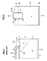
- a conventional vertical n-channel MOSFET as a voltage drive transistor, to be mainly used as a power device.
- the vertical n-channel MOSFET includes an n ⁇ -type drain region 1, a p-type channel region 2 formed therein, an n+-type source region 3 formed in the surface area of the channel region 2, a gate electrode 5 covered by a gate oxide film 4, formed on the drain and source regions 1 and 3 via the gate oxide film 4, a source electrode 6 formed on the channel and source regions 2 and 3, and a drain electrode 7 attached to the bottom of the drain region 1.
- the MOSFET of this kind usually, the source electrode 6 is connected to the ground, and a positive voltage is applied to the drain electrode 7.
- a MOSFET is a so-called voltage drive device which is driven by a variation of its gate voltage, and can be driven at a high speed and a low energy, in comparison with a bipolar transistor of a current-drive device. Accordingly, the MOSFET is widely used in a variety applications.
- the MOSFET has problems. Firstly, as shown in Fig. 1, the MOSFET includes an npn transistor composed of the drain, channel and source regions 1, 2 and 3 as a parasitic device. In the OFF condition that no voltage is applied to the gate electrode 5, when an avalanche breakdown takes place in the pn junction between the drain and channel regions 1 and 2, a hole current flows in the channel region 2 corresponding to the base of the parasitic transistor, and the parasitic transistor is actuated, resulting in a danger or fear of which the parasitic transistor is actuated and the current flowing in the device can not be correctly controlled.
- a semiconductor device comprising a semiconductor substrate having a first conductivity type, a metal electrode formed on the semiconductor substrate to form a Schottky junction therebetween, and a gate electrode arranged adjacent to the Schottky junction via an insulating film.
- FIG. 2 one embodiment of a semiconductor device according to the present invention.
- a source electrode 12 composed of a metallic material such as aluminum is formed on an n-type drain region 10 of a silicon semiconductor substrate having a first conductivity type to form a Schottky junction 20 therebetween.
- a gate electrode 14 is entirely covered by an insulating oxide film 16 and projects along therewith downwards into the upper portion of the drain region 10 and upwards outside across the source electrode 12.
- a drain electrode 18 is attached to the bottom of the drain region 10.
- the thickness of the insulating oxide film 16 it is preferably thinner for actuating a sufficient electric field to the silicon drain region 10, and, meanwhile, it is preferably thicker for obtaining a sufficient insulating resistant pressure between the source and gate electrodes 12 and 14. Accordingly, it is determined to a suitable thickness, e.g., 200 to 500 angstrom to properly satisfy these conditions.
- the source electrode 12 is connected to the ground, and a positive voltage V DS is applied to the drain electrode 18.
- the semiconductor device when the gate electrode 14 is connected to the ground, the semiconductor device has the same reverse bias characteristics as those of a usual Schottky diode. Hence, no current flows between the drain region 10 and source electrode 12 until the drain voltage V DS becomes a sufficiently high voltage V B .
- the drain voltage V DS becomes larger than the V B the tunnel phenomenon is caused, and a current is started to rapidly flow between the drain region 10 and source electrode 12.
- the impurity concentration of the silicon constituting the drain region 10 is relatively low, an avalanche breakdown is caused at a certain voltage before the tunnel phenomenon is caused, and a current is started to flow between the drain region 10 and source electrode 12.
- the drain voltage V DS is maintained to less than the relatively high voltage V B , and in this condition, by selectively applying a positive voltage to the gate electrode 14, the control of the current flowing between the drain region 10 and source electrode 12.
- a strong electric field is partially affected to a region S of the Schottky junction 20 adjacent to the gate electrode 14, as shown in Fig. 3, and an apparent thickness of a barrier layer composed of the Schottky junction 20 is reduced due to the electric field concentration.
- V DS is less than the certain voltage V B
- the tunnel phenomenon is caused, and the current is started to flow between the drain region 10 and source electrode 12.
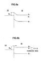
- a one-dotted line IV-IV indicates a linear area which extends parallel with the insulating oxide film 16 across the Schottky junction 20 and is slightly apart from the insulating oxide film 16.
- Figs. 4a and 4b show the energy bands of the linear area IV-IV in Fig. 2.
- the solid lines are obtained when the drain voltage V DS less than the certain voltage V B is applied in the device (V B ⁇ V DS ⁇ 0) and the gate electrode 14 is connected to the ground.
- the broken lines are obtained when a positive voltage is applied to the gate electrode 14.
- the drain voltage V DS is lower than the gate voltage V G , and an electron accumulation layer can be sometimes formed around the gate electrode 14.
- the thickness of the barrier layer of the Schottky junction 20 is reduced by the accumulated electrons, and the tunnel current is continuously flowed.
- the voltage of the accumulation layer around the gate electrode 14 becomes equal to the voltage of the source electrode 12, and, even when the voltage of the drain region 10 becomes lower than that of the gate electrode 14, the current keeps on flowing.
- Fig. 6a there is shown an energy band of the Schottky junction between the drain region of the n-type silicon and the source electrode 12 of the metal.
- ⁇ B there exists an energy barrier ⁇ B in the junction between these two members according to a difference between the work functions thereof.
- the metal side is forward-biased, as shown in Fig. 6b, the electronic current flows from the silicon side to the metal side.
- the metal side is reverse-biased, as shown in Fig. 6c, the electrons of the metal side can not clear the energy barrier ⁇ B , and the current hardly flows.
- a sufficiently large reverse-bias is given to the metal side, as shown in Fig.
- the thickness of the energy barrier is reduced, and the current flows due to the tunnel phenomenon.
- the condition for starting to flow the current in a macroscopic view is determined as follows. That is, for instance, the energy barrier in Fig. 6d, in other words, the thickness ⁇ of the Schottky barrier which is the distance from the position of the junction in the energy band figure to the intersection between the Fermi level and the lower end line of the conduction band inclined due to the electric field of the semiconductor, is determined to approximately 100 angstrom.
- the thickness of the energy barrier of the Schottky junction reverse-biased is modulated by the electric field of the gate electrode to control the tunnel phenomenon, thereby controlling the main current in the device.
- a vertical groove C is formed in the surface area of a drain region 10 composed of an n-type silicon semiconductor substrate, and the surface portion of the grooved drain region 10 is oxidized to for an insulating gate oxide film 16 if formed.
- a conductive polycrystalline silicon layer P is deposited over the surface of the drain region 10 to fill up the groove C with the polycrystalline silicon layer P.
- the polycrystalline silicon layer P is etched so that the polycrystalline silicon layer P remains only in the groove C, as shown in Fig. 7b.
- the polycrystalline silicon layer P in the groove C will constitute a gate electrode 14.
- Fig. 7c the surface of the polycrystalline silicon layer P in the groove C is oxidized. Since the oxidizing rate of the polycrystalline silicon is more quick than that of the monocrystalline silicon constituting the drain region 10, the surface of the object shown in Fig. 7b is oxidized and then the resulted oxide film is etched to form the structure where the oxide film is formed only on the polycrystalline silicon layer P and the n-type silicon is exposed outside beside the oxide film, as shown in Fig. 7c. Then, only the n-type silicon substrate for the drain region 10 is etched in a suitable depth to form the structure shown in Fig. 7d.
- a metallic material is deposited on the n-type silicon substrate to form a Schottky junction therebetween to form a semiconductor device according to the present invention, as shown in Fig. 2.
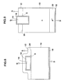
- FIGs. 8 and 9 there are shown other embodiments of a semiconductor device according to the present invention.
- a gate electrode 14 wholly covered by an insulating oxide film 16 is formed on the flat surface of a drain region 10 and as well as in a plane containing a Schottky junction 20 between the drain region 10 and a metallic source electrode 12.
- the metallic source electrode 12 entirely covers the gate electrode 14 covered by the insulating oxide film 16.
- the gate electrode 14 covered by the insulating oxide film 16 is not projected into the drain region 10, and hence the semiconductor device can be produced easier in a simpler method than the one shown in Figs. 2 and 7.
- the metallic source electrode 12 may be lowered with a depth of approximately the same thickness of the side wall of the insulating oxide film 16 covering the gate electrode 14 to form the Schottky junction 20 right under the insulating oxide film 16, with the result of effective characteristics.
- a p+-type anode region 22 is further interposed between an n-type silicon drain region 10 and a drain electrode 18 in comparison with the embodiment shown in Fig. 2.
- the hole injection from the p-type anode region 22 into the drain region 10 is carried out, and a semiconductor device having a further lower ON-resistance can be obtained in virtue of the conductivity modulation effect.
- a semiconductor device having a further lower ON-resistance can be obtained in virtue of the conductivity modulation effect.
- there is no parasitic thyristor which arises a problem in a conventional conductivity modulation type MOSFET (IGBT), and accordingly no latch-up phenomenon takes place.
Landscapes
- Electrodes Of Semiconductors (AREA)
- Metal-Oxide And Bipolar Metal-Oxide Semiconductor Integrated Circuits (AREA)
- Junction Field-Effect Transistors (AREA)
- Insulated Gate Type Field-Effect Transistor (AREA)
Applications Claiming Priority (2)
| Application Number | Priority Date | Filing Date | Title |
|---|---|---|---|
| JP158317/88 | 1988-06-27 | ||
| JP63158317A JPH027571A (ja) | 1988-06-27 | 1988-06-27 | 半導体装置 |
Publications (2)
| Publication Number | Publication Date |
|---|---|
| EP0348916A2 true EP0348916A2 (de) | 1990-01-03 |
| EP0348916A3 EP0348916A3 (de) | 1991-02-06 |
Family
ID=15668993
Family Applications (1)
| Application Number | Title | Priority Date | Filing Date |
|---|---|---|---|
| EP19890111707 Withdrawn EP0348916A3 (de) | 1988-06-27 | 1989-06-27 | Einem MOSFET äquivalente Halbleitervorrichtung zur Spannungssteuerung |
Country Status (2)
| Country | Link |
|---|---|
| EP (1) | EP0348916A3 (de) |
| JP (1) | JPH027571A (de) |
Cited By (7)
| Publication number | Priority date | Publication date | Assignee | Title |
|---|---|---|---|---|
| EP0469611A1 (de) * | 1990-08-03 | 1992-02-05 | Hitachi, Ltd. | Tunnelinjektions-Halbleiterbauelement und dessen Herstellungsverfahren |
| US6433396B1 (en) * | 1999-10-05 | 2002-08-13 | International Rectifier Corporation | Trench MOSFET with integrated schottky device and process for its manufacture |
| EP3255676A1 (de) * | 2016-06-09 | 2017-12-13 | ABB Schweiz AG | Vertikales leistungshalbleiterbauelement und verfahren zum betrieb solch eines bauelements |
| CN112599603A (zh) * | 2020-12-16 | 2021-04-02 | 西安电子科技大学 | 基于纵向肖特基源隧穿结的准垂直场效应晶体管及方法 |
| CN112614889A (zh) * | 2020-12-16 | 2021-04-06 | 西安电子科技大学 | 基于纵向肖特基源隧穿结的全垂直场效应晶体管及方法 |
| DE102016115218B4 (de) | 2015-08-21 | 2024-09-26 | Infineon Technologies Ag | Latch-Up-freier Leistungstransistor |
| US12501668B2 (en) | 2020-12-03 | 2025-12-16 | Hitachi Energy Ltd | Power semiconductor device and a method for producing a power semiconductor device |
Families Citing this family (5)
| Publication number | Priority date | Publication date | Assignee | Title |
|---|---|---|---|---|
| JP2002334997A (ja) * | 2001-05-08 | 2002-11-22 | Shindengen Electric Mfg Co Ltd | Mosトレンチを有するショットキー障壁整流装置及びその製造方法 |
| JP2011176026A (ja) * | 2010-02-23 | 2011-09-08 | Fuji Electric Co Ltd | 半導体素子の製造方法 |
| JP2011198938A (ja) * | 2010-03-18 | 2011-10-06 | Toshiba Corp | トランジスタ |
| KR20120120825A (ko) * | 2011-04-25 | 2012-11-02 | 삼성전기주식회사 | 질화물 반도체 소자 및 그 제조방법 |
| JP7510295B2 (ja) * | 2020-02-18 | 2024-07-03 | 株式会社東芝 | 半導体装置 |
Family Cites Families (2)
| Publication number | Priority date | Publication date | Assignee | Title |
|---|---|---|---|---|
| GB2111745B (en) * | 1981-12-07 | 1985-06-19 | Philips Electronic Associated | Insulated-gate field-effect transistors |
| US4485550A (en) * | 1982-07-23 | 1984-12-04 | At&T Bell Laboratories | Fabrication of schottky-barrier MOS FETs |
-
1988
- 1988-06-27 JP JP63158317A patent/JPH027571A/ja active Pending
-
1989
- 1989-06-27 EP EP19890111707 patent/EP0348916A3/de not_active Withdrawn
Cited By (7)
| Publication number | Priority date | Publication date | Assignee | Title |
|---|---|---|---|---|
| EP0469611A1 (de) * | 1990-08-03 | 1992-02-05 | Hitachi, Ltd. | Tunnelinjektions-Halbleiterbauelement und dessen Herstellungsverfahren |
| US6433396B1 (en) * | 1999-10-05 | 2002-08-13 | International Rectifier Corporation | Trench MOSFET with integrated schottky device and process for its manufacture |
| DE102016115218B4 (de) | 2015-08-21 | 2024-09-26 | Infineon Technologies Ag | Latch-Up-freier Leistungstransistor |
| EP3255676A1 (de) * | 2016-06-09 | 2017-12-13 | ABB Schweiz AG | Vertikales leistungshalbleiterbauelement und verfahren zum betrieb solch eines bauelements |
| US12501668B2 (en) | 2020-12-03 | 2025-12-16 | Hitachi Energy Ltd | Power semiconductor device and a method for producing a power semiconductor device |
| CN112599603A (zh) * | 2020-12-16 | 2021-04-02 | 西安电子科技大学 | 基于纵向肖特基源隧穿结的准垂直场效应晶体管及方法 |
| CN112614889A (zh) * | 2020-12-16 | 2021-04-06 | 西安电子科技大学 | 基于纵向肖特基源隧穿结的全垂直场效应晶体管及方法 |
Also Published As
| Publication number | Publication date |
|---|---|
| JPH027571A (ja) | 1990-01-11 |
| EP0348916A3 (de) | 1991-02-06 |
Similar Documents
| Publication | Publication Date | Title |
|---|---|---|
| US4689647A (en) | Conductivity modulated field effect switch with optimized anode emitter and anode base impurity concentrations | |
| US7232726B2 (en) | Trench-gate semiconductor device and method of manufacturing | |
| EP1271654B1 (de) | Halbleiterbauelement und verfahren zu seiner herstellung | |
| US5828100A (en) | Insulated gate semiconductor device having trench gate and inverter provided with the same | |
| US6762098B2 (en) | Trench DMOS transistor with embedded trench schottky rectifier | |
| US7795638B2 (en) | Semiconductor device with a U-shape drift region | |
| JP5790214B2 (ja) | 横型の絶縁ゲート型バイポーラトランジスタ | |
| US5289019A (en) | Insulated gate bipolar transistor | |
| US6091107A (en) | Semiconductor devices | |
| US6262470B1 (en) | Trench-type insulated gate bipolar transistor and method for making the same | |
| US4989058A (en) | Fast switching lateral insulated gate transistors | |
| EP0348916A2 (de) | Einem MOSFET äquivalente Halbleitervorrichtung zur Spannungssteuerung | |
| JPH09331062A (ja) | 半導体装置およびその製造方法 | |
| JP2633145B2 (ja) | 半導体横方向絶縁ゲートバイポーラトランジスタ装置 | |
| JP3255547B2 (ja) | 絶縁ゲート付きサイリスタ | |
| US4933740A (en) | Insulated gate transistor with vertical integral diode and method of fabrication | |
| US20020093049A1 (en) | Field effect-controllable semiconductor component with two-directional blocking, and a method of producing the semiconductor component | |
| JPH023980A (ja) | 縦型電界効果トランジスタ | |
| US4969024A (en) | Metal-oxide-semiconductor device | |
| EP0785582A2 (de) | MOS-gesteuerter Thyristor mit Grabengate | |
| KR100370957B1 (ko) | 트렌치구조의 폴리실리콘 영역을 구비하는 고전압소자 및그 제조방법 | |
| US5212396A (en) | Conductivity modulated field effect transistor with optimized anode emitter and anode base impurity concentrations | |
| CN100416858C (zh) | 半导体器件 | |
| JP2001284574A (ja) | 絶縁ゲート付き半導体装置 | |
| KR100218261B1 (ko) | 모스 제어형 사이리스터 및 그 제조방법 |
Legal Events
| Date | Code | Title | Description |
|---|---|---|---|
| PUAI | Public reference made under article 153(3) epc to a published international application that has entered the european phase |
Free format text: ORIGINAL CODE: 0009012 |
|
| 17P | Request for examination filed |
Effective date: 19890627 |
|
| AK | Designated contracting states |
Kind code of ref document: A2 Designated state(s): DE GB |
|
| PUAL | Search report despatched |
Free format text: ORIGINAL CODE: 0009013 |
|
| RHK1 | Main classification (correction) |
Ipc: H01L 29/56 |
|
| AK | Designated contracting states |
Kind code of ref document: A3 Designated state(s): DE GB |
|
| STAA | Information on the status of an ep patent application or granted ep patent |
Free format text: STATUS: THE APPLICATION IS DEEMED TO BE WITHDRAWN |
|
| 18D | Application deemed to be withdrawn |
Effective date: 19930105 |