EP0348815A2 - Verfahren und Vorrichtung, um auf dielektrische Filme montierte Halbleiterbandelemente einzukapseln - Google Patents
Verfahren und Vorrichtung, um auf dielektrische Filme montierte Halbleiterbandelemente einzukapseln Download PDFInfo
- Publication number
- EP0348815A2 EP0348815A2 EP89111334A EP89111334A EP0348815A2 EP 0348815 A2 EP0348815 A2 EP 0348815A2 EP 89111334 A EP89111334 A EP 89111334A EP 89111334 A EP89111334 A EP 89111334A EP 0348815 A2 EP0348815 A2 EP 0348815A2
- Authority
- EP
- European Patent Office
- Prior art keywords
- film
- coating
- components
- curing chamber
- curing
- Prior art date
- Legal status (The legal status is an assumption and is not a legal conclusion. Google has not performed a legal analysis and makes no representation as to the accuracy of the status listed.)
- Withdrawn
Links
Images

Classifications
-
- H—ELECTRICITY
- H10—SEMICONDUCTOR DEVICES; ELECTRIC SOLID-STATE DEVICES NOT OTHERWISE PROVIDED FOR
- H10P—GENERIC PROCESSES OR APPARATUS FOR THE MANUFACTURE OR TREATMENT OF DEVICES COVERED BY CLASS H10
- H10P72/00—Handling or holding of wafers, substrates or devices during manufacture or treatment thereof
- H10P72/04—Apparatus for manufacture or treatment
- H10P72/0448—Apparatus for applying a liquid, a resin, an ink or the like
-
- B—PERFORMING OPERATIONS; TRANSPORTING
- B05—SPRAYING OR ATOMISING IN GENERAL; APPLYING FLUENT MATERIALS TO SURFACES, IN GENERAL
- B05C—APPARATUS FOR APPLYING FLUENT MATERIALS TO SURFACES, IN GENERAL
- B05C9/00—Apparatus or plant for applying liquid or other fluent material to surfaces by means not covered by any preceding group, or in which the means of applying the liquid or other fluent material is not important
- B05C9/04—Apparatus or plant for applying liquid or other fluent material to surfaces by means not covered by any preceding group, or in which the means of applying the liquid or other fluent material is not important for applying liquid or other fluent material to opposite sides of the work
Definitions
- This invention relates generally to coating of articles, and more specifically, to the coating of semiconductor components which are secured within an aperture in a dielectric film.
- a further object of this invention is to provide apparatus for coating semiconductor components on a flexible film wherein the size of the apparatus for providing such coating is substantially reduced.
- Apparatus for applying a coating composition to semiconductor components such as silicon chips mounted in an aperture in a dielectric film.
- the film is passed from a storage reel beneath a spray applicator which applies the coating composition to the upperside of the chip.
- the film then passes into a curing chamber for curing and setting the composition.
- the film subsequently passes outwardly of the chamber and over a substantially square sprocket having standard prongs to mate with perforations in the film which reverses the direction of the film and leads it towards the curing chamber.
- a second apparatus Prior to entering the chamber, a second apparatus applies the coating composition on the other side of the chip.
- the film then returns to the curing chamber so that the second coating may be cured and set, and then passes over a further substantially square sprocket and is led outwardly from the curing chamber and stored on a reel.
- the sides of the substantially square sprocket are of a dimension such that the film bends only between the semiconductor components or a group of semiconductor components on the film.
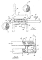
- a supply reel 11 which has wound thereon flexible film having semiconductor components such as silicone chips mounted above an aperture in the film and supported by input-output connectors connected to the interior edge of the aperture. Associated conductors are etched or printed on the film. There is a small spacing on the film between each of the components and their input-output connectors.
- semiconductor components such as silicone chips mounted above an aperture in the film and supported by input-output connectors connected to the interior edge of the aperture.
- Associated conductors are etched or printed on the film. There is a small spacing on the film between each of the components and their input-output connectors.
- supply reel 11 In order not to damage the components mounted on the film, supply reel 11 must have a substantial spindle diameter since any extreme bending of the components could damage them. Such a diameter is indicated by the interrupted lines.
- Film 13 is shown passing from supply reel 11 past applicator 21.
- This may be a standard type of micro-dot applicator which is used to apply the desired coating composition on the upper side of the chip mounted relative to film 13.
- the film then passes through curing chamber 14 so as to cure and set the coating composition applied to the chip by applicator 21, and passes outwardly of curing chamber 14 and over square sprocket 15 so as to reverse the direction of the film.
- the sides of the substantially square sprocket 15 are of a dimension such that the film is only bent traversely between each individual component or a series of components if the size warrants.
- a second applicator 27 applies the coating composition on the opposite side of the chip.
- the film then reenters the curing oven 14 so as to cure and set the second application of coating composition and passes about square sprocket 17 so as to reverse direction and lead it outwardly from the curing chamber 14.
- the film passes over two sides of sprocket 19 and is then wound on take-up reel 26.
- Take-up reel 26 is power-driven so as to supply the necessary movement of the film. In some cases it may be desirable to drive square sprockets 15, 17 and 19. If so, the rotation of these sprockets must be coordinated with the rotational speed of take-up reel 26.
- methods of curing may be used. All of the methods used are designed to accelerate the curing so that this may be a continuous operation from the supply reel to the take-up reel.
- Standard heaters 24 may be used to control the inside heat of the curing chamber 14. These may be electrical, gas, etc. If sufficient heat is provided by lamps, such lamps 25, mounted on frame 23, and lamps 31, mounted on frame 29, may also be used. These lamps may be ultraviolet lamps or infrared lamps for supplying the necessary heat.
- Fig. 2 is an enlarged schematic of a portion of the film of Fig. 1.
- Film 13 includes aperture 46 with chip 44 being supported above the aperture by a plurality of input-output connectors 15 which are secured to the inner periphery of aperture 32 by conductive bonding material 18 (Fig. 3).
- Leads 20 are etched or coated on film 13 so as to interconnect chip 44 with conductive strips 22. This construction is known in the art.
- the schematic illustration of Fig. 3 shows chip 44 after coating 28 has been cured in chamber 14 and coating 30 has just been applied by applicator 27 such as a micro-dot applicator. As can be seen, both major faces of chip 44 have been coated.
- compositions are radiation curable and, in such cases, ultraviolet lamps may be used. In still other possible curing applications an electron beam may be used.
- FIG. 1 there is shown air intake 33 and exhaust 37, with chamber 35 downstream of the air path from air intake 33.
- This chamber may be used for introducing carbon dioxide for accelerating and curing certain compositions and/or it may be used for introducing additional moisture to further accelerate curing of moisture-curable systems.
- Fig. 4 is a detailed perspective view of a substantially square sprocket such as sprocket 15.
- Sprocket 15 has standard teeth 12 which mate with perforations 39 on the edges of the film.
- Semiconductor components 41, 42, 43, 44, and 45 are shown as they are passing about sprocket 15, which rotates in the direction of the arrow.
- the length of the sides of the sprocket are coordinated with the spacing of the semiconductor components on the film so that bending of the film occurs only on a line between the components where there are no wires or parts of the components.
- the coating composition which may be used to coat the electrical chips may be curable silicone compositions, an epoxy resin, or a urethane composition.
- the curable silicone compositions consist of crosslinkable organopolysiloxanes or modified organopolysiloxanes, a crosslinking agent and a catalyst, if desired.
- the organopolysiloxanes employed in the curable coating composition may be a diorganopolysiloxane having the general formula R1(SiR2O) x SiR2R1 in which R represents the same or different monovalent hydrocarbon radicals having from 1 to 18 carbon atoms, R1 represents condensable groups, hydrolyzable groups, monovalent hydrocarbon radicals and monovalent hydrocarbon radicals having aliphatic unsaturation and x is a number greater than 10.
- organopolysiloxanes which may be employed are organopolysiloxanes having organic polymers which are linked by chemical bonding to organopolysiloxanes, including diorganopolysiloxanes, and which represent graft polymers or block copolymers or those formed in the presence of organopolysiloxanes by the polymerization of at least one organic compound having at least one aliphatic carbon-carbon double bond.
- a two-component room temperature vulcanizable organopolysiloxane composition may be employed in which hydroxyl-terminated diorganopolysiloxanes are crosslinked by the ad dition of polyalkoxysilanes of the formula (R3O) n SiR2 4-n or polyalkoxysiloxanes in which the silicon atoms are linked through ⁇ Si-O-Si ⁇ linkages and the remaining valences of the silicon atoms are satisfied by R2 and R3O radicals and catalysts.
- R2 is a monovalent hydrocarbon radical or a halogenated monovalent hydrocarbon radical having from 1 to 10 carbon atoms
- R3 is a monovalent hydrocarbon radical having from 1 to 10 carbon atoms
- n is 3 or 4.
- Heat-curable organopolysiloxanes which are crosslinked in the presence of peroxides may also be employed in this invention.
- an electron beam is employed as a heat source to produce curing.
- the organopolysiloxanes are preferably diorganopolysiloxanes having the following formula R1(SiR2O) x SiR2R1 where R and x are the same as above and R1 is a monovalent hydrocarbon carbon radical or a radical having aliphatic unsaturation.
- the diorganopolysiloxane When the organopolysiloxane compositions are crosslinked by the addition of Si-bonded hydrogen to an aliphatically unsaturated carbon-to-carbon group, the diorganopolysiloxane may be represented by the formula R1(SiR2O) x SiR2R1 where R and x are the same as above and R1 is an aliphatically unsaturated radical.
- Organohydrogenpolysiloxanes employed as crosslinking agents in the compositions of this invention generally consist of units of the general formula R4 m SiO (4-m)/2 where R4 represents hydrogen, a monovalent hydrocarbon radical or a halogenated monovalent hydrocarbon radical having from 1 to 18 carbon atoms, in which at least two and preferably three Si-bonded hydrogen atoms are present per molecule, and m is 1, 2 or 3.
- Platinum catalysts which are employed in these compositions, may consist of finely dispersed platinum as well as platinum compounds and/or platinum complexes which have been used heretofore to promote the addition of Si-bonded hydrogen atoms to compounds having aliphatically unsaturated groups.
- Radiation curable silicone compositions may be used in the present invention for coating electrical chips.
- Ultraviolet radiation is one of the most widely used types of radiation because of its low cost and shorter cure times.
- heat-sensitive materials can be safely coated and cured with ultraviolet radiation because of the relatively low temperatures involved.
- Radiation polymerizable compositions containing organopolysiloxanes having an average of at least one nitrogencontaining group per molecule linked to a silicon atom through an Si-N or Si-O-N linkage and a photo-induced free radical source may be used in this invention for coating the semiconductor components.
- These radiation polymerizable compositions are described in U. S. Patent 4,526,955 to Bennington et al.
- Epoxysilicones such as those disclosed in U. S. Patents 4,279,717 and 4,576,999 describe epoxy-functional diorganosiloxane based polymers catalyzed by onium salt photoinitiators. These compositions exhibit extremely high cure rates.
- Acrylic-functional silicones such as disclosed in U. S. Pa tents 4,348,454, 4,048,036 and 4,017,652 describe coatings that are UV-curable in the presence of free radical- type photoinitiators.
- Urethane compositions which may be used to form a curable coating on the electrical chips are obtained by reacting an organic polyisocyanate with a compound having at least two groups bearing a Zerewitinoff-active hydrogen atom.
- Organic isocyanates and compounds having active hydrogen atoms are presented in the following review articles: Chem. Rev. 43, pp. 207-211 (1948); Chemistry of Organic Isocyanates, HR-2, Elastomers Division, E. I. du Pont de Nemours and Co., Inc., Wilmington, Delaware; Chem. Rev. 57, pp. 47-76 (1957).
- these hydrogen atoms are attached to carbon, oxygen, nitrogen or sulfur atoms.
- Epoxy resins which may be used to form a curable coating for the electrical chips in the present invention are well known in the art.
- Other polyols such as aliphatic glycols and novolac resins can be used instead of the bisphenol.
- epoxy resins which may be employed to form curable coatings are those obtained from the epoxidation, with peroxy compounds, of double bonds in certain Diels-Alder adducts.
- the present apparatus provides an efficient and compact method of applying coatings to components supported on flexible dielectric film.
- the coated semiconductors after the coated semiconductors have been coated in accordance with the method of this invention, they may be mounted on printed circuit boards 53 and a conformal coating 55 is applied thereto so as to cover the printed circuit board, silicon chip and all input-output connectors.
- Any coating composition which is compatible with the coating and the semiconductor components may be used as a conformal coating.
- the coating on the semiconductor components is a silicone composition
- the conformal coating be a silicone composition.
- the silicone composition used as a conformal coating may cure into the surface of the silicone coating on the semiconductor to form an integral coating.
- the silicone coatings described heretofore may be employed as conformal coatings for the printed circuit board.
Landscapes
- Encapsulation Of And Coatings For Semiconductor Or Solid State Devices (AREA)
- Application Of Or Painting With Fluid Materials (AREA)
- Structures Or Materials For Encapsulating Or Coating Semiconductor Devices Or Solid State Devices (AREA)
Applications Claiming Priority (2)
| Application Number | Priority Date | Filing Date | Title |
|---|---|---|---|
| US212645 | 1980-12-03 | ||
| US07/212,645 US4862827A (en) | 1988-06-28 | 1988-06-28 | Apparatus for coating semiconductor components on a dielectric film |
Publications (1)
| Publication Number | Publication Date |
|---|---|
| EP0348815A2 true EP0348815A2 (de) | 1990-01-03 |
Family
ID=22791891
Family Applications (1)
| Application Number | Title | Priority Date | Filing Date |
|---|---|---|---|
| EP89111334A Withdrawn EP0348815A2 (de) | 1988-06-28 | 1989-06-22 | Verfahren und Vorrichtung, um auf dielektrische Filme montierte Halbleiterbandelemente einzukapseln |
Country Status (5)
| Country | Link |
|---|---|
| US (1) | US4862827A (de) |
| EP (1) | EP0348815A2 (de) |
| JP (1) | JPH0265145A (de) |
| AU (1) | AU3704489A (de) |
| CA (1) | CA1334245C (de) |
Cited By (1)
| Publication number | Priority date | Publication date | Assignee | Title |
|---|---|---|---|---|
| CN101878524B (zh) * | 2007-11-30 | 2012-10-03 | 夏普株式会社 | 源极驱动器、源极驱动器的制造方法和液晶模块 |
Families Citing this family (8)
| Publication number | Priority date | Publication date | Assignee | Title |
|---|---|---|---|---|
| US5260114A (en) * | 1991-04-12 | 1993-11-09 | Caldwell Manufacturing Company | Thermal transfer printing of window grilles |
| DE69306565T2 (de) * | 1993-07-30 | 1997-06-12 | Ibm | Vorrichtung und Verfahren um feine Metal-linie auf einem Substrat abzulegen |
| JP3538707B2 (ja) * | 2000-02-21 | 2004-06-14 | 株式会社村田製作所 | シリコーンゴム硬化方法および硬化装置 |
| US6867539B1 (en) | 2000-07-12 | 2005-03-15 | 3M Innovative Properties Company | Encapsulated organic electronic devices and method for making same |
| US6482264B1 (en) * | 2000-10-26 | 2002-11-19 | General Electric Company | Systems and methods for fabrication of coating libraries |
| US10633560B2 (en) | 2010-12-28 | 2020-04-28 | Bostik Sa | Cross-linking method and associated device |
| JP2016517365A (ja) | 2013-03-14 | 2016-06-16 | ソリディア テクノロジーズ インコーポレイテッドSolidia Technologies, Inc. | 二酸化炭素を消費する材料の養生システム |
| WO2015112655A2 (en) | 2014-01-22 | 2015-07-30 | Solidia Technologies, Inc. | Method and apparatus for curing co2 composite material objects at near ambient temperature and pressure |
Family Cites Families (19)
| Publication number | Priority date | Publication date | Assignee | Title |
|---|---|---|---|---|
| US613756A (en) * | 1898-11-08 | Sprocket-wheel | ||
| US1963314A (en) * | 1933-04-20 | 1934-06-19 | Baker Perkins Co Inc | Swinging-tray conveyer |
| US3738315A (en) * | 1969-12-03 | 1973-06-12 | Western Electric Co | Coating apparatus including conveyor-mask |
| US3991710A (en) * | 1973-06-01 | 1976-11-16 | Energy Innovations, Inc. | Electrogasdynamic production line coating system |
| JPS51433A (en) * | 1974-06-21 | 1976-01-06 | Ueyama Jitsugyo Kk | Gorufurenshujono boorukaishusochi |
| US4265954A (en) * | 1978-04-11 | 1981-05-05 | Phillips Petroleum Company | Selective-area fusion of non-woven fabrics |
| GB2034527B (en) * | 1978-10-11 | 1983-03-02 | Matsushita Electric Industrial Co Ltd | Method of manufacturing flexible printed circuit sheets |
| US4219926A (en) * | 1979-02-23 | 1980-09-02 | Nasa | Method and apparatus for fabricating improved solar cell modules |
| JPS5648198A (en) * | 1979-09-26 | 1981-05-01 | Matsushita Electric Industrial Co Ltd | Method of manufacturing flexible printed circuit board |
| US4441245A (en) * | 1981-02-04 | 1984-04-10 | Ashcombe Products Company | Gang cutting tool assembly |
| US4397074A (en) * | 1981-02-04 | 1983-08-09 | Ashcombe Products Company | Method of forming a gang cutting tool assembly and tool formed thereby |
| US4419803A (en) * | 1981-02-04 | 1983-12-13 | Ashcombe Products Company | Method of forming a tool assembly |
| JPS5851530A (ja) * | 1981-09-22 | 1983-03-26 | Toshiba Corp | 半導体ペレツト配列装置および方法 |
| US4438723A (en) * | 1981-09-28 | 1984-03-27 | Energy Conversion Devices, Inc. | Multiple chamber deposition and isolation system and method |
| GB2139597B (en) * | 1983-05-13 | 1986-07-09 | Tdk Corp | Apparatus for automatically mounting chip type circuit elements on printed circuit boards |
| DE3406583A1 (de) * | 1984-02-21 | 1985-08-22 | Schering AG, 1000 Berlin und 4709 Bergkamen | Vorrichtung und verfahren zur behandlung von leiterplatten |
| CH660489A5 (de) * | 1984-08-31 | 1987-04-30 | Bernhard Glaus | Verfahren und vorrichtung zum aushaerten polymerisierbarer beschichtungsmassen auf nicht textilen substraten. |
| DE3686990T2 (de) * | 1985-08-23 | 1993-04-22 | Nippon Electric Co | Verfahren zum herstellen einer halbleiteranordnung wobei ein filmtraegerband angewendet wird. |
| US4636405A (en) * | 1985-12-24 | 1987-01-13 | Corning Glass Works | Curing apparatus for coated fiber |
-
1988
- 1988-06-28 US US07/212,645 patent/US4862827A/en not_active Expired - Fee Related
-
1989
- 1989-04-06 CA CA000595923A patent/CA1334245C/en not_active Expired - Fee Related
- 1989-06-22 EP EP89111334A patent/EP0348815A2/de not_active Withdrawn
- 1989-06-27 AU AU37044/89A patent/AU3704489A/en not_active Abandoned
- 1989-06-28 JP JP1164105A patent/JPH0265145A/ja active Pending
Cited By (1)
| Publication number | Priority date | Publication date | Assignee | Title |
|---|---|---|---|---|
| CN101878524B (zh) * | 2007-11-30 | 2012-10-03 | 夏普株式会社 | 源极驱动器、源极驱动器的制造方法和液晶模块 |
Also Published As
| Publication number | Publication date |
|---|---|
| AU3704489A (en) | 1990-01-04 |
| US4862827A (en) | 1989-09-05 |
| JPH0265145A (ja) | 1990-03-05 |
| CA1334245C (en) | 1995-02-07 |
Similar Documents
| Publication | Publication Date | Title |
|---|---|---|
| US4913930A (en) | Method for coating semiconductor components on a dielectric film | |
| EP0348815A2 (de) | Verfahren und Vorrichtung, um auf dielektrische Filme montierte Halbleiterbandelemente einzukapseln | |
| TW541851B (en) | The encapsulation structure, method, and apparatus for organic light-emitted diode (OLED) devices | |
| US5202716A (en) | Resist process system | |
| US5810926A (en) | Method and apparatus for applying atomized adhesive to a leadframe for chip bonding | |
| IL138449A0 (en) | Liquid, radiation- curable composition, especially for stereolithography | |
| JP6122125B2 (ja) | 塗布装置、塗布剤塗布方法および塗布システム | |
| US7503155B2 (en) | Method for packaging a tape substrate | |
| KR20010030785A (ko) | 건조장치, 건조장치 집합체 및 건조방법 | |
| US5047262A (en) | Apparatus and method for selectively coating printed circuit panels | |
| SE445894B (sv) | Sett att kontinuerligt framstella ett skiktmaterial med en reducerad ytglans med bestralning, samt en anordning att genomfora settet | |
| EP0384402B1 (de) | UV-vernetzbare, anpassungsfähige Beschichtung mit Doppelaushärtung in den Schattengebieten | |
| KR102477369B1 (ko) | 광조사 장치 | |
| EP1376658B1 (de) | Verfahren und Vorrichtung zur Herstellung eines Halbleiterbauelements | |
| JPH08166568A (ja) | 液晶表示パネル用基板の収納法 | |
| JPS596596A (ja) | 封入された回路板の形成方法 | |
| JPH04210182A (ja) | ワイヤハーネスの固定方法 | |
| KR20090006945A (ko) | 도포방법 및 장치 | |
| JP3383974B2 (ja) | 半導体装置の製造方法 | |
| JP2014150656A (ja) | 電気接続箱の電線固定方法および電線固定構造 | |
| US20230178264A1 (en) | Integrated flexible circuit attachment features with sound dampening and method of forming said features | |
| US20230187101A1 (en) | Apparatus and method for selective application of abrasion resistant or noise abatement coating to a flexible electrical circuit | |
| JP7554794B2 (ja) | 光ファイバテープ心線の製造装置、および光ファイバテープ心線の製造方法 | |
| JPH0260454A (ja) | リニアモータ固定子の製造方法およびこの方法で製造されたリニアモータ固定子 | |
| JP3570013B2 (ja) | 紫外線処理装置 |
Legal Events
| Date | Code | Title | Description |
|---|---|---|---|
| PUAI | Public reference made under article 153(3) epc to a published international application that has entered the european phase |
Free format text: ORIGINAL CODE: 0009012 |
|
| 17P | Request for examination filed |
Effective date: 19890622 |
|
| AK | Designated contracting states |
Kind code of ref document: A2 Designated state(s): DE FR GB IT NL |
|
| STAA | Information on the status of an ep patent application or granted ep patent |
Free format text: STATUS: THE APPLICATION HAS BEEN WITHDRAWN |
|
| 18W | Application withdrawn |
Withdrawal date: 19901010 |
|
| R18W | Application withdrawn (corrected) |
Effective date: 19901010 |